Pressured liquid metal screen printing for rapid manufacture of high resolution electronic patterns

Lei Wanga and Jing Liu*ab
aBeijing Key Lab of CryoBiomedical Engineering and Key Lab of Cryogenics, Technical Institute of Physics and Chemistry, Chinese Academy of Sciences, Beijing 100190, China. E-mail: jliu@mail.ipc.ac.cn; Fax: +86-010-82543767; Tel: +86-010-82543765
bDepartment of Biomedical Engineering, School of Medicine, Tsinghua University, Beijing 100084, China

Received 31st May 2015 , Accepted 26th June 2015

First published on 26th June 2015


Abstract

In this paper, a pressured liquid metal screen printing method for rapidly manufacturing electronically conductive patterns is proposed and experimentally demonstrated. The atomized liquid metal microdroplets are pushed through the mesh openings to wet the target substrate under the airflow force. As the screen is removed away from the substrate, a liquid metal pattern is formed. The width and the thickness of the printed track can reach small values of 233.7 μm and 94.5 μm, respectively, with the surface root mean square roughness of the printed plane at 1.27 μm. With such a printing method, various kinds of complex electronic patterns such as functional circuits, general art drawings etc. can be fabricated in a short time on flexible or rigid substrates with different surface roughnesses. Durability and bending tests are performed to investigate the reliability and mechanical stability of the printed line resistors. In order to illustrate the screen printing of functional electronics, a liquid metal radio frequency identification antenna tag is fabricated with the reflection coefficient measured. Future applications of the liquid metal screen printing technique can be envisaged in flexible printed circuit board manufacturing, paper-based electronics, metal tags, the art of metal calligraphy & painting and so on.

1. Introduction

Printing technology has received a lot of interest in the last few decades because of its significant application potential in electronics manufacturing. Various kinds of printing methods such as lithographically controlled wetting (LCW),1–3 stencil printing,4,5 inkjet printing,6 screen printing,7,8 direct-write printing,9,10 micro contact printing,11 etc. have been developed to fabricate devices. Among these technologies, screen printing serves as a particularly versatile and cost-effective strategy for fabricating conductive patterns,8,12 electrodes,7,13,14 radio frequency identification (RFID) tags,15 solar cells,16,17 sensors,18,19 supercapacitors20 and so on. It is a mass-printing approach in producing large area flexible electronics. Generally, screen printing can be divided into off-contact and contact printing modes, and the printing quality is influenced by the factors such as the ink viscosity, the squeegee angle, the squeegee blade and the substrate characteristics etc. The inks used in the screen printing method usually include ZnO nanoparticles,21 silver paste,22,23 graphene,12 carbon nanotubes24 and polymer composite materials,7,19,25 to name just a few examples. However, there are few available studies regarding the liquid metal screen printing which uses a kind of room temperature metal fluids as the printing inks.

Liquid metal, such as eutectic gallium–indium alloy (eGaIn, 75.5% Ga, 24.5% In by weight, ∼15.5 °C melting point) or eutectic gallium–indium–tin alloy (Galinstan, 68.5% Ga, 21.5% In, 10% Sn by weight, ∼11 °C melting point), is a class of functional materials in printed electronics area. Its surface tension is typically an order larger than that of water (7.2 × 10⁻² N m−1). When performing the conventional screen printing method, a pool of liquid metal is not easily pushed through the screen openings by using a squeegee due to its large surface tension. Besides, liquid metal is not easily adhered to the substrates such as stainless steel, plastic etc. because of its poor wettability property. Therefore the liquid metal ink cannot be directly screen printed via conventional method in which the ink is printed with a squeegee onto the substrate surface.26

Recently, the atomized spraying of liquid metal has been explored by Zhang et al. and the diameters of the generated microdroplets are within the range of 0.7–50 μm.27 This atomized method has been applied in tape transfer printing technique to fabricate liquid metal patterns on soft substrates with a stencil mask for microfluidic stretchable electronics.28 However, as the image on the stencil mask is the shape of open apertures, liquid metal stencil printing can only produce simple images. Even a letter “Q” seems to be difficult to print with such method. This limitation of the liquid metal stencil printing inevitably hinders its extensive application in electronics manufacturing in which complex circuits may be needed. To provide a pervasive printing strategy for fabricating various kinds of metal patterns on substrates with different surface roughnesses, liquid metal screen printing is proposed here which complements the existing printing technologies. Galinstan, whose density, viscosity, conductivity are respectively 6.4 g cm−3, 0.37 cSt and 3.8 × 10⁶ S m−1,29 is selected as the metal ink throughout all the experiments. And the mesh diameters of the used polyester screens are within the range of 75–106 μm.

2. Results

2.1. The principle of liquid metal screen printing

Liquid metal screen printing is a technique whereby a screen mesh is used to transfer the atomized liquid metal microdroplets onto the substrate to form target image. Such technique is different from the inkjet printing method which does not use a screen mesh, and it owns the advantage of rapid production of fine patterns. The basic printing process is shown in Fig. 1(A). A screen is fabricated before printing, in which some areas are the mesh openings whose shapes constitute the desired image and the other areas are covered by emulsion which acts to block the ink. The screen is in fact placed in direct contact with the substrate. Liquid metal ink located in an airbrush is atomized into microdroplets by airflow and the atomization mechanism is described in detail in previous studies.27 And the generated microdroplets are sprayed on the areas of the mesh openings until the gaps are filled. As the screen is removed away after printing, the droplets located under adjacent mesh openings merge together due to their surface tensions and ultimately a liquid metal image is formed on the substrate. Here, the screen plays a vital role in the printing and the image on it determines the final printed pattern. Fig. 1(B) and (C) present a screen with a peacock pattern on it and its partial enlarged view, respectively. It can be seen that elaborate conductive patterns can be formed on a screen with fine meshes. The diameter of the liquid metal microdroplets (typically several hundreds of nanometers to several dozens of microns) should be smaller than the size of the mesh openings (such as 75 μm) in order to be pushed through the screen. Besides, the screen should closely contact the substrate, or the metal droplets driven by the airflow will fall on the area right under the emulsion portion and the print definition will thus be affected.
image file: c5ra10295b-f1.tif
Fig. 1 (A) Schematic diagram of the liquid metal screen printing method. (B) A screen with a peacock pattern on it. (C) Scanning electron microscopy (SEM) image of the screen mesh.

As a liquid metal microdroplet is in flight, a gallium oxide layer (Ga2O3/Ga2O) is generated on its surface.30,31 And the surface tension of the microdroplet is improved due to the oxide layer, while the contact angle θ between the microdroplet and the substrate is slightly decreased.27 Assuming that W represents the work required to separate the microdroplet from the substrate, it can be expressed according to the Young–Dupre equation,32

 
W = γ(1 + cos[thin space (1/6-em)]θ) (1)
where γ represents the surface tension of the microdroplet. Overall, W will be larger due to the larger γ and smaller θ when the microdroplet is coated with an oxide layer, and the adhesion property and wettability between the microdroplet and the substrate will be improved.

2.2. Characterization of the screen printed conductive pattern

Fig. 2(A) and (B) respectively show the width and thickness of a liquid metal track screen printed on polyvinylchloride (PVC) substrate. It can be seen that there are nodules on the track from the top view, which is due to the grid shape of the screen. The mean width of the track is 233.7 μm, the average of the widest and the narrowest widths of the track which are respectively 259.4 μm and 208.0 μm. The thickness of the track is 94.5 μm and does not change obviously. Fig. 2(C) presents the widths of five tracks printed by using screens with 75 μm, 150 μm, 225 μm, 300 μm and 375 μm mesh opening widths, respectively. The red dots represent the theoretical values which are equal to the mesh opening widths. It can be seen that the printed line width is getting closer and closer to the theoretical value with the increase of the opening width. This is because that the screen cannot fully contact with the substrate without leaving any gaps which will influence the definition of the printed line. The more fine line printed, the greater the influence imposed by the gaps. The 3D surface topography of a screen printed plane obtained through an optical profiler is shown in Fig. 2(D). The measured surface root mean square (RMS) roughness is 1.27 μm. The surface undulation is due to the surface oxide layer which is the rigid skin to the liquid metal pattern. Energy dispersive X-ray (EDX) is performed to analyze the surface element composition of the printed plane and the result is shown in Fig. 2(E). It can be seen that there are four elements Ga, In, Sn and O on the liquid metal surface and the measured mass fractions are 68.11%, 21.86%, 9.73% and 0.30%, respectively. The percentage contents of Ga, In and Sn are respectively similar to that of the Galinstan ink, and the O component is mainly due to the oxide layer.
image file: c5ra10295b-f2.tif
Fig. 2 (A) and (B) are respectively scanning electron microscopy images of the width and thickness of the liquid metal track screen printed on PVC substrate. (C) The widths of the printed lines for varying screen opening widths. Error bars represent the standard deviation of the mean. (D) 3D surface topography of the screen printed liquid metal pattern. (E) EDX elemental analysis of Galinstan sprayed on PVC substrate.

2.3. Patterns screen printed on different substrates

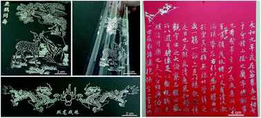
To investigate the printability of liquid metal on substrates with different surface roughness, five kinds of materials are introduced as the target substrates and they include silicone wafer, glass, PVC plastic film, polydimethylsiloxane (PDMS) and paper. The RMS roughness of these substrates measured by atomic force microscopy are respectively 1.05 nm, 1.09 nm, 3.81 nm, 22.6 nm and 202 nm, and the measured mean contact angles between Galinstan and them as shown in Fig. 3(A) are respectively 119.2°, 125.7°, 111.4°, 134.1° and 136.3°. Fig. 3(B) presents a circuit pattern printed on silicone wafer substrate. Though the roughness of the silicone wafer is a rather small value, the liquid metal ink can still be screen printed on its surface due to the driving air pressure from the airbrush. Fig. 3(C) and (D) present a painting pattern printed on PVC plastic film in flat and curling states, respectively. As PVC film has excellent flexibility, it can be used as the substrate to fabricate flexible printed circuit board (FPCB) with the liquid metal screen printing method. Fig. 3(E) shows a dragon playing with a pearl pattern printed on black paper substrate, while Fig. 3(F) depicts liquid metal calligraphy works printed on red paper substrate. As paper is one of the most available materials, it can be foreseen that paper-based liquid metal screen printing will have significant potentials in fabricating metal calligraphy & painting, as well as paper-based flexible electronics.
image file: c5ra10295b-f3.tif
Fig. 3 (A) The measured contact angles of Galinstan droplets on substrates with different surface roughnesses. The substrates are respectively silicone wafer, glass, PVC plastic film, PDMS and paper with roughnesses from small to large order. Error bars represent the standard deviation of the mean. (B) A circuit pattern printed on silicone wafer substrate. (C) A painting pattern printed on PVC plastic film substrate. (D) The printed painting pattern when the PVC substrate is curled. (E) Dragon playing with a pearl pattern printed on black paper substrate. (F) Liquid metal calligraphy works printed on red paper substrate. (G) Potted flower pattern printed on PDMS substrate. (H) RFID antenna pattern printed on glass substrate.

In addition, liquid metal ink can also be screen printed on the PDMS (as shown in Fig. 3(G)) and the glass substrates (as shown in Fig. 3(H)) which are respectively flexible and rigid substrate materials. It is worth mentioning that all the patterns presented in Fig. 3(B)–(H) are screen printed in 15 seconds to 3 minutes, indicating a rapid manufacturing process.

2.4. Stability of the printed line resistor

The electrical stability of the conductive line is essential for manufacturing circuits. And several typical experiments are performed to illustrate the reliability of the printed line with liquid metal screen printing method. The resistance–time relationship curve of a printed line resistor as shown in Fig. 4(A) is measured for 60 hours in indoor environment. It can be observed that overall the resistance of the line resistor is almost a constant value (fluctuates between 2.331 Ω and 2.340 Ω) at the room temperature (fluctuates between 26.730 °C and 27.436 °C). This stability property of the resistor is due to the surface oxide layer which prevents the liquid metal from flowing. To investigate the influence of repeated bending on the resistance of the liquid metal resistor, bending test is performed and the result is presented in Fig. 4(B). The resistance value is measured every 50 bending cycles with the bending radius R of 15 mm. It fluctuates slightly (between 2.022 Ω and 2.240 Ω) for all the 1000 cycles, which indicates that the printed line resistor possesses favorable mechanical stability. For each cycle, the resistor printed on the PVC plastic film is bended at −180°, −90°, 0°, 90° and 180°, respectively. As shown in the inset of Fig. 4(B), the measured resistance values present some discrepancy between each other which can be attributed to the tiny deformation of the liquid metal resistor, as well as the effect of contact resistance.
image file: c5ra10295b-f4.tif
Fig. 4 (A) The endurance test of the resistance of a printed line resistor on PVC plastic film substrate. Inset is the liquid metal line resistor whose size is 98 mm × 2 mm (length × width). (B) The resistance values of a liquid metal line resistor whose size is 95 mm × 2 mm (length × width) at different bending cycles. The inset are the resistance values of the line resistor at different bending angles, and the illustration of the bending angle α and the bending radius R. Error bars represent the standard deviation of the mean.

2.5. Characterization of a printed RFID tag

In order to evaluate the feasibility of manufacturing electronics with the liquid metal screen printing method, a RFID antenna tag is printed on PVC plastic film substrate as shown in Fig. 5(A). The measured frequency response of the reflection coefficient is presented in Fig. 5(B), along with the simulated values by Ansoft HFSS. The measured resonant frequency is 986.7 MHz, compared with the simulated result of 955.2 MHz. Factors including the measurement errors are responsible for the discrepancy between the measured and the simulated results. As the printed antenna tag is in liquid state at room temperature, they should be encapsulated with PDMS or silicone rubber to resist destroying. In addition to flexible electronics, fabricating of rigid electronics with high melting point metal inks via screen printing method is also of great practical significance and will be studied in the future.
image file: c5ra10295b-f5.tif
Fig. 5 (A) A RFID antenna tag screen printed on PVC plastic film. (B) Simulated and measured reflection coefficient of the printed antenna.

3. Conclusions

The liquid metal screen printing method introduced in this work demonstrated a rapid manufacturing technique for fabricating circuits or metal patterns. With such method, complex patterns could be printed within several seconds to several minutes on flexible or rigid substrates. The pattern shape was determined by the shape of the open areas of the screen which could transfer the liquid metal microdroplets. To improve the printing quality, the screen should be placed in tight contact with the substrate to weaken the influence of airflow which comes from the airbrush. Five kinds of materials including silicone wafer, glass, PVC, PDMS and paper with surface roughness ranging from 1.05 nm to 202 nm could all be utilized as the substrates to perform liquid metal screen printing. The printed line resistor on PVC substrate exhibited favorable reliability and mechanical stability which were verified by the endurance and bending tests. For practical illustration, a liquid metal RFID antenna tag was manufactured and the measured resonant frequency value was in good agreement with the simulated result. Further investigations include hybrid printing of multilayer devices such as transistors and paper LEDs with diverse kinds of inks. As a time and energy saving method, liquid metal screen printing possesses broad market prospect in manufacturing flexible electronics, metal tags and metal calligraphy & painting.

4. Experimental section

4.1. Preparation of the liquid metal ink

Three kinds of pure metals (Ga, In and Sn) with the purity above 99.99% (4N) were weighed according to the ratio of 68.5[thin space (1/6-em)]:[thin space (1/6-em)]21.5[thin space (1/6-em)]:[thin space (1/6-em)]10.0, and then they were added in a beaker which was heated in water bath at 85–90 °C. These pure metals were stirred continuously for about 40 min to achieve uniformity.

4.2. Characterization

The SEM and EDX images were obtained through a field emission scanning electron microscope (QUANTA FEG 250) to characterize the screen mesh, the width and thickness and the surface chemical composition of the printed liquid metal track. The 3D surface topography of the liquid metal pattern was obtained by using an optical profiler (NT9100M). The surface roughness of silicone wafer, glass, PVC, PDMS and paper were obtained through an atomic force microscope (Veeco Dimension D3100 AFM). The contact angles between the liquid metal and the five substrates were measured by using a contact angle meter (JC2000D3, Shanghai). The resistance of the printed line resistor was measured through a data acquisition unit (Agilent 34972A). The frequency response of the reflection coefficient of this antenna was measured with a network analyzer (Agilent N5230A).

4.3. Wiring and encapsulating devices

Cupric powder conductive was employed to connect the printed RFID antenna tag and the feeder line. The liquid metal antenna tag was encapsulated with a kind of neutral transparent single component RTV (room temperature vulcanizing) silicone rubber, which would be cured in air at room temperature after 24 hours later.

Acknowledgements

This work is partially supported by the Research Funding of the Chinese Academy of Sciences.

References

  1. D. A. Serban, P. Greco, S. Melinte, A. Vlad, C. A. Dutu, S. Zacchini, M. C. Lapalucci, F. Biscarini and M. Cavallini, Small, 2009, 5, 1117 CAS .
  2. E. Coronado, C. Marti-Gastaldo, J. R. Galan-Mascaros and M. Cavallini, J. Am. Chem. Soc., 2010, 132, 5456 CrossRef CAS PubMed .
  3. M. Cavallini, D. Gentili, P. Greco, F. Valle and F. Biscarini, Nat. Protoc., 2012, 7, 1668 CrossRef CAS PubMed .
  4. S. H. Jeong, A. Hagman, K. Hjort, M. Jobs, J. Sundqvist and Z. G. Wu, Lab Chip, 2012, 12, 4657 RSC .
  5. B. A. Gozen, A. Tabatabai, O. B. Ozdoganlar and C. Majidi, Adv. Mater., 2014, 26, 5211 CrossRef CAS PubMed .
  6. Y. J. Kim, S. Kim, J. Hwang and Y. J. Kim, J. Micromech. Microeng., 2013, 23, 065011 CrossRef .
  7. B. Perez-Lopez and A. Merkoci, Adv. Funct. Mater., 2011, 21, 255 CrossRef CAS PubMed .
  8. K. Nomura, H. Ushijima, R. Mitsui, S. Takahashi and S. Nakajima, Microelectron. Eng., 2014, 123, 58 CrossRef CAS PubMed .
  9. Y. Zheng, Z. Z. He, J. Yang and J. Liu, Sci. Rep., 2014, 4, 4588 Search PubMed .
  10. J. W. Boley, E. L. White, G. T. C. Chiu and R. K. Kramer, Adv. Funct. Mater., 2014, 24, 3501 CrossRef CAS PubMed .
  11. A. Tabatabai, A. Fassler, C. Usiak and C. Majidi, Langmuir, 2013, 29, 6194 CrossRef CAS PubMed .
  12. W. J. Hyun, E. B. Secor, M. C. Hersam, C. D. Frisbie and L. F. Francis, Adv. Mater., 2015, 27, 109 CrossRef CAS PubMed .
  13. J. L. Chang and J. M. Zen, Electrochem. Commun., 2006, 8, 571 CrossRef CAS PubMed .
  14. P. M. Hallam, D. K. Kampouris, R. O. Kadara and C. E. Banks, Analyst, 2010, 135, 1947 RSC .
  15. A. Martinez-Olmos, J. Fernandez-Salmeron, N. Lopez-Ruiz, A. R. Torres, L. F. Capitan-Vallvey and A. J. Palma, Anal. Chem., 2013, 85, 11098 CrossRef CAS PubMed .
  16. K. Ryu, A. Upadhyaya, V. Upadhyaya, A. Rohatgi and Y. W. Ok, Prog. Photovoltaics, 2015, 23, 119 CAS .
  17. E. Cabrera, S. Olibet, D. Rudolph, P. E. Vullum, R. Kopecek, D. Reinke, C. Herzog, D. Schwaderer and G. Schubert, Prog. Photovoltaics, 2015, 23, 367 CAS .
  18. J. P. Metters, E. P. Randviir and C. E. Banks, Analyst, 2014, 139, 5339 RSC .
  19. D. Janczak, M. Sloma, G. Wroblewski, A. Mlozniak and M. Jakubowska, Sensors, 2014, 14, 17304 CrossRef PubMed .
  20. A. B. Dighe, D. P. Dubal and R. Holze, Z. Anorg. Allg. Chem., 2014, 640, 2852 CrossRef CAS PubMed .
  21. M. Fekete, W. Riedel, A. F. Patti and L. Spiccia, Nanoscale, 2014, 6, 7585 RSC .
  22. S. Y. Chung, S. Kim, J. H. Lee, K. Kim, S. W. Kim, C. Y. Kang, S. J. Yoon and Y. S. Kim, Adv. Mater., 2012, 24, 6022 CrossRef CAS PubMed .
  23. K. S. Kim, K. H. Jung and S. B. Jung, Microelectron. Eng., 2014, 120, 216 CrossRef CAS PubMed .
  24. X. Cao, H. T. Chen, X. F. Gu, B. L. Liu, W. L. Wang, Y. Cao, F. Q. Wu and C. W. Zhu, ACS Nano, 2014, 8, 12769 CrossRef CAS PubMed .
  25. D. A. Pardo, G. E. Jabbour and N. Peyghambarian, Adv. Mater., 2000, 12, 1249 CrossRef CAS .
  26. E. Horvath, A. Torok, P. Ficzere, I. Zador and P. Racz, Acta Polytechnica Hungarica, 2014, 11, 29 Search PubMed .
  27. Q. Zhang, Y. X. Gao and J. Liu, Appl. Phys. A: Mater. Sci. Process., 2014, 116, 1091 CrossRef CAS PubMed .
  28. S. H. Jeong, K. Hjort and Z. G. Wu, Sensors, 2014, 14, 16311 CrossRef CAS PubMed .
  29. P. Surmann and H. Zeyat, Anal. Bioanal. Chem., 2005, 383, 1009 CrossRef CAS PubMed .
  30. F. Scharmann, G. Cherkashinin, V. Breternitz, G. Hartung, T. Weber and J. A. Schaefer, Surf. Interface Anal., 2004, 36, 981 CrossRef CAS PubMed .
  31. D. Kim, P. Thissen, G. Viner, D. W. Lee, W. Choi, Y. J. Chabal and J. B. Lee, ACS Appl. Mater. Interfaces, 2013, 5, 179 CAS .
  32. M. E. Schrader, Langmuir, 1995, 11, 3585 CrossRef CAS .

This journal is © The Royal Society of Chemistry 2015