
 Open Access Article
 This Open Access Article is licensed under a
 Creative Commons Attribution 3.0 Unported Licence
Correlating flat band and onset potentials for solar water splitting on model hematite photoanodes†
Beniamino
Iandolo‡
a,
Haixiang
Zhang
b,
Björn
Wickman
a,
Igor
Zorić
a,
Gavin
Conibeer
b and
Anders
Hellman
*a
aDepartment of Applied Physics, Chalmers University of Technology, SE-41296 Göteborg, Sweden. E-mail: anders.hellman@chalmers.se
bSchool of Photovoltaic and Renewable Energy Engineering, University of New South Wales, Sydney, NSW 2052, Australia
First published on 29th June 2015
Abstract
Hematite (α-Fe2O3) is a very promising material for solar water splitting that requires a high anodic potential to initiate the oxygen evolution reaction (OER). In this work, we explore the correlation between the downshift in flat band potential of hematite, Vfb, and in onset potential of OER, Vonset, caused by prolonged annealing. We observed a cathodic shift (i.e., towards lower potentials) of 200 mV of Vonset on model photoanodes consisting of ultra-thin hematite films, upon increasing the oxidation time during fabrication and without any further modifications. Detailed physical characterization, electrochemical impedance spectroscopy, and Mott–Schottky analysis revealed a quantitative correlation between the cathodic shift of Vonset and a lowering of Vfb. We identified a reduction in concentration of grain boundaries with increasing oxidation time, as the mechanism behind the observed shift of the Vfb. The approach presented here can be seen as a complementary strategy to co-catalysts and other post-fabrication treatments to lower Vonset. Moreover, it is generically applicable to photoelectrodes used to carry out oxidation and reduction half–cell reactions.
Introduction
Solar radiation is a sustainable energy source whose potential greatly exceeds the current global energy demand. However, as the Sun does not shine continuously everywhere on Earth, developing efficient and economically viable methods to concentrate and store the harvested radiation is required. An appealing possibility is to store solar energy in the form of chemical bonds, in a similar fashion to natural photosynthesis, via photoelectrochemical (PEC) water splitting.1,2 A key factor for a commercially successful introduction of PEC water splitting is the development of photoelectrodes that meet strict requirements in terms of efficiency, durability, and availability.3Among the 200+ compounds tested for water splitting after the seminal work by Fujishima and Honda,4–6 hematite (α-Fe2O3) has emerged as a promising candidate for the water oxidation half-cell reaction (or oxygen evolution reaction, OER).7,8 This is thanks to the following properties of hematite: (i) it has an optical bandgap energy, EG, between 1.9 and 2.2 eV (depending on the fabrication route), appropriate to absorb a wide range of solar photon energies; (ii) it is stable under operation in neutral and alkaline conditions;9 and (iii) its constituents are earth-abundant and non-toxic elements.10 Based on the value of EG alone, a maximum theoretical solar to chemical energy conversion efficiency of 16.8% has been predicted for hematite based water oxidation.11 However, the efficiency values achieved hitherto are at most of about 3%.12 This is mainly due to: (i) a low hole collection efficiency, particularly for energies close to the bandgap;13 and (ii) a slow OER at the hematite/electrolyte interface, hence, requiring highly anodic potentials to achieve a reasonable rate.14
The typical energetics of a junction between hematite and an aqueous electrolyte is illustrated schematically in Fig. S1a.† As the materials brought into contact reach equilibrium, electrons transfer from hematite to the electrolyte will cause an upward band bending of the conduction and valence bands in the semiconductor. By applying an external bias to the semiconductor, the extent of the band bending can be increased, decreased and even reversed to be downwards. By definition, the flat band potential, Vfb, is the electrochemical potential applied to the semiconductor that reduces this band bending to zero. Commonly found values of Vfb for hematite range between 0.4 and 0.8 V vs. the reversible hydrogen electrode (RHE).15–18 For any potential more anodic than Vfb, the upwards band bending drives photogenerated holes towards the solid/liquid interface. Then, if the quasi-Fermi energy level of the holes EF,p is lower than the OER potential, water oxidation can in principle take place. In practice, however, EF,p is higher than the top of the valence band due to a notably small value of photovoltage (Vph) sustained by hematite. Also, as mentioned above, the OER kinetics is slow. These two factors lead to the existence of a large (typically at least 400 mV) difference between Vfb and the experimentally observed Vonset. The quantity Vonset − Vfb is often referred to as overpotential for the OER.19
Fig. S1b† illustrates the present gap between the performance of state-of-the-art hematite photoanodes and those of an ideal hematite photoanode. The latter delivers a photocurrent density (per projected unit area, Apro) jmax of 12 mA cm−2 at an electrochemical potential equal to or lower than 0.8 V vs. RHE.20 The former photoanodes, instead, show an illuminated Vonset of about 1.15 V vs. RHE and reach 4 mA cm−2 at 1.54 V vs. RHE.21 Therefore, both enhancing jmax and shifting Vonset towards more cathodic potentials are needed to fully exploit the potential of hematite.
The issue of increasing jmax is typically addressed by material doping22–24 to increase conductivity and hence improve current collection, and/or nanostructuring to increase the surface to volume ratio.25–27 Most successful attempts to shift Vonset cathodically can be grouped into three categories:28,29 (i) introducing OER co-catalysts, to accelerate the OER kinetics;25,30,31 (ii) depositing under- or overlayers of other oxides, to create homo- or heterojunctions leading to reduced overpotential or to enhanced photovoltage;32–35 (iii) post-fabrication treating the hematite surface.36–38 The aforementioned modifications of hematite result into either an increase of the Vph, or into a decrease of the overpotential (i.e., Vonset − Vfb). A complementary approach to further shift Vonset cathodically is to lower Vfb. This will lead to a lowered Vonset provided that worsening of other properties in the system, for instance slower OER kinetics or smaller Vph, does not overshadow this beneficial effect. Such a strategy is rarely investigated owing to the established concept that Vfb is an intrinsic property of the semiconductor given a certain fabrication procedure. Nevertheless, combining this strategy to others of proven efficiency is likely to be required to meet the goal of 12 mA cm−2 at 0.8 V vs. RHE, especially considering that jmax is only achieved at a potential which is 0.3–0.4 V more anodic than Vonset.
A systematic investigation of the correlation between the modification of Vfb and that of the photoelectrochemical performance of hematite photoanodes is missing in the literature, to the best of our knowledge, and we aim at correcting such deficiency in this work. Also, we address the following questions: can we shift the OER Vonset on hematite by lowering Vfb without any further post-fabrication treatments, and without affecting negatively other PEC properties of the material? And if so, can we explain the observed trend(s) regarding Vfb and Vonset? Besides the intrinsic interest in deepening the understanding of hematite based water splitting, we anticipate that lowering Vfb of hematite, combined with strategies already established to shift Vonset cathodically (and to enhance jmax), will help reaching the ideal performance of hematite photoanodes.
In order to address these questions, we employed a model system consisting of flat hematite films, and studied the impact of varying a key fabrication parameter, namely the oxidation time, on the PEC performance of the photoanodes. Our fabrication route (dry thermal oxidation of iron thin films) yields hematite photoanodes showing typical jmax between 0.1 and 0.12 mA cm−2 (see results and discussion). This is commensurate with the jmax measured by other groups on flat hematite thin films in which the density of majority charge carriers is determined by oxygen vacancies in the lattice.16,18,24,39 We notice that these values of current per projected unit area Apro are more than an order of magnitude lower than those recorded on nanostructured, doped champion photoanodes. We mainly attribute such a difference to the fact that our samples are much flatter and therefore characterized by a smaller hematite/electrolyte contact area Acontact (for instance, the latter was determined to be 28 for nanocauliflower hematite fabricated by atmospheric pressure chemical vapor deposition25). Moreover, we stress that we focus here on Vonset and Vfb, rather than on jmax. Our samples are an excellent model system given the focus of this work, thanks to a less complicated interpretation of PEC data – in particular from electrochemical impedance spectroscopy, EIS – as compared to that obtained on nanostructured photoelectrodes.20 We present samples with a range of values of Vonset, where the lowest ones are commensurate with those measured on the best hematite photoanodes without post-fabrication treatments. We stress that it is important to analyze and understand the processes on all samples, with both high and low values of Vonset in order to make models that can be extrapolated beyond state-of-the-art.
By prolonging the oxidation time of the films, and without any further treatment, we demonstrated a cathodic shift of Vonset of about 200 mV. From EIS characterization, we obtained insights in the OER kinetics of the photoanodes and discriminated between losses taking places in the bulk of hematite and at the hematite/electrolyte interface. We used Mott–Schottky analysis to extract the Vfb in our films and thus compare the observed trends in Vonset and Vfb. Then, we employed a series of physical characterization techniques to investigate the physical mechanism(s) behind the observed PEC trends. We used scanning electron microscopy (SEM) and atomic force microscopy (AFM) to observe the morphology and topography of the hematite, respectively. We determined the oxidation state of Fe in the proximity of the hematite surface and investigated possible surface doping by means of X-ray photoemission spectroscopy (XPS). We measured the optical absorption coefficient and bandgap of hematite using optical spectroscopy. Finally, we used transmission electron microscopy (TEM) to qualitatively investigate the microstructure of hematite in terms of relative grain orientation and grain boundaries. We identified a reduction in concentration of grain boundaries upon increasing oxidation time as cause for the lowering of flat band potential.
Methods
Fabrication
Photoelectrodes were fabricated on indium tin oxide (ITO, PGO GmbH, sheet resistance ≤ 20 Ω per square) or fluorine doped tin oxide (FTO, Solaronix, sheet resistance ≤ 10 Ω per square) covered glass substrates, according to a procedure described in detail elsewhere.40 Briefly, iron films were deposited on top of the respective substrate by physical vapor deposition (PVD 225, Kurt. J. Lesker, base pressure < 5 × 10⁻⁷ mbar). Complete conversion into Fe2O3 was achieved with thermal oxidation at 350 °C in a mixed N2![[thin space (1/6-em)]](https://www.rsc.org/images/entities/char_2009.gif) :O2 (3:1) atmosphere. The temperature was ramped from room temperature up to 350 °C at a rate of 15 °C min−1, after which the temperature was kept constant at 350 °C for a time tox, which was between 0 and 24 h depending on the sample. Then, the furnace was allowed to cool down to room temperature naturally.
:O2 (3:1) atmosphere. The temperature was ramped from room temperature up to 350 °C at a rate of 15 °C min−1, after which the temperature was kept constant at 350 °C for a time tox, which was between 0 and 24 h depending on the sample. Then, the furnace was allowed to cool down to room temperature naturally.
Characterization
SEM of the as-prepared samples was performed in a Zeiss Supra 60 VP microscope, using an acceleration voltage of 5 kV. The topography was investigated with a Bruker Dimension ICON AFM. Five 500 × 500 nm scans were acquired in tapping mode for each sample, and the roughness for each scan was calculated after image flattening using NanoScope Analysis v1.40r1 software (Bruker). The thickness of the films was measured with a Dektak 150 surface profiler (Veeco). The optical absorption in the films deposited on ITO was measured with a Cary 5000 spectrophotometer (Varian) equipped with the External Diffuse Reflectance Accessory (DRA) 2500, which accounts for optical reflection. The absorption in hematite was determined by using a blank ITO substrate as reference. The latter was exposed to the same furnace treatment as the hematite covered substrates. The absorption coefficient α was extracted from the measured absorption assuming a Lambertian absorption profile. The values obtained were used for Tauc analysis according to the formula (αhν)0.5 = (hν − EG), where hν is the photon energy, EG is the bandgap energy of the semiconductor and the exponent 0.5 indicates an indirect (i.e., phonon assisted) transition. The values of EG for different samples were obtained by extrapolating to the horizontal axis the linear part of the curves in the Tauc plots in the energy range between 2.1 and 2.3 eV. XPS spectra were acquired in a Perkin Elmer Phi 5500 setup (base pressure < 10−10 mbar) using AlKα radiation of 1.4866 keV. The XPS spectra were shifted using the C(1s) peak corresponding to adventitious carbon (284.5 eV) as a reference. TEM was performed with a field emission Jeol JEM 2100F microscope at 200 kV. To facilitate the TEM analysis, thin silicon nitride membranes (‘TEM windows’41) were used as support and hematite films were fabricated on the membranes using the same procedure as described above.Photoelectrochemical measurements
All PEC characterization of the ITO/hematite samples was carried out in a Teflon based cell (Accent PN4300), using an Autolab PGSTAT302N potentiostat. A three electrodes configuration was used, with the ITO/hematite as working electrode, a Pt wire as counter-electrode and a Ag/AgCl (KCl saturated) reference electrode. A 0.1 M KOH solution (pH = 12.9) was used as the electrolyte, and the working electrode was illuminated from the front in all measurements. The Ag/AgCl electrode potential, VAg/AgCl, was converted to the reversible hydrogen electrode, VRHE, using the equation VRHE = VAg/AgCl + V0Ag/AgCl + 0.059 × pH, where V0Ag/AgCl = 0.197 V at 25 °C. The light source was a 300 W Xe lamp (Cermax_LX_300) equipped with a UV filter (420 nm cut-off wavelength, Schott), positioned at a distance of 38.5 cm from the PEC cell. At such a distance, the total light intensity impinging on the working electrode was estimated from product specification to be about the same as AM 1.5 filtered illumination provided by a solar simulator (100 mW cm−2), although with a different spectral distribution. Cyclic voltammetry was performed between 0.76 and 1.76 V vs. RHE at a scan rate of 10 mV s−1. To obtain the photocurrent density j, the current was divided by the projected area in contact with the electrolyte, Apro. Only the forward scan from cathodic to anodic potentials was plotted for ease of visualization. For the EIS measurements, the DC voltage was changed in steps of 0.1 V from 1.76 to 0.86 V vs. RHE, on top of which an AC voltage of root mean square amplitude of 10 mV and frequency varying between 105 and 0.1 Hz was superimposed. Nyquist plots obtained under illumination were fitted using the software Nova v. 1.9 (Metrohm Autolab). Mott–Schottky analysis was performed in the dark, in the same potential window, using an AC voltage with a frequency of 104 Hz. Cyclic voltammetry of the FTO/hematite samples was performed in the same 3-electrode configuration, using a Gamry ref. 600 potentiostat, in a H-type glass cell with working electrode and counter-electrode compartments separated by a glass frit. The working electrode compartment had flat optical windows to allow for the illumination of the samples. A solar simulator (SKU SS150, Sciencetech. Inc.) was the illumination source, with intensity at the working electrode surface adjusted to 100 mW cm−2 using a NIST calibrated photodiode.Results and Discussion
In light assisted OER from water splitting, as explained above, two quantities are of key interest, namely the onset potential Vonset and the plateau photocurrent jmax measured before purely electrochemical water splitting is observed. Fig. 1 shows the results of the cyclic voltammetry measurements performed on samples with different tox under illumination and in the dark. While samples with tox between 0 and 12 h show a maximum photocurrent between 0.11 and 0.12 mA cm−2, those with longer tox show negligible photoactivity. This is most likely due to the loss of electrical conductivity of ITO when exposed at temperatures of 350 °C for prolonged times.42 Therefore, in the remainder of the manuscript we will focus on samples with tox ≤ 12 h.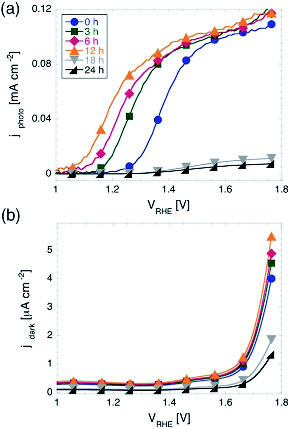 | ||
| Fig. 1 Current density j as function of electrochemical potential V for hematite films on ITO. (a) Photocurrent density under UV-filtered illumination from a Xe-lamp. The onset potential for the OER Vonset shifts of 200 mV towards more cathodic potentials for tox increasing from 0 to 12 h. For longer tox, the films show negligible photoactivity. (b) Current density measured in the dark. The onset potential shifts only by around 30 mV between tox = 0 h and tox = 12 h. | ||
The maximum photocurrent jmax does not depend significantly on tox for potentials more anodic than 1.6 V vs. RHE. As discussed in the introduction, the values jmax measured here are more than an order of magnitude lower than those measured on state-of-the-art photoanodes, however commensurate to those observed on photoanodes fabricated using similar routes.39 It is worth mentioning that we found an increase of jmax of about 20% as compared to hematite films fabricated via the same procedure and characterized in previous work.43 This difference is most likely caused by the differences in the spectral distribution of the illumination source. We recall that here the light intensity impinging on the sample was 100 mW cm−2, but not with an AM 1.5 spectral distribution.
Although all samples shown in Fig. 1a reach very similar values of jmax for high anodic potentials, they show a striking difference in Vonset, which moves towards more cathodic potentials for increasing tox. Considering the quantitative determination of Vonset, different definitions can be found in the literature. For example, Vonset has been defined as: (i) the potential at which the photocurrent exceeds a certain defined value,30 (ii) the potential at which dJ/dV exceeds a certain defined value,44 or (iii) the potential at which the tangent to the J(V) curve in the region of maximum slope intersects the J(V) curve measured in the dark.33 It should be noted that all these definitions are somewhat arbitrary and may be more or less appropriate depending on the shape of the J(V) curves at hand. For instance, using method (iii) can result in a situation where a curve with a steep slope will have a more anodic Vonset than one with a flatter slope, although they may have the same Vonset according to methods (i) and/or (ii). We note that the J(V) curves presented here show a very similar slope after the photocurrent starts rising. Therefore, although the choice of method to define Vonset might slightly affect the exact values extracted from the J(V) curves, the shifts in Vonset with varying tox will be practically be independent of the chosen method. Here we used method (i), with 10 μA cm−2 as a threshold in photocurrent density (corresponding to about 10% of jmax). According to this definition, we found Vonset to be equal to 1.28 V vs. RHE for tox = 0. Upon increasing tox from to 3, 6, and 12 hours, Vonset shifts significantly towards more cathodic potentials, to 1.19, 1.13, and 1.08 V vs. RHE, respectively.
The onset potential showed a much weaker dependency on tox for cyclic voltammetry in the dark, as shown in Fig. 1b. Using method (i) again (with threshold current corresponding to 10% of the maximum current observed in the dark in the potential window investigated), we found that the onset potential shifts only 30 mV in total when increasing tox from 0 to 12 h. This indicates that the effect of prolonging tox on the OER in the dark is negligible.
We further investigated the PEC properties of the photoanodes via EIS. Recent studies have established EIS as a powerful technique to characterize the dynamics of charge transfer at the hematite/electrolyte interface, as well as of charge transport in the bulk of the semiconductor.14,45 Data from EIS measurements is often shown in form of Nyquist plots, where the real component and negative imaginary component of the complex impedance Z are plotted on the horizontal and vertical axis, respectively. Fig. 2a shows the Nyquist plots obtained for the 6 h sample, under illumination, at some relevant values of DC bias. A qualitative decrease in total impedance is visible with increasing potential (at 1.16 V vs. RHE the impedance values at lower frequencies are well outside the range of impedance in the plot). The presence of two semicircles indicates that two time constants are present in the system. We found the same evolution of the Nyquist plots for increasingly anodic potential for all samples measured.
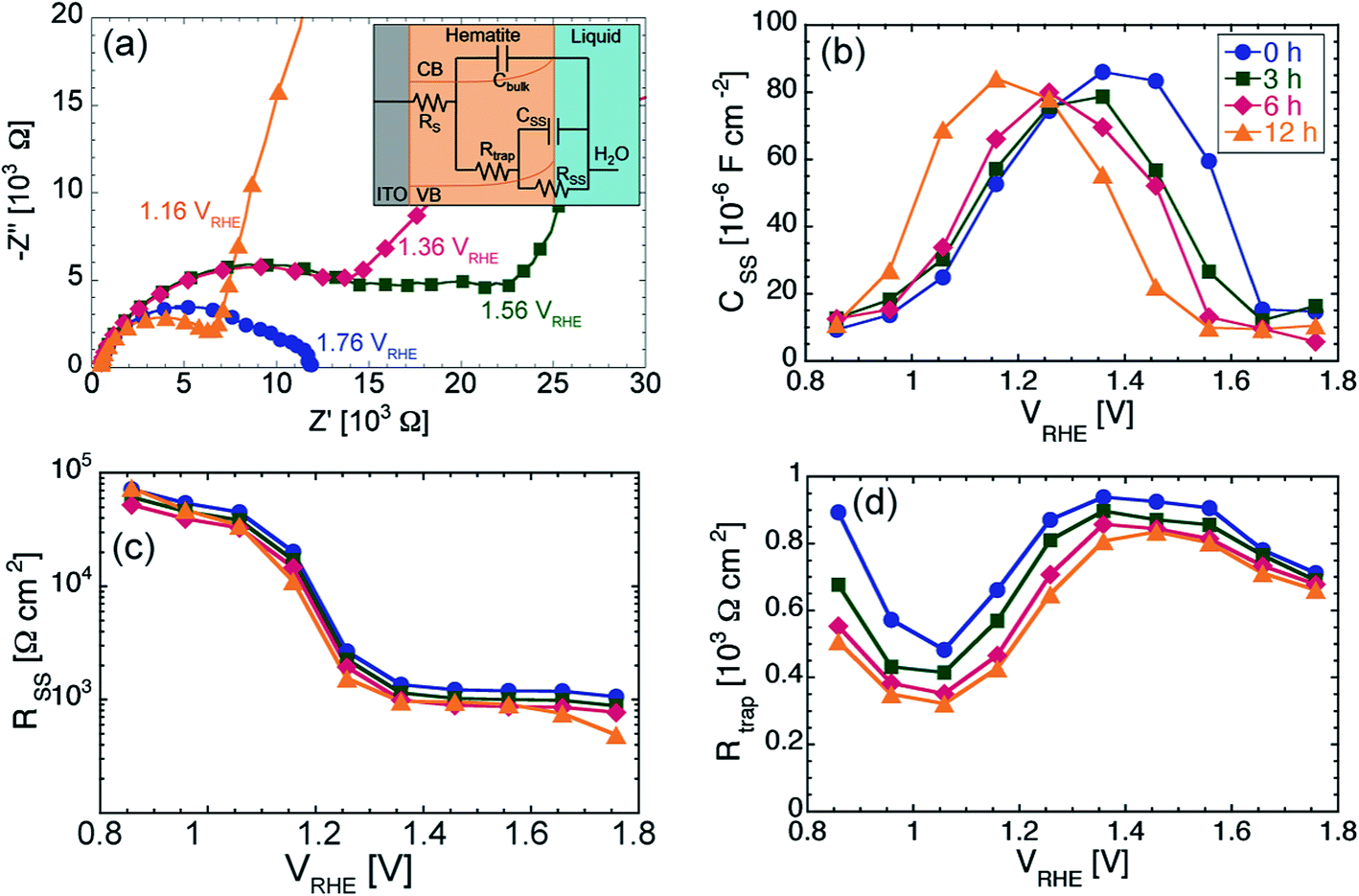 | ||
| Fig. 2 (a) Representative Nyquist plots obtained from EIS measurements on the tox = 6 h sample under illumination at different applied potential. Inset: equivalent circuit used to fit the Nyquist plots under illumination. (b–d) Results from the equivalent circuit fitting of the Nyquist plots. The following quantities are plotted as function of applied potential: (b) Surface states capacitance CSS, (c) Charge transfer resistance RSS, (d) trapping resistance Rtrap. | ||
In order to correlate changes in the Nyquist plots with changes in the properties of charge transport through the photoanode and of charge transfer at the hematite/semiconductor interface, equivalent circuit modeling is required. For photoelectrodes where water oxidation performance is hampered by slow OER kinetics, an appropriate circuit is shown in the inset of Fig. 2a, which has been discussed and employed previously for studying hematite photoanodes.8,45 In brief, the electrical components of this equivalent circuit are: RS, the contact resistance between ITO and hematite; Cbulk, the capacitance originating from the charge in the space-charge layer in hematite; Rtrap, the resistance associated with transport of charge through the bulk of hematite; CSS, the chemical capacitance associated with surface states at the hematite/electrolyte interface,46 and RSS, the resistance associated with charge transfer from hematite to the electrolyte. Within this model, the high and low frequency semicircles in the Nyquist plots are associated with bulk and surface properties of the photoanode, respectively. It is clear that the impedance associated with the low frequency semicircle decrease considerably with increasing potential, while the impedance associated with high frequency is basically independent of the applied bias.
By fitting of the Nyquist plots using the equivalent circuit described above, we extracted the values of CSS, Rtrap and RSS for all samples as function of the applied DC potential. The results are shown in Fig. 2b–d. For each sample, CSS(V) first increases for more anodic potential, reaches a maximum and then decreases back to about its initial value for the most anodic potentials. Moreover, the potential at which CSS(V) peaks is close to the onset potential Vonset. This fact is a signature that the OER under illumination takes place via surface states for potential values close to Vonset. These surface states are first charged and then discharged when the potential is sufficiently anodic to start the OER. We estimated the charge density on the surface state QSS by integrating CSS with respect to V. We found QSS to be between 38.2 and 39.2 μC cm−2 for the 12 h and 0 h samples, respectively. In other words QSS is basically constant regardless of tox. These observations, together with the weak dependency of the dark electrolysis onset potential on tox, point to very similar OER kinetics for all samples.
The hematite/electrolyte charge transfer resistance, RSS(V), is plotted in Fig. 2c, from which we see that the transfer of holes from the semiconductor to the electrolyte is not significantly affected by changing tox. Fig. 2d shows that the resistance associated with recombination of charge carriers in the bulk of the hematite, Rtrap(V), has a similar behavior for all samples, with a minimum at 1.06 V vs. RHE and a flatter region for potentials more anodic than 1.36 V vs. RHE. However, the values of Rtrap are clearly decreasing for increasing tox, with the strongest effect for potentials more cathodic than 1.56 V vs. RHE.
We can summarize the main findings of our equivalent circuit analysis as follows: (1) the results from the analysis of the CSS(V) and RSS(V) plots are additional evidence that varying tox does not affect the OER kinetics under illumination; (2) the decrease of Rtrap(V) with increasing tox for low anodic bias indicates a possible beneficial effect of prolonged oxidation time on the charge carrier transport within the films.
Mott–Schottky (MS) analysis is commonly performed in the dark, in order to extract not only Vfb, but also the donor/acceptor (for n- and p-type semiconductor, respectively) concentration, ND. For a perfectly planar semiconductor–electrolyte interface (i.e. where Apro = Acontact), the MS equation reads (Apro/Cbulk)2 = 2(V − Vfb − kbT/e)/(ε0εrND), where, Cbulk is the capacitance of the space-charge layer, kb is the Boltzmann constant, T is the absolute temperature, e is the elementary charge, ε0 is the permittivity of vacuum and εr is the relative permittivity of the semiconductor.47 The validity of this simple relationship between Cbulk and V − Vfb lies on the following assumptions: (i) Cbulk is much smaller than the capacitance CH associated with the Helmholtz layer in the electrolyte; (ii) the donors/acceptors are uniformly distributed in space, have all the same energy, and are all ionized; (iii) the width of the space-charge layer WSC is much smaller than the thickness d of the semiconductor. Under these assumptions, the MS plot is linear, and ND can be obtained from the relationship ND = 2/ε0εreS, where S is the slope of the plot, while Vfb is obtained from the intercept with the horizontal axis.
The MS plots for the values of tox investigated in this work are indeed linear for potentials between 0.86 and 1.36 V vs. RHE, as shown in Fig. 3a, while for potentials more anodic they show a concave shape. The latter could in principle be explained by assuming a special non-uniform distribution of ionized donors.48 In particular, one would have to assume a continuously increasing ND with increasing distance from the hematite/electrolyte interface. However, we do not consider such a possibility as plausible, since the oxidation of Fe into Fe2O3 is carried out for a sufficiently long time (including ramp up and cool down time) for the resulting films to have uniform electronic properties throughout their thickness.
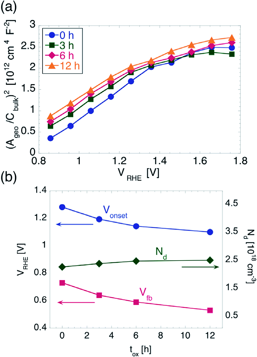 | ||
| Fig. 3 (a) Mott–Schottky plots for hematite films on ITO. (b) Onset potential Vonset and flat band potential in hematite Vfb (left y-axis) and donor concentration ND (right y-axis) as function of tox. | ||
Instead, the considerably small thickness of our hematite films makes the approximation WSC ≪ d questionable. It has been shown that, in photoanodes consisting of a thin TiO2 deposited on ITO, the depletion region can extend into the ITO for sufficiently high anodic potentials, and the MS equation needs to be modified to take this effect into account.49 In particular, the MS plot was predicted to have two distinct slopes, one at more cathodic potentials, which is determined by the εr and ND of the TiO2, and one for more anodic potentials, which is determined by the εr and ND of the ITO. The potential Vth where the slope changes is the potential at which WSC in the TiO2 equals the TiO2 thickness. The following relationship between d and Vth was then found: d = ε0εrS0.5(Vth − V kT/e)0.5. We followed a similar approach to further analyze our MS plots. We note that the potentials applied here were not so anodic that the second slope could be determined without a large deviation. Therefore we used, for the slope at high anodic potentials, the values of εr (ITO) = 9 and ND (ITO) = 1020 cm−3, which are normally found for ITO films with similar sheet resistance as compared to the ones used here.49,50 Once Vth is determined and d is known, εr can be extracted. We found that εr only varies between 18.9 and 19 when increasing tox. We note that these values for εr are considerably smaller than the values of 32 and 80 often plugged into the simplest form of the MS equation to directly extract ND.28,51 Within the approach used here, instead, we can use the εr extracted from our MS plots to obtain ND. We found the latter to increase from 2.28 × 1018 cm−3 to 2.52 × 1018 cm−3 with tox increasing from 0 to 12 h. From the measurements performed here we cannot determine unambiguously the origin of such difference in ND. Nevertheless, we stress that the increase of ND is only of a factor of 1.1, which we judge insufficient to explain the considerable Vonset shift found from cyclic voltammetry. Moreover, we found a quantitative correlation between the shift of Vonset and that of Vfb, as explained below.
In order to evaluate Vfb, we fitted the linear part of the MS plots, where only the properties of hematite come into play. Since we did not measure directly Acontact, we used the value of Apro (0.1 cm2) as contact area for all samples, and we found Vfb to shift from 0.73 V to 0.53 V vs. RHE. Such a shift towards more negative potentials follows closely the shift of Vonset observed during the cyclic voltammetry measurements, as illustrated in Fig. 3b. The difference between Vonset and Vfb is about 550 mV irrespective of tox, which points once again to very similar OER kinetics for all samples. This is in contrast to the reduction in Vonset obtained upon employing electrocatalysts or other surface coatings, which do not change Vfb appreciably.30,52 The shift of Vfb could in principle be caused by a decrease in the Helmholtz layer capacitance. A treatment of the solid/liquid interface that includes explicitly CH has shown to predict a MS plot with the same slope as in the simplest case,53 but with an intercept shifted by an amount equal to ε0εreND/2CH2 = 1/S CH2. In order to obtain the extracted 200 mV shift of Vfb, one would have to assume an increase of CH of a factor of 25 upon increasing tox from 0 to 12 h, which we judge unreasonable given the similarity of the hematite/electrolyte interface properties as extracted by EIS under illumination.
Another possible mechanism of the observed shift of Vfb could be the introduction of In or Sn atoms from ITO into the hematite, which would be consistent with the slight increase of ND extracted previously. The modification of Vfb upon doping has been observed, for instance, in other semiconductors used in PEC cells/solar cells.54,55 However, direct evidence that neither In nor Sn did not diffuse from ITO to the surface of the photoanodes is offered by XPS measurements, as discussed further on. Furthermore, we performed control cyclic voltammetry measurements on hematite samples deposited FTO, which is known to be thermally stable up to 700 °C. The photocurrent measurements carried out on the FTO based films demonstrated a similar cathodic shift of the onset potential upon increasing tox from 3 to 12 h to that obtained for the films deposited on ITO, which confirms that the observed Vonset is also independent of the electron collection layer underneath hematite.
Thanks to the MS analysis, we established a quantitative correlation between the extracted shift of Vfb and the shift of Vonset observed during the cyclic voltammetry measurements. While Vfb is typically determined by the properties of the solid/liquid junction and of the space-charge layer, Vonset is determined by the properties of the whole photoelectrode. However, due to the very small thickness of the films used here, it is reasonable to consider both Vfb and Vonset as determined by the properties of the whole film. Nevertheless, it is not clear at this stage if the shift of Vfb is correlated to any change in the physical properties of the hematite films, which we characterized in deeper detail.
We measured the hematite thickness by surface profiler, and found it to be 25 ± 2 nm irrespective of tox. SEM inspection did not indicate an obvious difference in morphology between the samples, as shown in Fig. S2.† Investigation by AFM led to the conclusion that the topography of the samples is not affected appreciably by prolonging tox, as shown in Fig. S3.† The root mean square roughness, Rq, was found to vary only very slightly from 2.3 ± 0.15 nm for tox = 0 h to 2.32 ± 0.18 nm for tox = 12 h, which justifies the use of the same value of contact area for all the samples.
We carried out XPS measurements on sample with tox equal to 0 and 12, in order to perform analysis of chemical composition and electronic states of the surface of the films, and the results are summarized in Fig. 4. First, we notice that no peaks appear in the survey scans (panel a) at energies corresponding to peaks indicating the presence of In or Sn, which is a further, direct confirmation that neither In nor Sn did not diffuse up to the hematite surface. Second, the normalized XPS Fe(2p) and O(1s) signals (panels b and c respectively) are practically identical in shape, indicating that surface composition of the sample and oxidation state of the iron within a few nm from the surface are not affected by changing tox.
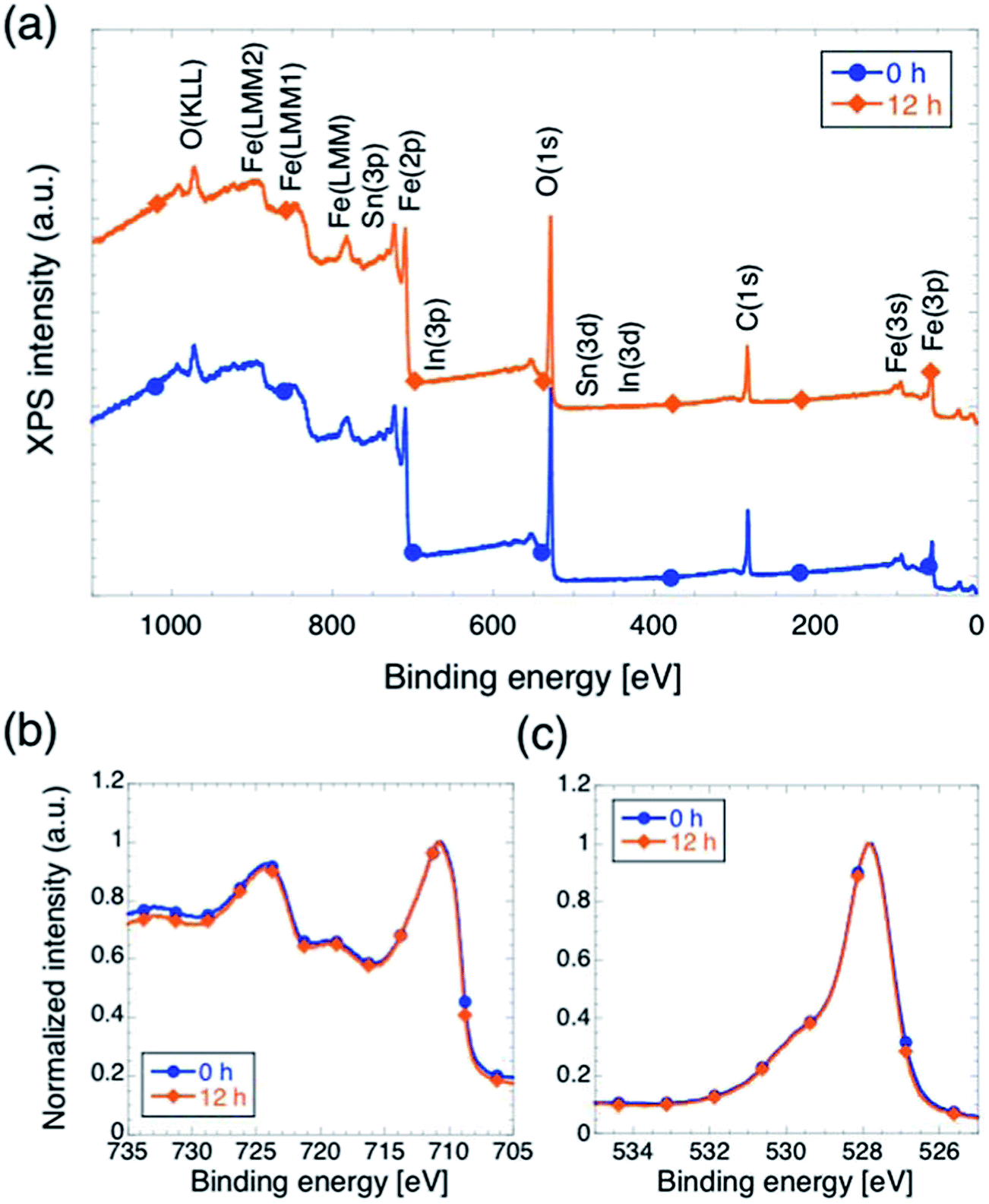 | ||
| Fig. 4 XPS characterization for hematite films on ITO with tox = 0 h and tox = 12 h. (a) Survey scans with peaks identification. The curves are shifted on the vertical axis for ease of visualization. Clearly, no In or Sn is detected. (b). Normalized intensity profiles of Fe(2p) peaks. (c) Normalized intensity profiles of O(1s) peaks. | ||
We characterized the optical properties of the films using spectrophotometry, and the results are summarized in Fig. 5. It is worth mentioning that the use of the integrating sphere accessory to perform these measurements enabled us to directly measure the sum of scattered (including reflected) light and transmitted light, from which we obtained the absorption Abs = 1 − (Sca + Tr). The onset of optical absorption between 630 and 600 nm indicates that the oxidation process is complete even for tox = 0 h, i.e. when ramping up the temperature to 350 °C and starting the cool-down immediately afterwards. The absorption profile of the 0 h sample, however, differs slightly from the other spectra. In particular, the absorption is lower for wavelengths between 420 and 560 nm, whereas it is slightly higher between 560 and 640 nm. Inspection of the Tauc plots in Fig. 5b reveals that EG increases from 1.9 to 1.98 eV upon increasing tox from 0 to 3 hours, while further increasing tox leaves EG unmodified. We believe, however, that the observed discrepancy in optical absorption between the 0 h samples and the other samples cannot account for the observed difference in Vonset, for the following reasons. First, an increase in number of absorbed photons (with no other changes in the electrochemical properties of the film) should lead to an increased jmax rather than a shift in Vonset.15 Second, the optical absorption is not affected by further increasing tox from 3 hours to 6 or 12 hours, although Vonset is shifted further cathodically. On the other hand, the slightly lower value of jmax measured on the 0 h sample as compared to the other samples (for which jmax is the same within a 5% margin) can be attributed to the lower optical absorption between 420 and 560 nm observed for the 0 h sample.
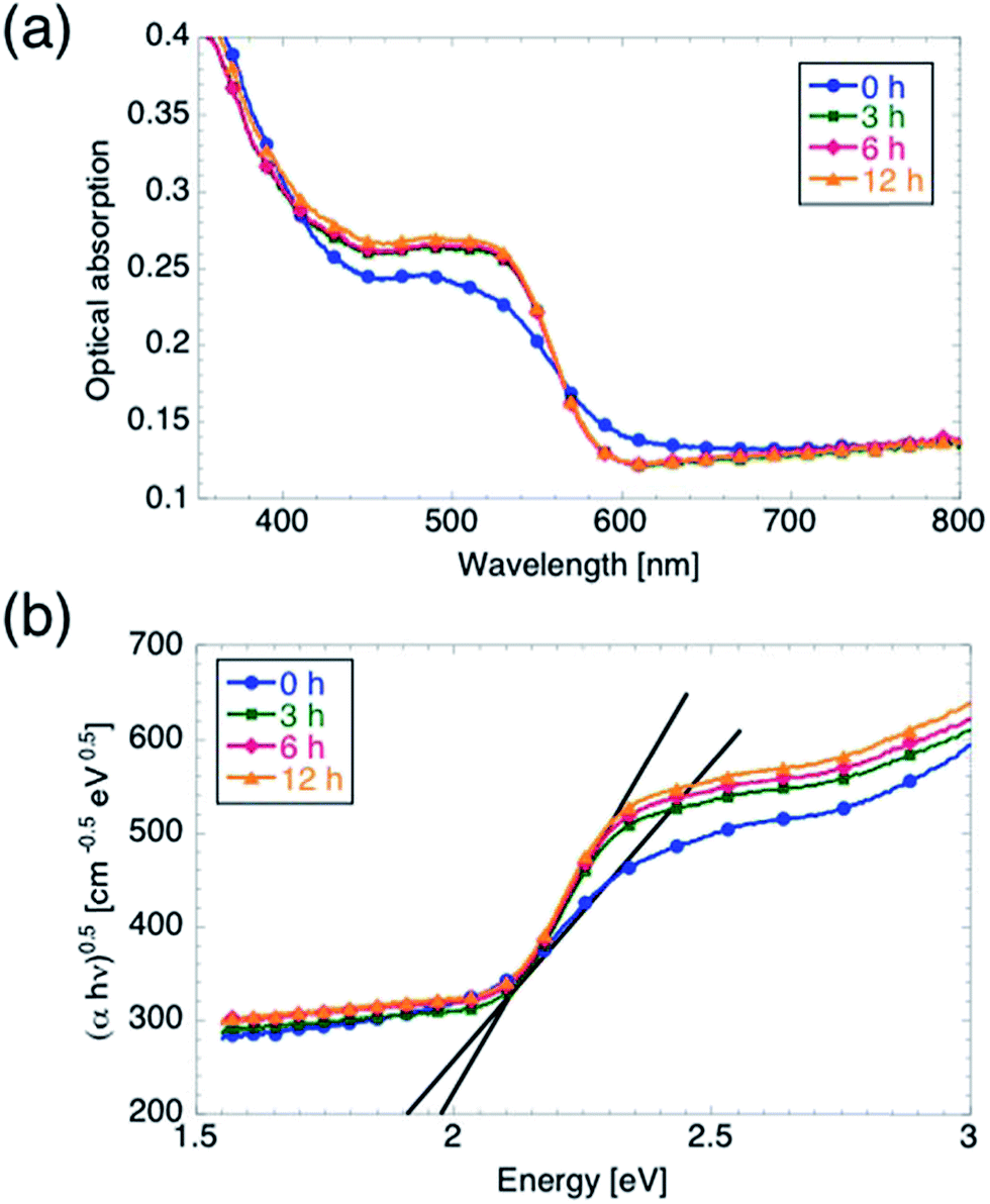 | ||
| Fig. 5 Optical characterization of hematite films. (a) Optical absorption as function of wavelength. (b) Bandgap energy determination from Tauc analysis performed assuming an indirect bandgap in hematite. The bandgap energy EG increases from 1.90 to 1.98 eV between the 0 h sample and the other samples. | ||
Complete conversion of Fe into hematite was confirmed in a previous work56 by XRD measurements performed on samples at least 4 times thicker than those used here. It is thus reasonable to assume than the same holds for the ultra-thin films employed in this study. In spite of several attempts, we did not manage to obtain significant XRD data on these 25 nm thick films. Therefore, we resorted to TEM characterization in order to investigate the properties of the films in terms of crystallinity and grain boundaries. The results are summarized in Fig. 6. While all the films are polycrystalline as expected, we did observe clear changes in the sample at the nanoscale. In particular, the crystallite size increases distinctly with increasing tox. For the lowest tox, the average crystallite size is of the order of 10 nm or smaller. Since the film thickness is 25 nm there are several crystallites in the TEM field of view, which makes it somewhat difficult to interpret the images and in particular to perform quantitative analysis of the crystallite size distribution. Nonetheless, it is qualitatively clear that the crystallites grow with increasing tox. For example, panel (d) (tox = 12 h) shows crystallites that are significantly larger in size than the film thickness (several tens of nm).
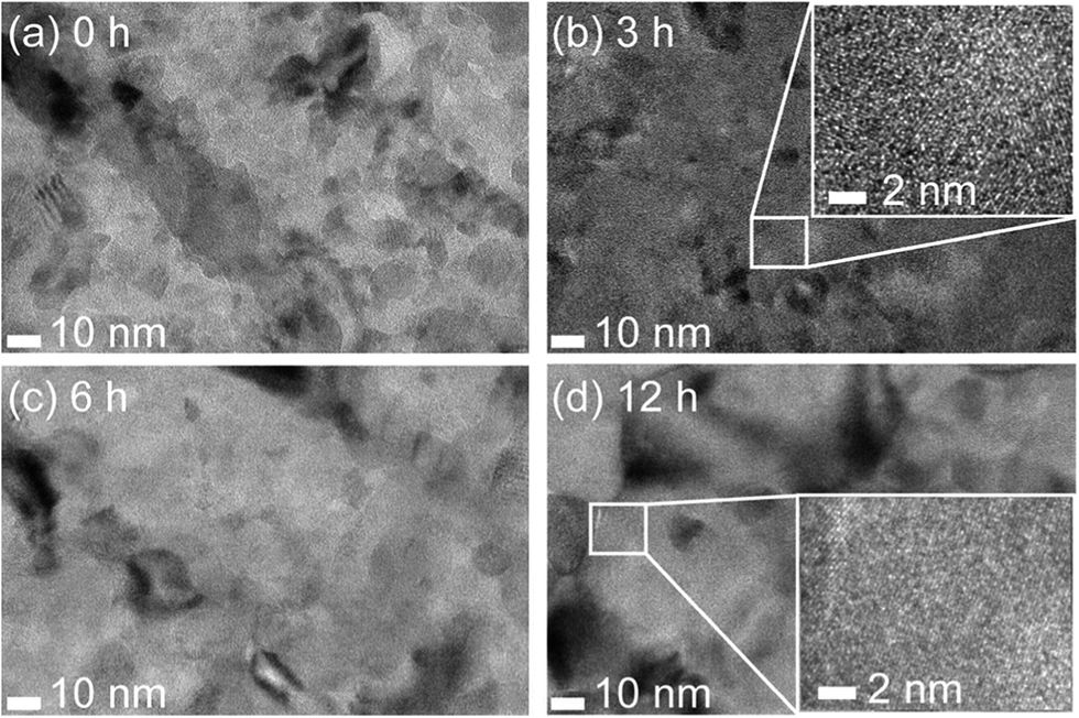 | ||
| Fig. 6 TEM images of hematite films with tox = 0 h (a), 3 h (b), 6 h (c) and 12 h (d). Panels (b) and (d) also include insets showing high resolution images. | ||
In view of the information obtained from the TEM analysis, we propose the following qualitative explanation for the shift of Vfb, and therefore of Vonset. The increase of grain size for increasing tox determines a decrease in density of grain boundaries in hematite. These grain boundaries are typically associated with potential drops that reduce the efficiency of charge transport within the film.21 Therefore, by reducing the density of grain boundaries we also reduce the extent of the potential drops that are detrimental for the charge transport within hematite. In other words, a stronger band bending in hematite is obtained by increasing tox. As a consequence, a larger potential is needed in order to reach the condition of zero band bending in hematite, which is Vfb by definition. Therefore, Vfb shifts towards lower, or towards more cathodic potentials. We observe that such mechanism is consistent with all data extracted from the EIS measurements, in particular with the decrease in bulk trapping resistance Rtrap recorded under illumination. Moreover, we highlight that the proposed mechanism for the shift of Vfb, and thus of Vonset, is consistent with the similar values of jmax measured at highly anodic applied potentials. In this regime, in fact, the mechanism limiting the photocurrent in hematite photoanodes is the number of photons absorbed, rather than the charge transport within the film or the OER kinetics at the surface.15
Conclusions
In conclusion, in this work we systematically studied the correlation between the OER Vonset and Vfb of hematite based photoelectrodes. We addressed the question if the OER onset potential Vonset on hematite can be lowered by lowering the flat band potential Vfb of the material, and if this can be achieved without post-fabrication treatments. To this end, we employed a model system based on hematite ultra-thin films, and we determined how Vonset and Vfb are affected by the oxidation time during fabrication of the photoanodes. We demonstrated a cathodic shift of Vonset of 200 mV on increasing tox from 0 to 12 hours, without any further surface treatment. A combination of AFM, XPS characterization and EIS measurements under illumination indicated that increasing tox did not affect the electrochemical properties of the hematite/electrolyte interface. EIS also pointed to increased charge transport efficiency within hematite for prolonged tox. Mott–Schottky analysis revealed a quantitative correlation between the cathodic shift of Vonset and a shift of Vfb in the same direction. The fact that the difference between Vonset and Vfb is independent of tox offered further confirmation that varying the oxidation time did not affect the kinetics of the OER. From TEM analysis we proposed that the mechanism responsible for the shift of Vfb hematite, and therefore for the shift of the OER Vonset, is the improved quality of the films in terms of increased grain size and thus of reduced density of grain boundaries, leading to an increase in band bending in the semiconductor. The results presented here point at the possibility of enhancing the performance of hematite in terms of lowering Vonset by improving the intrinsic properties of the semiconductor, which we expect to be compatible with further strategies towards the same goal such as introduction of underlayers, addition of electrocatalysts, or other surface coatings and post-fabrication treatments. Furthermore, the concepts presented in the Introduction regarding the energetics of a semiconductor/electrolyte interface can be applied not only to hematite, but much more generically to both n-type and p-type semiconductors. Therefore, the approach of shifting Vfb can readily be applied to any semiconductor-based photoelectrodes, i.e. not only lowering Vfb for n-type semiconductors used in oxidation half-cell reactions, but also increasing Vfb for p-type semiconductors employed for reduction half-cell reactions.Acknowledgements
BI, BW, and IZ thank Formas (project numbers 219-2011-959 and 229-2009-772) for financial support. AH acknowledges support from the Swedish Research Council. BI thanks the Areas of Advance for Material Science and for Nanotechnology at Chalmers University of Technology supporting his external research stay at UNSW. Dr. Yunhau Ng and Prof. Rose Amal from the School of Chemical Engineering (UNSW) are gratefully acknowledged for providing the potentiostat for the PEC measurements performed at UNSW. GC and HZ acknowledge support from the Australian Government through the Australian Renewable Energy Agency (ARENA). The Australian Government, through ARENA, is supporting Australian research and development in solar photovoltaic and solar thermal technologies to help solar power become cost competitive with other energy sources. The views expressed herein are not necessarily the views of the Australian Government, and the Australian Government does not accept responsibility for any information or advice contained herein.References
- M. Grätzel, Nature, 2001, 414, 338–344 CrossRef PubMed.
- Y. Tachibana, L. Vayssieres and J. R. Durrant, Nat. Photonics, 2012, 6, 511–518 CrossRef CAS.
- T. Bak, J. Nowotny, M. Rekas and C. C. Sorrell, Int. J. Hydrogen Energy, 2010, 27, 991–1022 CrossRef.
- A. Fujishima and K. Honda, Nature, 1972, 238, 37–38 CrossRef CAS PubMed.
- M. D. Hernández-Alonso, F. Fresno, S. Suárez and J. M. Coronado, Energy Environ. Sci., 2009, 2, 1231 Search PubMed.
- F. E. Osterloh, Chem. Mater., 2008, 20, 35–54 CrossRef CAS.
- Z. Li, W. Luo, M. Zhang, J. Feng and Z. Zou, Energy Environ. Sci., 2013, 6, 347 CAS.
- B. Iandolo and A. Hellman, Angew. Chem., Int. Ed. Engl., 2014, 53, 13404–13408 CrossRef CAS PubMed.
- L. R. Yeh and N. Hackerman, J. Electrochem. Soc., 1977, 124, 833 CrossRef CAS.
- P. C. K. Vesborg and T. F. Jaramillo, RSC Adv., 2012, 2, 7933 RSC.
- A. Murphy, P. Barnes, L. Randeniya, I. Plumb, I. Grey, M. Horne and J. Glasscock, Int. J. Hydrogen Energy, 2006, 31, 1999–2017 CrossRef CAS.
- J. Brillet, J. Yum, M. Cornuz, T. Hisatomi, R. Solarska, J. Augustynski, M. Graetzel and K. Sivula, Nat. Photonics, 2012, 6, 824–828 CrossRef CAS.
- L. A. Marusak, R. Messier and W. B. White, J. Phys. Chem. Solids, 1980, 41, 981–984 CrossRef CAS.
- L. M. Peter, J. Solid State Electrochem., 2012, 17, 315–326 CrossRef.
- H. Dotan, K. Sivula, M. Grätzel, A. Rothschild and S. C. Warren, Energy Environ. Sci., 2011, 4, 958 CAS.
- A. P. Singh, A. Mettenbörger, P. Golus and S. Mathur, Int. J. Hydrogen Energy, 2012, 37, 13983–13988 CrossRef CAS.
- G. Rahman and O.-S. Joo, Int. J. Hydrogen Energy, 2012, 37, 13989–13997 CrossRef CAS.
- R. Franking, L. Li, M. A. Lukowski, F. Meng, Y. Tan, R. J. Hamers and S. Jin, Energy Environ. Sci., 2013, 6, 500 CAS.
- M. Barroso, S. R. Pendlebury, A. J. Cowan and J. R. Durrant, Chem. Sci., 2013, 4, 2724 RSC.
- Photoelectrochemical Hydrogen Production, ed. R. van de Krol and M. Grätzel, Springer US, Boston, MA, 2012, vol. 102 Search PubMed.
- S. C. Warren, K. Voïtchovsky, H. Dotan, C. M. Leroy, M. Cornuz, F. Stellacci, C. Hébert, A. Rothschild and M. Grätzel, Nat. Mater., 2013, 12, 842–849 CrossRef CAS PubMed.
- I. Cesar, K. Sivula and A. Kay, J. Phys. Chem. C, 2008, 772–782 Search PubMed.
- A. Kleiman-Shwarsctein, Y.-S. Hu, A. J. Forman, G. D. Stucky and E. W. McFarland, J. Phys. Chem. C, 2008, 112, 15900–15907 CAS.
- S. Kumari, A. P. Singh, D. Deva, R. Shrivastav, S. Dass and V. R. Satsangi, Int. J. Hydrogen Energy, 2010, 35, 3985–3990 CrossRef CAS.
- A. Kay, I. Cesar and M. Graetzel, J. Am. Chem. Soc., 2006, 15714–15721 CrossRef CAS PubMed.
- Y. Lin, S. Zhou, S. W. Sheehan and D. Wang, J. Am. Chem. Soc., 2011, 133, 2398–2401 CrossRef CAS PubMed.
- A. Mao, G. Y. Han and J. H. Park, J. Mater. Chem., 2010, 20, 2247 RSC.
- K. Sivula, F. Le Formal and M. Grätzel, ChemSusChem, 2011, 4, 432–449 CrossRef CAS PubMed.
- M. J. Katz, S. C. Riha, N. C. Jeong, A. B. F. Martinson, O. K. Farha and J. T. Hupp, Coord. Chem. Rev., 2012, 256, 2521–2529 CrossRef CAS.
- L. Badia-Bou, E. Mas-Marza, P. Rodenas, E. M. Barea, F. Fabregat-Santiago, S. Gimenez, E. Peris and J. Bisquert, J. Phys. Chem. C, 2013, 117, 3826–3833 CAS.
- S. D. Tilley, M. Cornuz, K. Sivula and M. Grätzel, Angew. Chem., 2010, 122, 6549–6552 CrossRef.
- F. Le Formal, K. Sivula and M. Grätzel, J. Phys. Chem. C, 2012, 116, 26707–26720 CAS.
- F. Le Formal, N. Tétreault, M. Cornuz, T. Moehl, M. Grätzel and K. Sivula, Chem. Sci., 2011, 2, 737 RSC.
- T. Hisatomi, F. Le Formal, M. Cornuz, J. Brillet, N. Tétreault, K. Sivula and M. Grätzel, Energy Environ. Sci., 2011, 4, 2512 CAS.
- T. Hisatomi, H. Dotan, M. Stefik, K. Sivula, A. Rothschild, M. Grätzel and N. Mathews, Adv. Mater., 2012, 24, 2699–2702 CrossRef CAS PubMed.
- Y.-S. Hu, A. Kleiman-Shwarsctein, G. D. Stucky and E. W. McFarland, Chem. Commun., 2009, 2652–2654 RSC.
- M. Zhang, W. Luo, N. Zhang, Z. Li, T. Yu and Z. Zou, Electrochem. Commun., 2012, 23, 41–43 CrossRef CAS.
- D. Cao, W. Luo, J. Feng, X. Zhao, Z. Li and Z. Zou, Energy Environ. Sci., 2014, 7, 752–759 CAS.
- P. Hiralal, S. Saremi-Yarahmadi, B. C. Bayer, H. Wang, S. Hofmann, K. G. Upul Wijayantha and G. A. J. Amaratunga, Sol. Energy Mater. Sol. Cells, 2011, 95, 1819–1825 CrossRef CAS.
- B. Iandolo, T. J. Antosiewicz, A. Hellman and I. Zorić, Phys. Chem. Chem. Phys., 2013, 15, 4947–4954 RSC.
- A. W. Grant, Q.-H. Hu and B. Kasemo, Nanotechnology, 2004, 15, 1175–1181 CrossRef CAS.
- R. Synowicki, Thin Solid Films, 1998, 313–314, 394–397 CrossRef CAS.
- B. Iandolo, B. Wickman, B. Seger, I. Chorkendorff, I. Zorić and A. Hellman, Phys. Chem. Chem. Phys., 2014, 16, 1271–1275 RSC.
- F. Le Formal, M. Grätzel and K. Sivula, Adv. Funct. Mater., 2010, 20, 1099–1107 CrossRef CAS.
- B. Klahr, S. Gimenez, F. Fabregat-Santiago, T. Hamann and J. Bisquert, J. Am. Chem. Soc., 2012, 134, 4294–4302 CrossRef CAS.
- J. Bisquert, Phys. Chem. Chem. Phys., 2008, 10, 49–72 RSC.
- Z. Chen, H. N. Dinh and E. Miller, Photoelectrochemical Water Splitting, Springer, New York, NY, 2013 Search PubMed.
- J. Schoonman, J. Electrochem. Soc., 1981, 128, 1154 CrossRef CAS.
- R. van de Krol, J. Electrochem. Soc., 1997, 144, 1723 CrossRef CAS.
- J. E. A. M. van den Meerakker, E. A. Meulenkamp and M. Scholten, J. Appl. Phys., 1993, 74, 3282 CrossRef CAS.
- J. A. Glasscock, P. R. F. Barnes, I. C. Plumb and N. Savvides, J. Phys. Chem. C, 2007, 111, 16477–16488 CAS.
- B. Klahr, S. Gimenez, F. Fabregat-Santiago, J. Bisquert and T. W. Hamann, J. Am. Chem. Soc., 2012, 134, 16693–16700 CrossRef CAS PubMed.
- M. Tomkiewicz, J. Electrochem. Soc., 1979, 126, 1505 CrossRef CAS.
- M. Radecka, K. Zakrzewska, M. Wierzbicka, A. Gorzkowska and S. Komornicki, Solid State Ionics, 2003, 157, 379–386 CrossRef CAS.
- R. Beranek and H. Kisch, Electrochem. Commun., 2007, 9, 761–766 CrossRef CAS.
- B. Iandolo and M. Zäch, Aust. J. Chem., 2012, 65, 633 CrossRef CAS.
Footnotes |
| † Electronic supplementary information (ESI) available. See DOI: 10.1039/c5ra10215d |
| ‡ Current address: Center for Electron Nanoscopy, Technical University of Denmark, DK-2800 Kgs. Lyngby, Denmark. |
| This journal is © The Royal Society of Chemistry 2015 |