Qiong Nianab,
Martin Y. Zhangab,
Dong Linab,
Suprem Dasa,
Yung C. Shinc and
Gary J. Cheng*abc
aBirck Nanotechnology Center, Purdue University, West Lafayette, IN 47906, USA. E-mail: gjcheng@purdue.edu
bSchool of Industrial Engineering, Purdue University, West Lafayette, IN 47906, USA
cSchool of Mechanical Engineering, Purdue University, West Lafayette, IN 47906, USA
First published on 19th June 2015
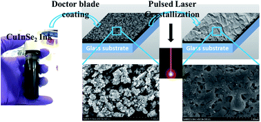
Direct pulsed laser crystallization (DPLC) of large area printed nanoparticle-inks is investigated to form a crystalline copper indium diselenide (CIS) thin film. This technique has great potential to be utilized in scalable device production due to its atmospheric processing and high yield rate. It is found that CIS nanoparticles of 20 nm-diameter can grow to micro scale large crystals in a film after DPLC. The internal imperfections including grain boundary, inter crystal gaps and voids were reduced significantly. The effects of laser intensity and pulse number on the deposited thin film are investigated. The localized field enhancement around nanoparticle contacts is believed to be responsible for nanoparticle welding and crystal growth near the CIS film surface area during DPLC. The complete crystallization of CIS nanoparticles along the depth direction is attributed to thermal diffusion driven rapid melting/solidification. Moreover, it was found that the microstructure change in the CIS film after DPLC influences the optical and electrical performance significantly. A typical increase of 7.9% (visible range) and 19.2% (near infrared range) in the optical absorbance is obtained under optimal DPLC conditions and a band-gap shrinkage (ΔEg) of the CIS thin film after DPLC leads to broader acceptance of solar spectrum of 100 nm. The results from the Raman spectrum and photoluminescence (PL) of the thin films under various laser conditions reveal that the improvement of the optoelectronic properties of the CIS thin film is related to the reduction of the crystal defect level in the thin film.
In order to reduce the internal imperfections, various post crystallization techniques after low cost fabrication are developed to densify the film structure and increase grain size. Among them, rapid thermal annealing (RTA)3 has been widely investigated, as well as direct pulsed laser crystallization (DPLC),8,9 for efficient and effective crystallization. However, RTA is expensive to be scaled up in industry due to some intrinsic issues such as temperature required, quasi-static temperature change leading to poor control of grain size and use of costly vacuum/inert gas systems. In addition, RTA is a non-selective heating process, not suitable for cutting-edge low melting point and large area substrates. DPLC has several advantages such as: (1) processing speed and large area processing: DPLC process make use of direct nanosecond-pulse laser interaction with target nanocrystals. If equipped with beam scanner (>10 m s−1) and commercial available diode pump solid state (DPSS) laser with frequency of 50–100 kHz, DPLC provides a fast speed, low cost, large area processing technique; (2) selective processing: different materials absorb laser energy at different wavelengths, such as CIS at visible region, while transparent conductive layer (i.e. aluminum-doped ZnO) absorbs laser at ultraviolet region. By selecting appropriate laser wavelength, DPLC only selectively processes the target and keeps other materials intact, which might be able to boost cutting edge organic based devices10–12 and solution based coatings.13–15 Exploring ultra-fast laser beam with small heat effective zone for selective crystallization, this process is efficient, in micro second scale, as demonstrated in our prior works.16,17
In this study, the mechanism of laser nanoparticle interaction is systemically investigated in order to find out the effects of laser processing conditions on the crystallinity of the thin film. During DPLC, the contacts between nanoparticles are localized heated and jointed to form a large crystal. With number of pulse increases, the crystal size gets bigger and bigger due to reduction of surface energy in nanoparticles, grain boundaries, inter-crystal gaps and inter-nanoparticle voids, as schematically illustrated in Fig. 1a. Field emission scanning electron microscopy (FESEM) characterization in Fig. 1b shows clear comparison before/after DPLC under optimal processing conditions. The microstructures after DPLC will be analyzed to show their effects on optical and electrical properties of thin film.
After crystallization process, FESEM is utilized to observe the morphological features of the CIS thin film after DPLC. Both top surface and cross sectional morphology are characterized. Focused ion beam contrast channeling (FIBCC) technique is used to confirm the growth of CIS crystals by determining the grain size. Lambda 950 visible-near infrared (NIR) spectrophotometer is used to measure the transmittance and absorbance spectra of CIS, and accordingly band gap is determined by plotting the absorbance squared versus energy, and followed by extrapolation to zero. Properly calibrated D8 Focus X-ray diffraction (XRD) facility (Bruker) is utilized to determine the maintained structural property of CIS processed by DPLC. Raman spectra are characterized by Confocal Raman microscope equipped with a motorized sample stage. Spectra Pro-300i is used to measure photoluminescence of DPLC processed CIS thin film.
During DPLC, two processing parameters played important roles: laser intensity and pulse number. To investigate the optimal processing condition for CIS nanoparticles (diameter = 20–40 nm), a series of experiments were carried out. Fig. 2 shows the effect of laser intensity on CIS film microstructure with fixed pulse number. For pulse number subject to 30, different laser intensities irradiated at the CIS thin film led to completely different surface morphology. When laser intensity was relatively low (2 MW cm−2), very few crystals grow occurred, as shown in Fig. 2a. This was attributed to inadequate thermal energy causing insufficient crystal growth or crystal melting. When laser pulse with a higher intensity (3.2–3.8 MW cm−2) was applied, obvious growth occurs to most of crystals but still leave several discrete nanoparticles, as shown in Fig. 2b and c. When 4.8 MW cm−2 was applied, crystal growth occurs to almost all crystals. The contact between nanoparticles was modified, resulting in good homogeneity and surface smoothness in Fig. 2d. Thus, it was considered that 4.8 MW cm−2 as the optimal intensity for current series of samples. However, higher laser intensity like 5.4 and 6.7 MW cm−2 would damage the film quality because of excess thermal energy in DPLC, for instance, the film would end up with either poor porous structure (Fig. 2e) or ablation at the surface (Fig. 2f). Neither of these two cases is favorable for CIS film practical application. The laser intensity effect mainly attributes to the peak temperature increase, where higher intensity brings more energy delivery which increases the peak temperature. If the peak temperature is too high, the CIS film would be vaporized or even ablated, resulting in poor film quality.
The effect of pulse number was characterized as presented in Fig. 3, under fixed laser intensity of 4.8 MW cm−2. Cross-section images in Fig. 3 show that crystal growth occurs not only on top surface, but also along thickness direction. As compared between Fig. 3a and b, in the first several pulses, oxygenic ligand and dispersant brought in synthesis and coating were removed, leading to close-packed and densified film structure. This initial laser pulses delivery eliminates the nanoparticles agglomeration, decreases the inter-particle gaps and benefits following crystallization. With more laser pulses coming in (10–20 pulse), the crystallization starts penetrating deeper to around 500 nm thick. Crystallization also could be demonstrated by the nanoparticles merging and large crystal forming, which is shown in Fig. 3c and surface morphology insert. Along with multi-pulse delivery continues, such as 20–25 pulses applied, the crystallization thickness extends to almost through the whole film in Fig. 3d. The crystallization penetrates deeper due to heat transfer along thickness, since gaps between nanoparticles are reduced by the first several pulses therefore heat diffuses more easily and CIS film with bigger grains in top layer possesses higher thermal and electrical conductivities than CIS film with small grains.18 With more laser pulses coming in, the more grown crystals on top conduct thermal energy at a faster rate within the thin film thereby boost the crystallization process (both population and depth). Finally, after 30 pulses, the crystal growth propagated through the entire thin film to form large crystals as seen in Fig. 3e and surface morphology insert. Comparing Fig. 3a–e, it clearly shows a great reduction of inner imperfections, such as gaps, voids and grain boundaries. The growth of crystals and decrease of inter-crystal gaps are confirmed by FIBCC technique.19,20 In Fig. 3a, the as-received CIS film has a loose structure with nanocrystals size in 20–40 nm. As the first few laser pulses coming in, top surface small grains with different orientations were observed at 100 nm scale. However, random holes are still obvious which indicates that crystallization is incomplete, though obvious grain growth. After 30 laser pulses, the whole region of interests (ROIs with approximately length × thickness = 4 × 2 μm) showed homogeneity, neither holes nor inter-crystal gaps was observed in Fig. 3f. IN addition, there is coherent boundary with the Mo layer underneath. This indicates the CIS nanocrystals grew up by merging with neighbor nanocrystals, thus inter-crystal gaps and void defects were overcome and large CIS crystals were formed.
To understand the interaction between CIS nanoparticles and pulse laser during DPLC, Comsol simulation was performed as shown in Fig. 4a with essential science indicators presented in Table 1.16,21,22 The laser pulse was modelled with a Gaussian electromagnetic wave as incident on a stack of nanoparticles. Gaussian beam laser was delivered with an electrical field of 1 V m−1. Each nanoparticle was modelled as having a circular cross-section in diameter of 20 nm with essential physical parameters input. The simulation provided local electric field strength distribution in the stacked nanoparticles shown in Fig. 4a, quantified by color legends. Local electrical field varied area to area, and concentrated as high as 14 V m−1 near contacts between nanoparticles due to surface plasmon polarization.23,24 It is well deserved to note that mainly nanoparticles contacts are able to enhance the local electrical field and form ‘hot spots’, while leaving particles themselves in low strength field. To further explore the heating process generated by the ‘hot spots’, the heat generation distribution from area to area was plotted in Fig. 4b contours. The heat generation was determined from the illumination power density multiplies the nanostructures absorption coefficient,25 that is, the power loss density calculated by Comsol Multiphysics®. As illustrated in Fig. 4b, the power loss density concentrates near particle contacts, and decrease as distance to contact increasing. The highest power loss density at nanoparticle contacts reaches ∼9.25 W m−3, while inside nanoparticles only generate as low as ∼1.05 W m−3. It implies that the localized heating of the contacted region between nanoparticle/nanoparticle, and nanoparticles/large crystals is one of the reason for welding nanoparticles together during DPLC, boost crystal growth to form large ones and moreover reduce internal imperfections in CIS film like voids and gaps.26,27
Laser parameters | CIS properties | |||||
---|---|---|---|---|---|---|
Wavelength (nm) | Pulse width (ns) | Repetition rate | Low frequency dielectric constant | High frequency dielectric constant | Density (g cm−3) | Carrier concentration density (cm−3) |
248 | 25 | 10 | 8.1 | 13.6 | 5.77 | 1.68 × 10¹⁸ |
These observations verified the mechanism of DPLC, which is in agreement with prior statements.8,9 During laser heating, photon energy is directly transferred to the electrons within a few picoseconds (ps), and resulted in heat leading to the melting of laser penetration depth region. Some other processes are considered in the heating: (1) laser intensity may be concentrated near nanoparticle contacts, because of surface plasmon polarization; (2) laser with photon energy greater than the band gap of CIS may generate electron–hole pairs which may absorb laser energy and be excited to a higher excited state; (3) the laser photon can cause inter-band and intra-band transitions which lead to the formation of dense and hot electron–hole solid state plasma. The heat would then be transferred into the sample, however with some delay due to heat diffusion. The heat diffused from surface through micrometers depth usually within 100 ns.8,9,28 The cooling occurred after the finish of laser pulse and heat propagation. Usually the cooling rate is proportional to the temperature gradient with a value up to 109 K s−1 at the surface and 108 K s−1 at 1 μm deep.9 Heat diffusion, controlled by material properties (such as thermal conductivity, thermal diffusivity, and specific heat) governs the localized temperature raising and cooling. Heat diffusion governing equation can be written as:29
![]() | (1) |
To investigate the effect of film microstructure modification on CIS optical property, the absorbance spectra of as-received and DPLC-processed CIS-based absorber layer were measured by Lambda 950 spectrophotometer in the wavelength range 400–1200 nm, as shown in Fig. 5a. DPLC-processed samples show obvious increase in absorbance throughout the visible to near infrared region (500–1200 nm), while less than 500 nm, a decrease in the absorbance is observed. In the range of 500 to 800 nm, optical absorbance has an average increase of 7.85% after DPLC treatment. It is worthy to point out that at the wavelength of 535 nm, there is a 5.2% increase in absorbance after DPLC treatment, this agrees with earlier reports.18,33–35 In the NIR (800 to 1200 nm) region as shown in Fig. 5b, the DPLC-processed sample is at least 19.2% (average) higher absorbance than the as-received sample (i.e. 11.6% at 800 nm, 18.4% at 1000 nm, and 29.3% at 1200 nm). This implies that potentially DPLC might improve the external quantum efficiency of the CIS-based solar cells as it absorbs more solar radiation. The absorbance enhancement attributes to film microstructure modification such as densified film, uniform and homogeneous surface and reduced internal imperfections. Since the stoichiometry of CIS has been well maintained and no indication of thermal decomposition was found after DPLC processing, according to typical XRD spectrum shown in Fig. 5a insert. The major diffraction peaks observed at 26.65°, 44.22°, 52.39°, 64.36°(2-Theta) can be indexed to the (112), (204)/(220), (116)/(312), (008)/(400) of the tetragonal crystal structure,3,4 respectively.
Band gap (Eg), a crucial factor determining material optical absorption, could be approximated by plotting the absorbance squared versus energy, and then extrapolating to zero.3 The band gap of as-received and DPLC-processed is determined to be 1.07 eV, and 1.01 eV, respectively, shown in Fig. 5c. Both two measured values are in good agreement with the reported value of bulk α-CIS (1.04 eV).3 However, a small band gap shrinkage (ΔEg = 60 meV) is observed after DPLC treatment, which widens the acceptable range of solar spectrum by 6% (extends from 1159 to 1228 nm). The absorbance increase and the band gap shrinkage suggest that DPLC-processed CIS thin films accept more solar irradiation compared with as-received films. The change of band gap and optical absorbance was observed by prior experimental and theoretical work reported in literature.36 It is found that band gap shrinkage strongly depends on the carrier concentration density (n). The relation between band gap shrinkage and carrier concentration is proposed by Burstein37 and Moss38 with B–M model which states that the band gap shrinkage (ΔEg) changes with the carrier concentration in the conduction band, as stated in eqn (2).39
![]() | (2) |
In order to understand the mechanism of DPLC, a systematic study was conducted to determine the optimal laser condition. The approach could be also applied to other nanoparticles to form crystallization thin films. The typical Raman spectra of CIS thin films processed by DPLC with different laser intensities and pulse numbers were collected and shown in Fig. 6. As observed, A1 peak located at 175 cm−1, which is normally observed in I–II–VI2 chalcopyrite compounds.39,41 The weak peaks located at 129 cm−1 and 213 cm−1 are corresponding to the single phase chalcopyrite structure CIS.42 The peak located at the highest wave number position 261 cm−1 is originated from the secondary phase such as copper selenite.43 According to,41,44 the appearance and intensity of A1 peak is strongly dependent on crystallinity of CIS thin film including crystal size, orientation and crystalline ordering; on the other hand, the presence of the secondary phase peak indicates highly disordered crystalline. In Fig. 7a, comparing with as-received sample, A1 peak of DPLC processed CIS films become stronger and secondary phase peak became weaker with higher laser intensity. This reflects a better film crystallinity and a trend to growth of the large mono-crystalline grains. However too high laser intensity like 6.7 MW cm−2 will ablate CIS thin film to generate worse film crystal quality, whose A1 peak became weaker and secondary phase peak become stronger. Fig. 6b–d show pulse number effect of laser intensities of 3.8 MW cm−2, 4.8 MW cm−2 and 5.4 MW cm−2, respectively. For two lower laser intensities 3.8 MW cm−2 and 4.8 MW cm−2, 50 and 30 pulses are required to get good film crystallinity. On the other hand, for laser intensity of 5.4 MW cm−2, 5 pulses is enough to supply thermal energy for recrystallization, while more pulses will introduce negative effect. Comparing the spectrum together in same scale, we can find 4.8 MW cm−2, 30 pulses the optimal condition for DPLC processed CIS film. Comparing Raman spectra of CIS processed by 3.8 MW cm−2 to as-received sample in Fig. 6a, a slight 2 cm−1 A1 peak shift away from 175 cm−1 was observed, which is also an indication of growth material referring to Zaretskaya etc.41
The crystallinity changes are concomitant with an improvement of the optoelectronic properties of the CIS thin film. Thus, typical room temperature photoluminescence (PL) could also be used to determine optimal condition. Fig. 7a presents the spectra of the 2 μm thick CIS thin films processed by DPLC with different laser intensities and 30 pulses. As shown in this figure, the peak of the as-received CIS thin film locates around 1200 nm, meaning the band gap is approximately 1.04 eV.3,45 However, the peaks of the recrystallized CIS thin films shift small amount to longer wavelength (lower energy) with increasing laser intensity. This is an indication of small band gap shrinkage of DPLC processed CIS thin film. This shrinkage is originated from carrier concentration drop after DPLC,37,38,40 which agrees well with absorbance spectra and Hall effect analysis in Table 2. On the other hand, according to,46 PL peak intensity strongly depends on surface carrier recombination process, relating with CIS thin film crystallinity and inter-grain defects level. With better film crystallinity and lower inter-grain defects density, it is easier for separated carriers diffusing to film surface for recombination, which will increase PL peak intensity.
Process | Resistivity (Ω cm) | Hall mobility (cm2 v−1 s−1) | Carrier concentration density (cm−3) |
---|---|---|---|
Before DPLC | 15.162 ± 0.026 | 0.266 ± 0.091 | (1.681 ± 0.599) × 1018 |
After DPLC | 0.182 ± 0.002 | 22.003 ± 3.920 | (1.493 ± 0.256) × 1018 |
Comparing with as-received sample, the DPLC processed CIS thin films show stronger PL peak with increasing laser intensity in Fig. 7a. We find 4.8 MW cm−2, 30 pulses is optimal condition to obtain strongest PL peak implying most improved CIS film. With too high laser intensity, such as 5.4 MW cm−2, a weak PL peak is observed. The decreasing PL peak intensity majorly attributes to import non-radiative recombination and rather poor film crystallinity.47 This poor film crystallinity results from that the excess thermal energy will ablate thin film.48
Fig. 7b–d present pulse number effect affected by laser intensity. For laser intensity of 4.8 MW cm−2, 30 pulses is optimal for DPLC presented in Fig. 7c. Too many pulses will ablate thin film and then degrade film crystal quality, bringing weaker PL peak. However, for lower laser intensity like 3.8 MW cm−2 shown in Fig. 7b, larger pulse number like 50 are needed to supply enough thermal energy for DPLC. Fig. 7d shows 4.8 MW cm−2, 30 pulses is the optimal condition for DPLC processed CIS film, which can mostly improve film crystallinity and lower inter-grain defects density to obtain strongest PL peak. This is in a good agreement with Raman spectra analysis.
This journal is © The Royal Society of Chemistry 2015 |