
 Open Access Article
 This Open Access Article is licensed under a
 Creative Commons Attribution 3.0 Unported Licence
Growth of nanocrystalline thin films of metal sulfides [CdS, ZnS, CuS and PbS] at the water–oil interface
P. John
Thomas
*a,
Gemma L.
Stansfield
b,
Nathanael
Komba
b,
David J. H.
Cant
b,
Karthik
Ramasamy
b,
Enteisar
Albrasi
b,
Hanan
Al-Chaghouri
b,
Karen L.
Syres
c,
Paul
O'Brien
bd,
Wendy R.
Flavell
e,
Egid
Mubofu
f,
Federica
Bondino
g and
Elena
Magnano
g
aSchool of Chemistry, Bangor University, Bangor, Gwynedd LL572UW, UK. E-mail: john.thomas@bangor.ac.uk
bSchool of Chemistry, The University of Manchester, Oxford Road, Manchester M139PL, UK
cSchool of Chemistry, The University of Nottingham, University Park, Nottingham NG7 2RD, UK
dSchool of Materials, The University of Manchester, Oxford Road, Manchester M139PL, UK
ePhoton Science Institute, School of Physics and Astronomy, The University of Manchester, Oxford Road, Manchester M13 9PL, UK
fDepartment of Chemistry, University of Dar es Salaam, P.O. Box 35061, Dar es Salaam, Tanzania
gIOM CNR, Laboratorio Nazionale TASC, Area Science Park-Basovizza, S.S. 14 Km. 163,5, I-34149 Basovizza, TS, Italy
First published on 15th July 2015
Abstract
Simple one pot reactions between thiobiuret complexes [M(SON(CNiPr2)2)2], (M = Cd, Zn, Pb or Cu) in toluene and aqueous Na2S lead to well-defined assemblies of nanocrystals. High quality thin films of CdS, ZnS, CuS and PbS nanoparticulates adhered to the interface are produced and are transferable to glass and other substrates. The effect of reaction parameters on the nature and properties of the deposits are examined. The films are characterized by high-resolution transmission electron microscopy, X-ray diffraction, scanning electron microscopy, transport property measurements, X-ray photoelectron and absorption spectroscopy. The ability to obtain thin films of several nanocrystalline semiconductors from a single precursor set significantly expands the scope of a reaction scheme that is still in its infancy.
1 Introduction
Thin films of inorganic nanocrystals are critical for a number of optoelectronic applications including solar energy generation, lasing and sensing.1,2 Inspired in part by potential applications, there has been spectacular progress over the past decade in the synthesis of high quality particulates in solution.2 Recent advances in synthesizing multifunctional nanoparticles combining for example, semiconducting and magnetic components in one particulate is noteworthy.3 The above crystallites are obtained as dispersions in a liquid and need to be cast into solid structures for use in functional architectures. This is usually accomplished by self-assembly, layer-by-layer deposition and spin coating.4 Methods that can integrate the synthesis and assembly steps into a one-pot scheme are rare. Molecular precursor mediated interfacial deposition of nanostructures is one such scheme. A recent revival of interest in this area5–7 has led to materials of topical interest such as thin films made of pyramidal PbS nanocrystals bound by high energy {331} surfaces,8 nanorod structures of CdS9 and Bi2S3.10In the interfacial scheme, a molecular precursor dissolved in an organic solvent such as toluene is held in contact with an aqueous layer containing a sulfiding or reducing agent.5–7 Appropriate choice of reagents leads to well-adhered nanostructured film at the oil–water interface. The region in the vicinity of the interface is host to a raft of singular process that govern the transport of ions and direct the structure of the emergent mesostructure.5–7 Advantages of this method include simplicity, low-costs and convenience in that crystalline deposits can be obtained at low temperatures and transferred to a variety of substrates. However, our understanding of the underlying mechanisms are poor. It is difficult to predict or explain the reaction between a given set of precursors using current models.5 Empirical advances are the primary means of progress in this nascent area. A particular challenge is identifying stable metal complexes suited for deposition. Previous studies have uncovered strong dependence between structure of the deposits and those of the precursors. For example, PbS nanocrystals have been shown to change from sphere to rod growth by simply altering the structure of the Pb source.8 Herein, we have identified a class of complexes based on the thiobiuret ligand all of which are found suited for deposition of binary metal sulfides at the water–toluene interface.
Thiobiurets are not well studied. In the past, they have attracted attention as potential chemotherapeutic agents11,12 and in the manufacture of plastics and resins.13 Possible use as precursors for nanostructured metal sulfides were, until recently, virtually unexplored. O'Brien and co-workers have used a series of thio- and dithiobiuret complexes of Co, Ni, Fe, Zn, Cd, In, and Cu14 for depositing thin films of a myriad semiconductors by chemical vapour deposition. The versatility demonstrated in obtaining a range of materials employing a single family of air and water stable precursors has motivated us to investigate the suitability of thiobiurets for interfacial deposition.
The targets of this study include well-known semiconductors such as CdS and ZnS as well as less common PbS and CuS. The former provide a ready reference to test the quality of the deposits. PbS nanocrystals with large exciton diameters15 and small band gaps suited to harvesting IR light, have witnessed a upsurge in interest following the discovery of their ability to generate multiple carriers upon irradiation with a single photon.16–19 Benign routes to nanocrystalline PbS are uncommon and hence worthy of investigation. Sulfides of copper and iron consist entirely of earth abundant, non-toxic ions20,21 and could provide answers to the global energy challenge by yielding cheap semiconductors truly suited for mass manufacture of solar cells.22,23 The most important synthetic challenge in this area is to achieve robust phase control. In the bulk, copper sulfides compose of ions in multiple oxidation states and span a diverse range of compositions, with up to 16 identified phases.24–27 Members of this family encompass high Tc superconductors, metals, fast ion conductors and semiconductors.24,28 The binary complex of CuS, covellite is particularly unusual. A semiconductor, it exhibits metallic conductivity at room temperature, superconductivity at low temperatures and fast ion conductivity at high temperatures.29,30 Doping by introducing either excess Cu2+ or S2− ion can result in precious semiconductors.26 Hence, a simple route to phase pure sulfides of Cu is significant.
2 Experimental section
2.1 Synthesis of the thiobiurets
{[M(SON(CNiPr2)2)2], (M = Cd, Zn or Cu)}: A solution of N,N-di-iso-propylcarbamoyl chloride (1.0 g, 6 mmol) and sodium thiocyanate (0.49 g, 6 mmol) in acetonitrile (25 mL) was heated to reflux with continuous stirring for 1 h, during which time NaCl precipitates. This precipitate was removed by filtration and discarded. To the cooled reaction mixture, di-iso-propylamine (1.49 mL, 12 mmol) was added followed by stirring for 30 min and addition of the corresponding metal acetate (3 mmol). The solution was then stirred for a further 30 min. The thiobiurets were all obtained as fine solids which were collected by Buchner filtration and dried in air. Cd(SON(CNiPr2)2)2 was obtained as a white powder and recrystallized from toluene using ethanol. Elemental analysis: calc. (%) C, 49.0; H, 8.1; N, 12.2; S, 9.3; Cd, 16.4. Found (%): C, 49.2; H, 7.8; N, 12.0; S, 9.1; Cd, 15.9. Zn(SON(CNiPr2)2)2: recrystallization from chloroform and methanol yielded white needle-like crystals. Elemental analysis: calc. (%): C, 52.7; H, 8.7; N, 13.1; S, 10.0; Zn, 10.2. Found (%): C, 52.2; H, 8.3; N, 12.7; S, 9.6; Zn, 9.8. Pb(SON(CNiPr2)2)2: recrystallization from chloroform yielded pale brown crystallites. Elemental analysis: calc. (%): C, 43.1; H, 7.2; N, 10.8; S, 8.2; Pb, 26.6. Found (%): C, 44.1; H, 7.3; N, 10.5; S, 8.0; Pb, 26.3. Cu(SON(CNiPr2)2)2: recrystallization from chloroform and methanol yielded pale green crystallites. Elemental analysis: calc. (%): C, 52.8; H, 8.8; N, 13.2; S, 10.0; Cu, 9.9. Found (%): C, 51.8; H, 9.0; N, 12.1; S, 9.7; Cu, 9.5.2.2 Deposition of thin films at the interface
In a typical experiment a toluene solution of metal thiobiuret (30 mL, 1.8 mM) was gently layered atop aqueous Na2S (30 mL, 3.8 mM) in a 100 mL beaker with a diameter of 4.8 cm. After the layers were stabilized the beaker was transferred to an oven held at elevated temperature (between 50 and 70 °C). The end of the reaction was marked by the interface acquiring distinctive shades. For example, cadmium sulfide deposits were bright yellow while zinc sulfide appeared white. In either case, the two liquids remained colourless. Depositions involving elevated temperatures were accomplished by initiating the reaction at room temperature, followed by the introduction of the vessel in a pre-heated oven. The aqueous and the toluene layer were cooled to necessary temperature before layering to initiate the reaction in cases where the reaction temperature was lower than room temperature. The vessel was then quickly introduced into a temperature controlled refrigerator.2.3 Transfer of interfacial deposits
The films obtained at the interface were transferred to glass, quartz, freshly cleaved mica slides or indium tin oxide coated glass slides by completely dipping a substrate held perpendicular to the interface into the aqueous layer at the bottom of the vessel and slowly withdrawing it out of the beaker. The transfer of the deposit to the substrate took place during the withdrawal step. A brief period (ca. one minute) of contact between the downward and the upward stroke promoted film adhesion. Films suitable for transport measurements were obtained by carrying out this process with the help of a dipper or a stepper motor controlled home built robotic arm whereby dipping speeds of a 1 cm min−1 were possible.2.4 Characterization of thin films
X-ray diffraction was performed with a Philips Xpert diffractometer using monochromated CuKα radiation. Samples for diffraction consisted of deposits transferred to glass substrates. Transmission electron microscopy (TEM) was carried out with a Philips CM200 microscope operating at 200 kV. Samples for TEM were obtained by depositing an ethanolic dispersion of the interfacial deposit on carbon coated Cu grids (300 mesh). Scanning Microscopy (SEM) was performed with Philips Excel microscope equipped with a 30 kV field emission gun. Thin films deposited on glass substrate and coated with a thin layer of thermally-evaporated carbon were used for SEM imaging. The X-ray photoelectron spectra (XPS) of films stored in air were obtained at BACH (35 ≤ hv ≤ 1600 eV) beamline of the Elettra Synchrotron, Trieste, Italy, which was fitted with a VSW 150 mm mean radius hemispherical electron energy analyser. The binding energies of the spectra were calibrated to literature values for the S(2p) peak from PbS.17 Shirley-type backgrounds were subtracted and Gaussian/Lorentzian sum functions used to fit the line shapes. The spin–orbit splitting of the doublets was set as 1.2 eV for the S(2p) peaks, and the doublet intensity ratio was set as 2![[thin space (1/6-em)]](https://www.rsc.org/images/entities/char_2009.gif) :1.
:1.
UV-visible spectroscopy were recorded using Cary 5000 double beam UV-vis-NIR spectrophotometer. The thickness of films was measured using a Dektak 8 Stylus profilometer. Charge transport measurements were carried out using a home-built system composed of a closed-cycle He cryostat, Keithley 2400 Series Source-Measure unit and a Lakeshore 325 Temperature Controller. Au contacts were thermally evaporated onto the glass substrates containing the interfacial deposits. The samples were mounted onto the cold finger of the closed-cycle cryostat and held at a vacuum of 10−6 mbar and cooled to 15 K, while DC resistance measurements are carried out. The measurements were also carried out as the samples warmed up.
3 Results and discussion
3.1 Mechanism of deposition
The thiobiuret ligand is obtained by reacting N,N-diispropylcarbomyl chloride with sodium thiocyanate and diisopropylamine to produce 1,1,5,5-tetraisopropyl-2-thiobiuret. The metal complexes are obtained as precipitates by reacting the ligand with a methanolic solution of metal salts (see Fig. 1). The obtained compounds are unchanged after exposure to air for several months and are not affected by water. Detailed structural characterization of this set of molecules are published elsewhere.14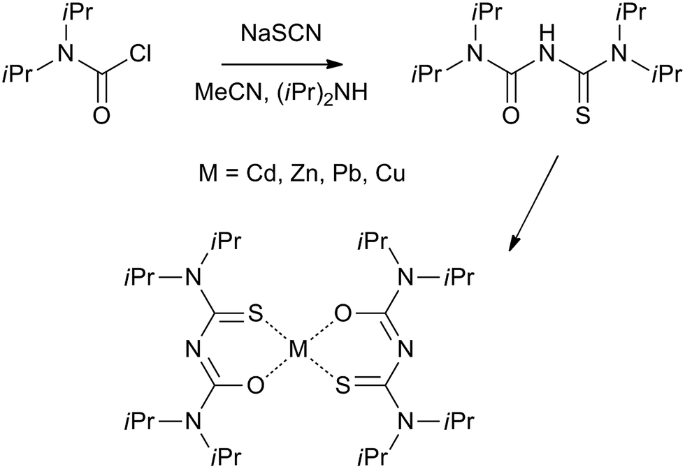 | ||
| Fig. 1 Synthesis of thiobiuret ligand and metal complexes. | ||
The reaction leading to nanocrystalline films taking place at the interface of water and toluene initially involves an exchange of anions. For example, in the case of CdS deposition:
| Cd[SON(CNiPr2)2]2(oil) + Na2S(aq.) → CdSinterface + 2Na[SON(CNiPr2)2](aq.) | (1) |
We confirmed the presence of Na(SON(CNiPr2)2)2 in water by electrospray ionization mass spectrometry. The seeds grow to a critical size and flocculate to form thin films. The mechanics of diffusion, heat flow, partition of ions and charges in the region surrounding the interface are all believed to be pertinent.5,6,31–34
Advances in the interfacial reaction scheme are hinged on the characteristics of the precursors used to deliver metal ions to the surface. Suitable precursors should be soluble in toluene or other mildly polar organic solvents, air stable, withstand contact with water and be able to release metal ions slowly to the interfacial region. Previous studies have mainly relied on strong bidentate ligands: cupferrates and thiocarbamates ligands to form sulfides.5 Thiobiurets used herein appear to readily fulfil these demanding criteria and indeed offer some advantages. Complexes of Cu, Sn, Co and Fe with either cupferrate and a variety of thiocarbamate ligands are poorly soluble in toluene whereas the corresponding thiobiurets are readily soluble. In the light of growing interest in sulfides of these metal ions, we envisage rapid developments in the area aided by the chemistry of thiobiurets.
3.2 Structure and morphology of the deposits
Scanning electron microscopic images reveal distinct microstructures for the deposits obtained (see Fig. 2). CdS and ZnS (Fig. 2a and b) consist of flattened aggregates that form a network of flocculates that span the entire imaged area. The longest dimension of the individual feature are between 100–300 nanometers. High resolution images reveal rough surfaces, indicating the presence of smaller constituent granules. In the case of PbS, spheroidal rather than flat features are seen. The microstructure of CuS films consist of curved egg-shell-like fragments that adorn a smooth background layer with nanoscopic voids (see Fig. 2c). It is clear that this structure is made up of nanoscopic grains.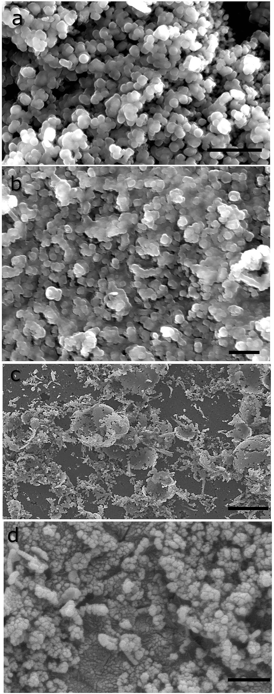 | ||
| Fig. 2 Scanning electron microscopic images of interfacial deposits of (a) ZnS obtained after 48 hours of growth at 60 °C, scale 2 μm; (b) CdS obtained at room temperature, 5 hours, scale 2 μm; (c) CuS obtained after 3 hours at 70 °C, scale 5 μm; (d) PbS, obtained after 2 hours at 50 °C, scale 1 μm. | ||
The grains making up the aggregates could be resolved by transmission electron microscopy (see Fig. 3). Dispersion by mild sonication is sufficient to break up the granular aggregates seen in Fig. 2. In the case of CuS, clumps of nanoparticles that form the aggregates are visible in the micrograph (Fig. 3c). High resolution images reveal lattice planes suggesting the particulates are indeed crystalline. The granules seen in Fig. 2 consist of tightly packed grains akin to a biscuit. We believe that the grains are protected against coalescence by a charged surface layer. The interfacial deposits are thus hierarchical mesoscalar assemblies of nanocrystals. Such structures involve self-assembly across multiple length scales and are difficult to obtain by other well-established techniques. However, these features seem to be commonly produced by interfacial deposition.5 We note that mesostructured assembly has been noted in interfacially-grown deposits of Pd,35 Bi2S3, Au34 and Ag.36 It is believed that such assembly is a direct manifestation of the forces at play at the oil–water interface.
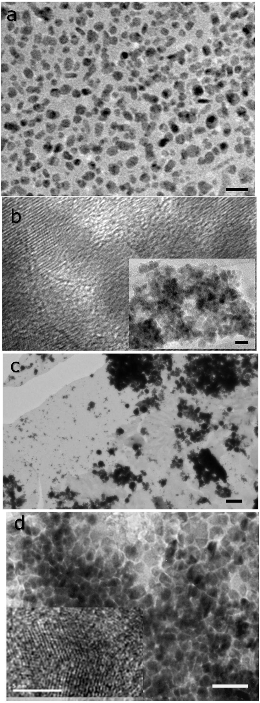 | ||
| Fig. 3 Transmission electron microscopic images of dispersed interfacial deposits of (a) ZnS obtained after 48 hours of growth at 60 °C, scale 15 nm; (b) CdS obtained at room temperature, 5 hours. The inset shows a low resolution image, scale 20 nm; (c) CuS obtained after 3 hours at 70 °C, scale 100 nm; (d) PbS, obtained after 2 hours at 50 °C, scale 25 nm, the inset shows a high resolution image with a scale bar measuring 5 nm. | ||
X-ray diffraction patterns of the deposits consists of broad peaks, characteristic of nanoscopic grains. In the case of CdS and ZnS, it is not possible to identify if the deposits are cubic or hexagonal owing to the width of the peaks and the similarities in the diffraction pattern of both these phases. Unambiguous assignment is however possible in the case of CuS, where the obtained pattern matches well with that expected of covellite (see Fig. 4). Notably, no other CuS phases are present. PbS deposits are cubic with a rock salt structure.
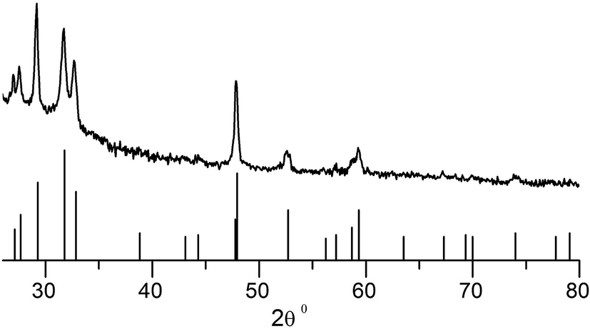 | ||
| Fig. 4 X-ray diffraction patterns of interfacial CuS deposit. Also shown are the peak position and intensity of the standard diffraction pattern corresponding to covellite (JCPDS no: 00-006-0464). The deposition was carried out for 6 hours with 0.078 mmol of Cu(SON(CNiPr2)2)2 in 30 mL of toluene and 30 mL equimolar aq. Na2S·9H2O at 70 °C. | ||
We note that the deposits obtained at the interface transfer well to glass substrates yielding films with uniform characteristics spread over areas of tens of square millimetres. It is possible to reliably measure physical properties of such films using thermally evaporated electrodes with 1 mm spacing between digits. The conductivity (σ) of CdS films grown at 40 °C over 24 h was found to be 1.31 × 10⁻⁶ Ω−1 m−1 at 280 K. ZnS films obtained under identical conditions were slightly less resistive, with σ of 1.75 × 10⁻⁶ Ω−1 m−1. The values compare well with those obtained from solution-deposited films of nanocrystals.37,38
Detailed transport measurements were carried out as a function of temperature for selected films. Films of CdS and ZnS nanocrystals obtained at 40 °C exhibit behaviour typical of semiconductors with a clear drop in conductivity with decreasing temperature. The drop in conductivity was 70% in the case of CdS films and a more modest 40% in the case of ZnS. The conductivity (σ) in these granular films can be analysed, following a model of activated hopping proposed by Neugebauer and Webb,39 according to which,
| σ ∝ e−2δβe−Ea/kT. | (2) |
| σ = Ae−Ea/kT. | (3) |
The activation energy depends on the diameter of the nanocrystalline grains as well as the dielectric properties of the nanocrystals and the surrounding medium.40,41 Plots of lnσ vs. 1/T were linear (see Fig. 5). Two distinct linear regimes are discernible in the plot corresponding to ZnS deposits (Fig. 5b) with the switch taking place around 200 K. Clearly the mechanism of conduction changes with the fall in temperature. We find no hysteresis in the behaviour suggesting that the change is reversible. Such behaviour has previously been attributed to changes in the film structure.42,43 An activation energy of 41.2 meV was obtained for the CdS deposits. In the case of ZnS, films Eas of 22.5 meV and 9.1 meV were obtained corresponding to the high (>200 K) and low (<200 K) temperature regimes. The Eas reported herein are in line with previous reports42,44 and suggest that charge transport is largely limited by the barrier present at the surface of the grains.
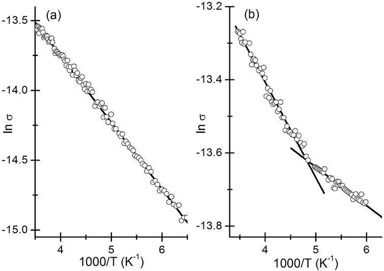 | ||
| Fig. 5 Plot showing linear relationship between σ and 1/T in the case of (a) CdS and (b) ZnS. Straight-line fits to the different σ regimes are shown. The units for σ are Ω−1 m−1. | ||
The composition and the surface structure of the deposits were analysed by X-ray photoelectron spectroscopy (XPS). Fig. 6 shows XPS of S 2p core levels of a nanocrystalline PbS deposit. The strong feature in the 159–164 eV binding energy (BE) range can be decomposed into two components S1 and S2. The former corresponds to S in PbS, while the smaller S2 component has several possible assignments. In studies of colloidal PbS NCs, it has been attributed to the surface S–C bond associated with the organic ligand.17,45 In our case, no passivating ligand is used, and the C 1s signal is of much lower intensity than is typical for colloidal NCs, but we cannot rule out the presence of small amounts of residual thiobiuret precursor. S2 has also been associated with sulfur atoms associated with one oxygen atom in surface –SO moieties,46 representing the very initial stages of oxidation. Its binding energy is also consistent with surface-adsorbed protons, in –SH species,47 which have also been proposed as intermediates formed in initial oxidation.48,49 The S 2p core level shows particularly large chemical shifts, such that any feature observed between ca. 165 eV and 171 eV may be attributed to oxidised species (such as sulfate and sulfite). The spectra were fitted with four doublet species corresponding to sulfur in PbS (S1), –SO/S–C/–SH (S2), sulfite and sulfate species (PbSOx) S3 and S4 respectively. In the light of the very low intensity of S3 and S4 species, it is apparent that very little surface reaction has taken place in the PbS deposits, despite a week of exposure to air. The distribution of surface oxidation products may be probed by varying the incident photon energy. The resulting change in photoelectron kinetic energy alters the photoelectron inelastic mean free path. The sampling depth from which 95% of the detected electrons originate is approximately 3 times the inelastic mean free path. Spectra were taken at multiple sampling depths by varying the energy of the incident X-ray beam between 300 and 800 eV to give sampling depths ranging between 2.0 nm and 5.1 nm (ref. 50) (Fig. 6). Very small features due to sulfate and sulfite are visible at the lowest sampling depth used (2 nm), indicating the presence of a very small amount of a sulfate/sulfite passivation layer,48 localised at the nanoparticle surfaces. This is in contrast to results obtained from colloidally-synthesised PbS nanoparticle samples which show a much larger degree of surface oxidation after a similar air exposure.17 The ratio of PbSOx:PbS as taken from the 2 nm sampling depth spectrum is approximately 0.02:1. This is 40 to 50 times less than for colloidally-synthesised nanoparticles,17 which showed PbSOx:PbS ratios in the range 0.8:1, 1.0:1 over similar sampling depths, after air exposure of only a few hours. The ability to produce such high quality deposits is a particularly noteworthy aspect of the interfacial deposition scheme. For PbS nanocrystals produced without a covering of organic ligands, such as those synthesised here, we expect the lowest energy surfaces to be the {100} surfaces8,51 so we associate this stability with the preferred (200) orientation typically found in XRD of these deposits.
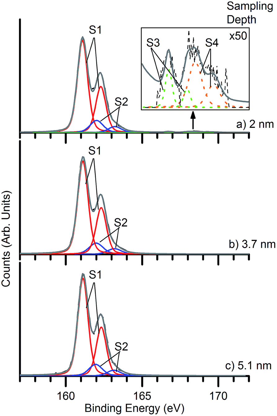 | ||
| Fig. 6 X-ray photoelectron spectra of a nanocrystalline PbS deposit exposed to air for approximately one week after synthesis. The spectra were obtained at sampling depths of (a) 2.0 nm (b) 3.7 nm and (c) 5.1 nm. Inset shows the signal due to oxidised sulfur species at 50× magnification. Peaks present are: S1 (red) sulfur present in PbS (lead sulfide), S2 (blue) –SO/S–C/–SH, S3 (green) sulfur present in PbSOx (sulfite), and S4 (orange) sulfur present in PbSOx (sulfate). | ||
3.3 Influence of deposition conditions
Deposition at the interface was carried out at different temperatures for varying lengths of time. The progress of the reaction was followed by monitoring the colouration of the interface. The properties of the deposits were ascertained under different conditions. The minimum temperature required to accomplish interfacial deposition, the maximum temperature studied as well as the pertinent times are summarized in Table 1. In all cases except CuS, good quality deposits can be obtained at room temperature (or below). No energy input is required during the reaction. This aspect is particularly attractive as other deposition methods nearly always require elevated temperatures. Our study adds to the growing body of evidence suggesting that interfacial deposition scheme is capable of producing quality nanocrystalline films at low temperatures.5,52 We envisage that thin films extending over larger areas can be obtained by increasing the interface area using a larger reaction vessel.| Deposit | Temperature (°C) | Time (h) | ||
|---|---|---|---|---|
| Min | Max | Onset | Saturation | |
| ZnS | RT | 70 | 1 | 24 |
| CdS | 10 | 70 | 0.5 | 48 |
| CuS | 50 | 70 | 1 | 12 |
| PbS | RT | 70 | 0.5 | 2 |
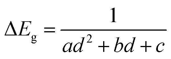
An increase in deposition temperature leads to quicker deposition and causes some changes to the morphology of the deposits. The most pronounced changes were seen in the case of CdS. Absorption of these films obtained at different temperatures consisted of a sharp onset, corresponding to optical band gaps higher than those of bulk CdS (see Fig. 7). The blue shift produced by size-dependent changes associated with nanocrystals fell from 0.55 eV to 0.15 eV (the onset/optical band gap decreased from 2.97 eV to 2.57 eV) as the temperature was raised from RT to 60 °C. The method proposed by Sarma and co-workers is used to relate the absorption features to the diameter of the particulates (d).53,54 This method, based on high level theoretical calculations yields accurate diameter estimates from the size-dependent shifts in band gap. Accordingly, the increase in band gap (ΔEg) is given by:
 | (4) |
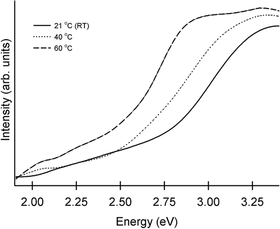 | ||
| Fig. 7 Absorption spectra of interfacial CdS films deposited on glass slides. The deposition temperature is indicated. The depositions were carried out for 24 hours. | ||
The conductivity of CdS films increases by two orders as the deposition temperature is raised to 60 °C (see Table 2). In the case of ZnS, a similar elevation produced minimal impact (Table 2). In chalcogenide films, variation in composition could lead to large changes.26 Here, elemental analysis by EDAX confirms that the metal:S ratio is 1:1 in the deposits produced at both the highest and lowest temperatures. Hence, we believe that larger grains lead to improved conductivity in the case of CdS. The small variation in case of ZnS is in line with expectations as grain size varies little with temperature in this system. An examination of changes accompanying elevated temperature offers justification for the grain size changes. It is reasonable to expect that higher temperatures lead to faster growth rates. This acceleration is tempered by increased solubility of precursors at high temperatures. The significance of the latter is more pronounced in the interfacial scheme where the concentrations employed are well below bulk saturation limits. Here, a small temperature effect indicating a close match between the two forces can be expected.5 If solubility has the upper hand, higher temperature deposits would be thinner. This seems to be the case for PbS, where higher temperatures lead to tangibly less intense colouration of the interface. In the case of ZnS and CdS, the measurements indicate a similar trend with thinner films being obtained at higher temperatures. In the light of ≈15 nm surface roughness present in these films, the variation in thickness is not significant. This is apparent in Fig. 7, where the absorption spectra of films grown at different temperatures reveal comparable optical densities at λmax. It is clear that deposition parameters have different impact on each of the systems. Further detailed studies relating the nature of the materials to the parameters are necessary to uncover factors that afford genuine control over morphology and grain size.
| Deposit | T (°C) | D (nm) | E g (eV) | σ (Ω−1 m−1) |
|---|---|---|---|---|
| CdS | 10 | 130 | 2.98 | — |
| CdS | RT | 124 | 2.97 | 9.03 × 10⁻⁷ |
| CdS | 40 | 122 | 2.75 | 1.31 × 10⁻⁶ |
| CdS | 50 | — | 2.75 | 7.23 × 10⁻⁶ |
| CdS | 60 | 110 | 2.57 | 6.31 × 10⁻⁵ |
| ZnS | RT | 130 | 3.58 | 1.58 × 10⁻⁶ |
| ZnS | 40 | 132 | 3.56 | 1.75 × 10⁻⁶ |
| ZnS | 60 | 124 | 3.55 | 2.15 × 10⁻⁶ |
Previously, a number of different copper sulfides including anilite (Cu7S4) and djurleite (Cu1.94S) have been obtained using 1,1,5,5-tetraisopropyl-2-thiobiuret ligand and deposition techniques such as aerosol assisted chemical vapour deposition.25 In an attempt to obtain other copper sulfides interfacial deposition was carried out with metal precursor to sodium sulfide concentration ratio ranging from 1:0.5 to 1:10 and at different temperatures. Remarkably, every one of these depositions yielded pure covellite (see Fig. 8). There is no notable difference in the X-ray patterns of the different samples obtained. Such robustness is particularly rare in the chemistry of copper sulfides where the richness of the phase diagram results in a mixture of products.56,57
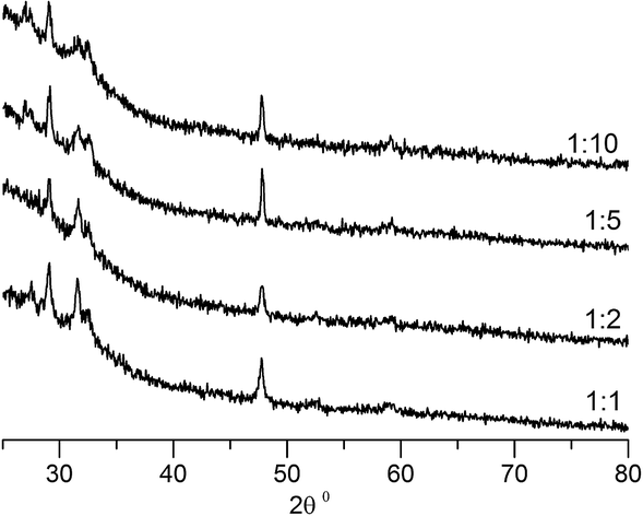 | ||
| Fig. 8 X-ray diffraction patterns of CuS deposits obtained with different copperthiobiuret:sodium sulfide molar ratios. The ratios are indicated alongside. The graphs have been shifted vertically for clarity. The depositions were carried out for 3 hours at 70 °C with 0.078 mmol of Cu(SON(CNiPr2)2)2 in 30 mL of toluene and 30 mL aq. Na2S·9H2O. | ||
Scanning electron microscopic images indicate that deposition at different precursor concentration ratios leads to different microstructures. Crucially, elemental analysis by EDAX confirms that the Cu:S ratio is 1:1 in the deposits. At ratios near 1:1, the deposits feature, in addition to the platelets, a number of other morphologies, prominent among which are whiskered outgrowths (see Fig. 9 and 2c). These features resembling flattened whiskers are several microns long and are typically about 100 nm wide. As the ratio is increased to 1:10, platelets and their globular aggregates replace the other morphologies. We believe that at low Cu:S ratios, the growth takes place near equilibrium conditions yielding two-dimensional modifications of the three dimensional hexagonal form in the shape of jagged features. At high Cu:S ratios, the growth is kinetically controlled leading to less well-defined (i.e. rounded) forms. It would be of interest to build on the excellent phase control offered by this technique and optimize parameters to yield specific morphologies. Research efforts are under way to address this challenge.
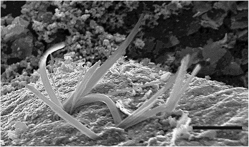 | ||
| Fig. 9 Scanning electron microscopic image of interfacial covellite deposit obtained using copperthiobiuret:sodium sulfide molar ratio of 1:5 scale bar is 5 μm. The deposition was carried out for 3 hours at 70 °C with 0.078 mmol of Cu(SON(CNiPr2)2)2 in 30 mL of toluene and 30 mL aq. Na2S·9H2O. | ||
4 Conclusions
Nanostructured films of CdS, ZnS, CuS and PbS have been obtained at the interface of water and toluene by using [M(SON(CNiPr2)2)2], (M = Cd, Zn, Pb or Cu) in toluene as source of metal ions. All deposits adopt mesostructured forms with superstructure features in the range of 100s of nanometres made up of grains with dimensions less than 10 nm. It is possible, in the case of CdS, to tune the grain size in the range of 4 to 7 nm by varying the deposition conditions. Charge transport in CdS and ZnS films takes place by an activated hopping mechanism with activation energies of the order of tens of meV. Two particularly noteworthy aspects of this study are the excellent phase control provided by the [Cu(SON(CNiPr2)2)2] precursor for the deposition of CuS and the ability to produce PbS with greatly reduced surface oxidation levels. We believe that this first report featuring air and water stable, highly soluble thiobiuret precursors will pave way for rapid development of the interfacial deposition technique. We have ascertained that it is possible to deposit other nanocrystalline films such as ZnO using the thiobiuret precursors. Further research into these aspects is under way.Acknowledgements
The authors thank the Royal Society and The Leverhulme trust for funds. The experimental work at Elettra was funded under The European Community's Seventh Framework Programme (FP7/2007-2013) under grant agreement no. 226716 and by EPSRC travel grant EP/H0020446/1.References
- G. Konstantatos and E. H. Sargent, Nat. Nanotechnol., 2010, 5, 391 CrossRef CAS PubMed.
- Semiconductor Nanocrystal Quantum Dots: Synthesis, Assembly, Spectroscopy and Applications, ed. A. Rogach, Springer, 2008 Search PubMed.
- M. Liong, J. Lu, M. Kovochich, T. Xia, S. G. Ruehm, A. E. Nel, F. Tamanoi and J. I. Zink, ACS Nano, 2008, 2, 889 CrossRef CAS PubMed.
- Y. Gao and Z. Tang, Small, 2011, 7, 2133 CrossRef CAS PubMed.
- P. J. Thomas, E. Mbufu and P. O'Brien, Chem. Commun., 2013, 49, 118 RSC.
- C. N. R. Rao and K. P. Kalyanikutty, Acc. Chem. Res., 2008, 41, 489 CrossRef CAS PubMed.
- C. N. R. Rao, G. U. Kulkarni, V. V. Agrawal, U. K. Gautam, M. Ghosh and U. Tumurkar, J. Colloid Interface Sci., 2005, 289, 305 CrossRef CAS PubMed.
- D. Fan, P. J. Thomas and P. O'Brien, J. Am. Chem. Soc., 2008, 130, 10892 CrossRef CAS PubMed.
- S. N. Mlondo, E. M. Andrews, P. J. Thomas and P. O'Brien, Chem. Commun., 2008, 2768 RSC.
- D. Fan, P. J. Thomas and P. O'Brien, Chem. Phys. Lett., 2008, 465, 110 CrossRef CAS PubMed.
- J. E. Oliver, S. C. Chang, R. T. Brown and A. B. Borkovec, J. Med. Chem., 1971, 14, 773 CrossRef.
- W. O. Foye and J. J. Hefferren, J. Am. Pharm. Assoc., 1953, 42, 31 CrossRef CAS PubMed.
- F. Kurzer, Chem. Rev., 1956, 56, 95 CrossRef CAS.
- K. Ramasamy, M. A. Malik, P. O'Brien and J. Raftery, Dalton Trans., 2010, 39, 1460 RSC.
- F. W. Wise, Acc. Chem. Res., 2000, 33, 773 CrossRef CAS PubMed.
- A. J. Nozik, M. C. Beard, J. M. Luther, M. Law, R. J. Ellingson and J. C. Johnson, Chem. Rev., 2010, 110, 6873 CrossRef CAS PubMed.
- S. J. O. Hardman, D. M. Graham, S. K. Stubbs, B. F. Spencer, E. A. Seddon, H.-T. Fung, S. Gardonio, F. Sirotti, M. G. Silly, J. Akhtar, P. O'Brien, D. J. Binks and W. R. Flavell, Phys. Chem. Chem. Phys., 2011, 13, 20275 RSC.
- A. J. Nozik, Chem. Phys. Lett., 2008, 457, 3 CrossRef CAS PubMed.
- Q. Shen, K. Katayama, T. Sawada, S. Hachiya and T. Toyoda, Chem. Phys. Lett., 2012, 542, 89 CrossRef CAS PubMed.
- C. Wu, S.-H. Yu and M. Antonietti, Chem. Mater., 2006, 18, 3599 CrossRef CAS.
- J.-J. Wang, D.-J. Xue, Y.-G. Guo, J.-S. Hu and L.-J. Wan, J. Am. Chem. Soc., 2011, 133, 18558 CrossRef CAS PubMed.
- T. Todorov, K. Reuter and D. Mitzi, Adv. Mater., 2010, 22, E156 CrossRef CAS PubMed.
- M. G. Panthani, V. Akhavan, B. Goodfellow, J. P. Schmidtke, L. Dunn, A. Dodabalapur, P. F. Barbara and B. A. Korgel, J. Am. Chem. Soc., 2008, 130, 16770 CrossRef CAS PubMed.
- M. E. Fleet, Rev. Mineral. Geochem., 2006, 61, 365 CrossRef CAS.
- A. L. Abdelhady, K. Ramasamy, M. A. Malik, P. OB́rien, S. J. Haigh and J. Raftery, J. Mater. Chem., 2011, 21, 17888 RSC.
- D. J. Vaughan and J. R. Craig, Mineral Chemistry of Metal Sulfides, Cambridge University Press, Cambridge, 1978, p. 290 Search PubMed.
- S. W. Goh, A. N. Buckley and R. N. Lamb, Miner. Eng., 2006, 19, 204 CrossRef CAS PubMed.
- A. Aguiar, C. Lima, Y. Yadava, L. Tellez, J. Ferreira and E. Montarroyos, Phys. C, 2000, 341, 593 CrossRef.
- W. Liang and M. H. Whangbo, Solid State Commun., 1993, 85, 405 CrossRef CAS.
- M. T. S. Nair and P. K. Nair, Semicond. Sci. Technol., 1989, 4, 191 CrossRef CAS.
- I. Benjamin, Chem. Rev., 2006, 106, 1212 CrossRef CAS PubMed.
- G. Luo, S. Malkova, J. Yoon, D. G. Schultz, B. Lin, M. Meron, I. Benjamin, P. Vanysek and M. L. Schlossman, Science, 2006, 216, 311 Search PubMed.
- A. Boker, J. He, T. Emrick and T. P. Russell, Soft Matter, 2007, 3, 1231–1248 RSC.
- C. N. R. Rao, G. U. Kulkarni, P. J. Thomas, V. V. Agrawal and P. Saravanan, J. Phys. Chem. B, 2003, 107, 7391 CrossRef CAS.
- L. Z. Zheng and J. H. Li, J. Phys. Chem. B, 2005, 109, 1108 CrossRef CAS PubMed.
- V. V. Agrawal, P. Mahalakshmi, G. U. Kulkarni and C. N. R. Rao, Langmuir, 2006, 22, 1846 CrossRef CAS PubMed.
- N. Y. Morgan, C. A. Leatherdale, M. Drndić, M. V. Jarosz, M. A. Kastner and M. Bawendi, Phys. Rev. B: Condens. Matter Mater. Phys., 2002, 66, 075339 CrossRef.
- S. Eitssayeam, U. Intatha, K. Pengpat and T. Tunkasiri, J. Mater. Sci., 2005, 40, 3803 CrossRef CAS.
- C. A. Neugebauer and M. B. Webb, J. Appl. Phys., 1962, 33, 74 CrossRef CAS PubMed.
- R. P. Andres, J. D. Bielefield, D. B. Janes, V. R. Kolagunta, C. P. Kubiak, W. J. Mahoney and R. G. Osifchin, Science, 1996, 273, 1 CrossRef.
- W. P. Wuelfing, S. J. Green, J. J. Pietron, D. E. Cliffel and R. W. Murray, J. Phys. Chem. C, 2008, 112, 12507 Search PubMed.
- N. J. Hardy, M. D. Hanwell and T. H. Richardson, J. Mater. Sci.: Mater. Electron., 2007, 18, 943 CrossRef CAS.
- G. L. Stansfield and P. J. Thomas, J. Am. Chem. Soc., 2012, 134, 11888 CrossRef CAS PubMed.
- M. S. Kang, A. Sahu, D. J. Norris and C. D. Frisbie, Nano Lett., 2010, 10, 3727 CrossRef CAS PubMed.
- J. Tang, L. Brzozowski, D. A. R. Barkhouse, X. H. Wang, R. Debnath, R. Wolowiec, E. Palmiano, L. Levina, A. G. Pattantyus-Abraham, D. Jamakosmanovic and E. H. Sargent, ACS Nano, 2010, 4, 869–878 CrossRef CAS PubMed.
- L. V. Yashina, A. S. Zyubin, R. Puttner, T. S. Zyubina, V. S. Neudachina, P. Stojanov, J. Riley, S. N. Dedyulin, M. M. Brzhezinskaya and V. I. Shtanov, Surf. Sci., 2011, 605, 473–482 CrossRef CAS PubMed.
- A. J. Leavitt and T. P. Beebe, Surf. Sci., 1994, 314, 23–33 CrossRef CAS.
- D. Cant, K. Syres, P. Lunt, H. Radtke, J. Treacy, P. Thomas, E. Lewis, S. Haigh, P. O'Brien, K. Schulte, F. Bondino, E. Magnano and W. Flavell, Langmuir, 2015, 31, 1445 CrossRef CAS PubMed.
- D. Fornasiero, F. S. Li, J. Ralston and R. S. C. Smart, J. Colloid Interface Sci., 1994, 164, 333–344 CrossRef CAS.
- S. Tanuma, C. J. Powell and D. R. Penn, Surf. Interface Anal., 1991, 17, 927 CrossRef CAS PubMed.
- Z. W. Wang, C. Schliehe, T. Wang, Y. Nagaoka, Y. C. Cao, W. A. Bassett, H. M. Wu, H. Y. Fan and H. Weller, J. Am. Chem. Soc., 2011, 133, 14484–14487 CrossRef CAS PubMed.
- S. N. Mlondo, P. J. Thomas and P. O'Brien, J. Am. Chem. Soc., 2009, 131, 6072 CrossRef CAS PubMed.
- R. Viswanatha and D. D. Sarma, Chem.–Eur. J., 2006, 12, 180 CrossRef CAS PubMed.
- S. Sapra and D. D. Sarma, Phys. Rev. B: Condens. Matter Mater. Phys., 2004, 69, 125304 CrossRef.
- D. Fan, P. J. Thomas and P. O'Brien, J. Mater. Chem., 2007, 17, 1381 RSC.
- G. Henshaw, I. P. Parkin and G. A. Shaw, J. Chem. Soc., Dalton Trans., 1997, 231 RSC.
- S. Gorai, D. Ganguli and S. Chaudhuri, Cryst. Growth Des., 2005, 5, 875 CAS.
| This journal is © The Royal Society of Chemistry 2015 |