Matteo Bosi
IMEM-CNR, Parco Area delle Scienze 37A, 43124 Parma, Italy. E-mail: bosi@imem.cnr.it
First published on 10th August 2015
Nanosheet materials such as graphene, boron nitride and transition metal dichalcogenides have gathered a lot of interest in recent years thanks to their outstanding properties and promises for future technology, energy generation and post-CMOS device concepts. Amongst this class of materials transition metal dichalcogenides based on molybdenum, tungsten, sulfur and selenium gathered a lot attention because of their semiconducting properties and the possibility to be synthesized by bottom up techniques. Vapour phase processes such as chemical vapour deposition permit to produce high quality layers and to precisely control their thickness. In order to target industrial applications of transition metal dichalcogenides it is important to develop synthesis methods that allow to scale up wafer size, and eventually integrate them with other technologically important materials. This review will cover all the currently proposed methods for the bottom up synthesis of transition metal dichalcogenides from the vapour phase, with particular emphasis on the precursors available and on the most common semiconductor techniques like metal organic chemical vapour deposition and atomic layer epitaxy. A summary of the most common characterization technique is included and an overview of the growth issues that still limit the application of TMD is given.
Amongst all the proposed solutions, graphene is the one that attracted most attentions.5 Its exceptional mechanical, electronic, optical and transport properties have promoted a lot of fundamental and applied research, resulting in a nobel prize assignment and in the development of new physics. Its carriers have mobility of 106 cm2 V−1 s−1 and are Dirac fermions with zero effective mass, making possible to study phenomena related to the quantum mechanics theory in a condensed-matter playground. Integrated circuits based on graphene transistor were demonstrated and high-frequency operation up to gigahertz was proven.6 Graphene functionalization permitted to realize novel chemical and biological sensors7 and is also being considered for hydrogen conversion and storage.8
Despite all these opportunities, graphene has several major drawbacks such as the lack of an electronic bandgap that makes certain kind of applications, for instance logic circuits, very difficult to develop: a graphene transistor cannot have the two conventional on and off states, it cannot be completely switched off, it has more energy leakage and produces more heat. Bandgap opening is possible through bandgap engineering (by nanostructuring, chemical functionalization or by applying a high electric field) but this step adds another level of complexity and degrades material properties. Graphene intrinsic defects and the presence of surface adatoms degrades the carrier mobility. Moreover it is chemically inert and functionalization, necessary to make it reactive to selected molecules, results in loss or degradation of several of its properties. These drawbacks fostered the research on alternative materials with similar structure and characteristics.
There is a wide variety of materials that can be thinned down to monolayer like graphene, exhibiting strong in-plane bonds and weak interplane interaction. The list includes transition metal dichalcogenides (TMD), silicene,9 germanene10 and boron nitride.11 The properties of these materials depend on their dimension rather than their lateral size and, due to their novelty and excellent electronic properties, they are considered an exiting field for new research.
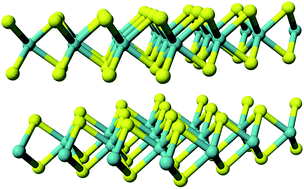
TMD are materials with chemical formula MX2, where M is a transition metal of group 4–10 (Nb, Ta, Mo, W, etc.) and X a chalcogen such as S, Se, Te. They are studied since long time and, in bulk form, were grown since 1970.12–15 The typical crystal structure (Fig. 1) consists in a stack of a transition metal layer between two chalcogen layers and it can be described as a van der Waals solid with strong (covalent) bonds in 2D plane, while the interaction between different planes is much weaker. Their symmetry is hexagonal or rhombohedral, with atoms arranged in octahedral or trigonal prismatic coordination.
TMD bulk material can be exfoliated with different methods such as scotch tape,16 solvents17 or lithium intercalation.18 More than 40 combinations of M and X were observed,19 with very different characteristics and a large range of electronic properties from metallic to semiconducting to superconducting. Bulk properties differ significantly from the ones of low dimensional, few layer stacks of TMD: for example the bandgap may change from indirect (bulk) to direct (monolayer), resulting in strong enhancement of optical absorption and emission.20 When TMD are thinned down to monolayers, they have the same honeycomb structure of graphene and posses very similar properties, but the most important difference is that they exhibit a finite direct bandgap, from 1 to 2 eV, making 2D TMD ideal candidates for electronic devices, logic circuits, detectors, optoelectronic, photovoltaic, energy storage and catalytic applications.21
Novel properties are observed in monolayer TMD, such as valley polarization: conduction and valence bands of TMD monolayers present two inequivalent valleys at points K and K0, giving a new degree of freedom to carriers. New device concepts can be based on valleytronics, addressing the carriers by their valley index and permitting a control of information using circular polarized light.22 Moreover, spin–valley coupling may occur, offering a feature that may lead to completely new device design.23
TMD electronic and semiconducting properties (Table 1) make them ideal candidates for the realization of digital electronic devices, FET and transistor, with the possibility to achieve high on/off current ratio.24 Important milestones were achieved with TMD, such as the development of a top-gated MoS2 FET with mobility of 60–70 cm2 V−1 s−1 and on/off ratio of 108 at room temperature,25 inverters with gain between 2 and 16,26,27 phototransistors and photosensors,28,29 gas and biological sensors.30 The trend is now to integrate different building blocks into a single device and to fabricate high performance CMOS based circuits.31
Material | Type | Monolayer bandgap (eV) | Mobility (cm2 V−1 s−1) |
---|---|---|---|
Graphene | Semi metallic | — | 2 × 10⁵ |
Silicene | Semi metallic | — | 1 × 10⁵ (theory) |
Germanene | Semi metallic | — | 1 × 10⁵ (theory) |
BN | Insulating | 5.2 | |
MoS2 | Semiconducting | 1.8 | 200 (Monolayer) |
MoSe2 | Semiconducting | 1.5 | 50 (exfoliated) |
MoTe2 | Semiconducting | 1.1 | 50 (bulk) |
WS2 | Semiconducting | 1.9–2.1 | 100–200 (bulk) |
WSe2 | Semiconducting | 1.7 | 100–500 (bulk) |
WTe2 | Semiconducting | 1.1 | 20 (bulk) |
TaS2 | Metallic super conducting | — | |
TaSe2 | Metallic super conducting | — | |
NbS2 | Metallic super conducting | — | |
NbSe2 | Metallic super conducting | — |
The continuous advance of personal portable devices, smartphones over all, is pushing researchers to develop flexible high performance electronics. Low dimensional materials such as graphene and TMD have high mechanical strength and can be deformed up to 10% before breaking and, thanks to the low dimensionality, they can be deposited or transferred on flexible substrates: this makes TMD ideal candidates for the next generation of portable devices and indeed the first demonstration of flexible devices with these materials already occurred.32,33
Nowadays most of the optoelectronic devices are made from III–V and III–N compounds. Their great success is due to the possibility to form ternary compounds such as InxGa1−xAs, InxGa1−xN, AlxGa1−xAs etc. with different composition. It is thus possible to fabricate lattice matched and mismatched heterostructures, to tune the bandgap, optical emission, absorption, electron properties, etc., and to realize complex devices such as LED, solar cells, photodetectors. TMD and 2D nanosheets such as graphene and boron nitride can be considered as a new class of materials that in principle would permit to obtain ternary compounds and stacked layers similar to the one realized for III–V compounds. Theoretical models predict that mix of TMD is thermodynamically stable34 and the bandgap of a ternary alloy can be continuously tuned.35,36 Stacks of exfoliated 2D material were combined to realize LED by van der Waals heterostructures.32
Most of TMD devices developed so far were realized from mechanically exfoliated sheets. Although flakes quality is very high and excellent proof of concepts may be obtained in this way, the method pose critical limits on large scale production. In order to target TMD industrial applications it is mandatory to develop reliable and high-throughput deposition techniques on large area substrates, and compatibility with the current systems and processes could be a tremendous added value. Control of the precursors flow in the vapour phase through the use of gases or controlled evaporation of liquid precursors would permit to increase deposition reproducibility. Chemical vapour deposition (CVD) and atomic layer deposition (ALD) are nowadays the most used processes to realize almost all kind of electronic devices with the current used materials (Si, Ge, III–V, III–N, oxides, etc.): it would be highly desirable to develop TMD synthesis processes that share the same deposition equipments used for other compounds, since it could open the possibility to directly integrate TMD with other materials.
Not all TMD are technologically interesting, since most of them are not stable in standard conditions and reacts rapidly with atmosphere, losing their peculiar properties. The most promising, and the ones on which this review will focus, are MoS2, MoSe2, WS2 and WSe2, thanks to their peculiar electronic, optical and chemical properties and the possibility to synthesize them by bottom up techniques.
Several papers were already published on the most important properties, applications and synthesis of TMD19,37–41 but a comprehensive review on the different vapour phase deposition techniques, in particular with focus on CVD and ALD has not been proposed, yet.
An analysis of the growth methods, processes and precursors for this novel class of 2D materials is extremely important in order to understand the best routes to obtain the highest quality material and the most feasible way to realize TMD nanosheets. For example, the controlled and reproducible synthesis of monolayer TMD with low defects and crystallinity, the deposition scalability to large area, the fabrication of TMD heterostructures and the possibility to integrate them with other materials are still open issues to be addressed. Providing technological solutions for the growth of TMD would pave way towards the realization of new applications and device based on these materials.
Raman spectroscopy and photoluminescence are considered the most useful and reliable techniques to identify the numbers of layer in both exfoliated and synthesized TMD. Optical interference and Atomic Force Microscopy (AFM) are also used to exactly determine the layer numbers but, although they can provide precise results, they have limited throughput and are more time consuming. In order to develop synthesis on large area substrates and to target mass production, fast and reliable characterization techniques are needed, and Raman and PL can successfully meet these requirements.
Raman spectroscopy is considered a powerful tool to determine the number of layers: the vibrational modes of TMD flakes are strongly influenced by the thickness, since any additional layer beyond the first interacts with the bottom layer and change energy, width and amplitude of the peaks.45 Only two peaks are usually permitted in Raman backscattering geometry of few-layers TMD, namely E12g and A1g, related to the in-plane and out-of-plane vibrations of M and X atoms, respectively. As the layer number increase, the out of plane vibrations A1g are dampened, leading to a blue shift. The E12g peak, instead, undergoes a red shift due to the relaxation of in-plane phonon modes. Moreover, A1g modes are sensitive to carrier density and doping, resulting in red shift and peak broadening, respectively.24 Table 2 summarizes the expected Raman peak position of bulk and monolayer TMD.
One of the most important characteristics of monolayer TMD is the strong enhancement of PL signal with respect to bulk emission.20 As discussed in the previous section, bulk TMD are indirect bandgap materials: the indirect bandgap is due to a transition from the top of the Γ point valence band to the bottom of the conduction band, between Γ and K point. As the number of layers decrease down to one, the indirect bandgap energy increases and cross the direct gap, that remains in the same position. This is the reason for the strong enhancement of the emission signal, up to 10–20×, coupled to a peak blue shift (Table 3). Thanks to micro-PL mapping, different zones of a single flake can be analyzed in order to identify defects or the presence of additional layers.
There are basically two top down strategies adopted: mechanical exfoliation through Scotch tape and liquid methods, which can be subsequently divided in two categories: lithium intercalation and solvent-assisted sonication.
Since most TMD, and in particular MoS2, MoSe2,WS2 and WSe2, are available in bulk form, single layers can be exfoliated using the Scotch tape methods, similarly to what is done on graphene. Exfoliated flakes up to 10 μm wide and high crystallinity can be obtained and are usually identified using optical microscopy, considering the color contrast given by layers with different thicknesses on SiO2 (Fig. 2).49 However, despite these results, the scale up of Scotch tape method is extremely difficult and the throughput is very limited.
![]() | ||
Fig. 2 Optical and atomic force microscopy images of dichalcogenide nanolayers deposited on 270 nm SiO2 with corresponding contrast and height profiles of monolayers: (a)–(c) for MoS2, (d)–(f) for WSe2 and (g)–(i) for NbSe2. Contrast and height profiles of monolayer flakes are taken across the black lines drawn on optical images, and red lines on AFM images. Measured thicknesses correspond well with interlayer distances in dichalcogenide crystals. Observed optical contrast is in the 25–30% range for MoS2 and WSe2 and is slightly lower that the values predicted in the model. In the case of NbSe2 optical contrast is in the 5–10% range.49 © IOP Publishing. Reproduced with permission. All rights reserved. |
TMD can be exfoliated by ultrasonic treatment in appropriate solvents or by using surfactants (Fig. 3):17 sonication usually results in crystal flakes with dimension of a few hundreds nanometers50,51. A more viable solution is to utilize lithium containing compounds that intercalate into atomical layers, followed by a reaction in water, that separates the sheets by producing H2.18,52 Although exfoliation in liquid permits to obtain high yield of monolayers dispersed in a solution that can be adopted for applications such as electrochemical energy storage, catalysis, sensing, in ink-jet printing or to prepare composites and hybrids by mixing different solutions with different materials, its main disadvantages are the small size of the obtained flakes, that can limit some applications where large area flakes or films are needed. The challenges to be addressed are the yield enhancement of single layers (most of the flakes are few-layers) and the control of the lateral dimensions of the exfoliated sheets.
Since this review will mainly focus on gas phase methods, the reader is addressed to other reviews for details about the above cited top down methods. For example MoS2, MoSe2, WS2, NbSe2, WSe2, VSe2 and MoTe2 obtained by mechanical exfoliation are reported in ref. 53–57; a comprehensive list of solvents used for the liquid exfoliation is cited in ref. 50 while lithium intercalation is discussed in ref. 58 and 59.
Most of the proposed processes utilize one or two of the TMD constituent elements (metal and sulfur/selenium) in vapour form, transporting the selected species over the substrate with a carrier gas. This permit, in principle, to achieve a good control over the gas composition and, through flowdynamic optimizations obtained with chamber/tube design, to deliver the precursors in a homogeneous way over all the substrate area: large area scalability, uniformity and thickness control are routinely achieved for thin films deposited by CVD and can potentially be obtained also for monolayer TMD.
CVD is a widely used technique in material science and it is commonly employed to deposit a large class of semiconductors, metals, oxides, etc. on a variety of substrates. Only recently it was applied for the synthesis of low dimensional materials, such as graphene and TMD. Li et al.60 were the first to demonstrate large scale deposition of graphene utilizing methane on copper foil and later a variety of papers followed on TMD and boron nitride nanosheets.
Depending on the particular setup, the gas flow can be carefully controlled through the chamber design and a good flowdynamic optimization can, in principle, guarantee an efficient transport of species, good homogeneity, easily scale up to large area and excellent reproducibility. For these reasons CVD is one of the most promising techniques to synthesize monolayers TMD on large area with controlled thickness, good crystallographic quality and excellent electronic properties.
ALD is a modified CVD technique in which the two precursors are delivered separately in the growth chamber. It was invented by T. Suntola in 1974 (ref. 61) and was originally used to deposit ZnS film for electroluminescent devices. ALD is nowadays very common for oxides growth and for conformal deposition on nanostructures, patterned substrates, high aspect ratio structures such as trenches or pillars, etc., and it is largely used for the deposition of high-k oxides.
A single ALD growth cycle consists in: injection of precursor 1, purge with inert gas, injection of precursor 2, purge with inert gas. Excess reactants and reaction by-products are evacuated during purge cycles and the surface reactions during precursors supply are self-limited: if the substrate surface is sufficiently reactive to the precursor and if the precursor does not bond with itself, one ALD growth cycle should in principle deposit a single monolayer of the selected specie: uniform films with excellent conformality can be thus deposited even onto complex-shaped large area substrates. For this reason, ALD should be considered as one of the most promising technique for the deposition of TMD, because theoretically it would permit to tailor the number of deposited layers by defining the number of cycles. Despite its potential, ALD is still not so widespread for TMD, mainly because of a lack of suitable chemistry.62 Nevertheless, several groups used ALD also for the deposition of metals or metal oxides of controlled thickness to be further sulfurized or selenized by other techniques.
Before discussing the details of the different synthesis procedures, it is to be noted that most of these techniques share common precursors: it is thus very important to understand which kind of chemicals are available for TMD CVD and their physical properties. Beside the most commonly used S or Se powders or H2S gas for chalcogens, there are also less common chemicals worth to be mentioned. Also, M or MOx may be deposited on a substrate for further selenization/sulfurization: knowledge on how to control their deposition is often mandatory to obtain monolayer TMD.
The following section will exhaustively discuss the precursors used for TMD synthesis by CVD. To the best of author's knowledge this summary was never proposed before. The main focus will be on S, Se, Mo and W because MoS2, MoSe2, WS2 and WSe2 are considered to be the most technologically relevant compounds for the realization of devices.
S powder melts at 115 °C and evaporates to gaseous sulfur, with vapour pressure reported in Fig. 4: knowing the value of this parameter permits, in principle, to get a better control of the gas phase and to deliver a controlled quantity of precursor towards the substrate. However, the quantity of vapourized sulphur depends also on the mass of powder put in the crucible: for this reason the use of powders as main reagents, even if it is very common due to its simplicity, may pose some problems for reproducibility and control of the deposited layers.
![]() | ||
Fig. 4 Sulfur vapour pressure vs. temperature (adapted from ref. 63). |
Limit (ppm) | |
---|---|
Short-term exposure limit (STEL) | 15 |
Immediately dangerous to life and health (IDLH) | 100 |
For all these reasons, special care should be taken to design a reactor with H2S line64 and it is not so commonly used for the synthesis of TMD but, despite safety drawbacks, several research groups utilize it because the delivery of a gas to the growth chamber is much more controllable than evaporation of solid sources, ensuring higher reproducibility of the process.
Thanks to its fast decomposition at high temperature, H2S should be more efficient that elemental S in the growth of TMD, and should help in improving uniformity.65 Partial pressure of H2S in the gas phase during TMD growth is usually in the range 10−1 to 10−2.66,67 H2S may also act as reducing agent for metal oxides.
Brooks69 studied the vapour pressure of solid selenium with quartz Boudon gages, reported in Fig. 5.
![]() | ||
Fig. 5 Selenium vapour pressure (adapted from ref. 69). |
Limit (ppm) | |
---|---|
8 hour period | 0.05 |
Immediately dangerous to life and health (IDLH) | 100 |
However, like H2S, the odor in concentrations below 1 ppm rapidly disappears because of olfactory fatigue.
MSDS of this compound reports that it is deadly poison by inhalation and a very poisonous irritant to skin, eyes, and mucous membranes. It may also cause central nervous system effects. It has been found that repeated exposures to concentrations of 0.3 ppm are fatal to experimental animals by causing a pneumonitis and injury to liver and spleen.
Due to its high toxicity and the ready availability of safer alternatives, H2Se is usually not used for the synthesis of TMD, even if it can react with W to form WSe2 according to the reaction (1):70
![]() | (1) |
Bozheyev et al.71 have used H2Se as a selenization agent to prepare WSe2 thin films 600 nm thick, starting from selenium-rich WSe2−x deposited by reactive magnetron sputtering but, at the best of author knowledge, no other paper was found employing H2Se for nanosheet TMD synthesis.
The synthesis of WSe2 was carried out via metal organic chemical vapour deposition (MOCVD) using tungsten hexacarbonyl W(CO)6 and dimethyl selenide (CH3)2Se as the W and Se sources.72 Dimethyl selenium is a stable colourless liquid with an unpleasant odour, which hydrolyzes in water and reacts violently with acids and strong oxidizing agents. Its boiling point is 56–58 °C so it can be conveniently used in a MOCVD system. Its vapour pressure was determined by Karlson et al.73 and reported in Fig. 6.
![]() | ||
Fig. 6 Vapour pressure of DMSe and DMDSe (adapted from ref. 73). |
Film quality and carbon contamination depends strongly on (CH3)2Se purity: 99.99% pure (CH3)2Se performs better than 99% pure precursor.72
Diethyl selenide is another metal organic compound that was used to grow WSe2 thin films74 but not yet used for the synthesis of nanosheet TMD. It was heated to 60 °C and delivered to the growth chamber by N2. Its vapour pressure was studied by Tanaka et al.75 It should be noted that chemical reaction of WSe2 and diethyl selenide could produce H2Se, so waste gas must be properly handled.
Di-tert-butylselenide and diethylselenide were used by Boscher et al. to deposit MoSe2 films using MoCl5 as the other precursor74 and VSe2 using VCl4 and VOCl3.76 In these works the focus was on thin film and not on monolayers: no other paper was found, on the best of author knowledge, about the use of these precursors for 2D TMD.
Evaporation of liquids, solids or metal-organic Mo compounds such as MoCl5, MoF6, Mo(CO)6 could be one of the most straightforward methods to integrate Mo into a standard CVD system and to obtain good reproducibility and homogeneity over a large area.
MoO3 is produced either by heating MoS2 or by acidification of aqueous solutions of sodium molybdate with perchloric acid according to the reaction (2):77
![]() | (2) |
MoO3 powders are available with purity up to 99.98%. The vapour pressure of MoO3 is reported in Fig. 7.
![]() | ||
Fig. 7 Vapour pressure of MoO3, adapted from ref. 78. |
Several techniques are used to deposit a thin Mo film onto a variety of substrates (Si, SiO2, sapphire, Cr, Au, etc.), the most common being e-beam evaporation and sputtering. The thickness of the deposited layer is usually monitored through a quartz microbalance.
An alternative starting layer is MoO3 deposited by evaporation,79 because this oxide has a lower evaporation temperature with respect to Mo and it is more easily sulfurized/selenized. In order to increase reliability and control over the number of Mo layers, several groups used ALD with different kind of precursors: this is in principle the best technique control the thickness. There are different precursors available for CVD deposition of either Mo or MoO3 layers, which will be discussed in the following paragraphs.
Diskus et al.80 used Mo(CO)6 to deposit MoO3 layers on single crystalline Si(111) and soda lime glass. Mo(CO)6 was kept at room temperature and delivered to the growth chamber with the use of N2. An onset decomposition of 163 °C was determined for Mo(CO)6. After 1000 cycles the film thickness was between 35 and 75 nm: fine control over layer thickness can thus in principle be obtained.
1–50 mg of MoCl5 are generally used as powders for the growth of MoS2 along with S powders82,83 but MoCl5 is also used for the ALD of MoS2 with H2S as the other precursor.84 For the ALD process, in order to have a suitable vapour pressure, MoCl5 source was kept at 120 °C.
It was used as precursor for ALD of atomic Mo layers with Si2H6 as the other reactant.85 It was also used to deposit thin films of MoS2 by CVD using H2S as the other precursor86,87 but no reports about the direct synthesis of low dimension TMD were found in literature.
Bis(tert-butylimido)-bis(diethylamido)molybdenum[(tBuN)2Mo(NEt2)2] and bis(tert-butylimido)-bis(di-isopropylamido)molybdenum [(tBuN)2Mo(NiPr2)2 were used for ALD of molybdenum nitrides88 but no evidence of a suitable chemistry was found for sulfide/selenide compounds.
![]() | ||
Fig. 8 WO3 vapour pressure, adapted from ref. 97. |
WCl6, kept at 100 °C in a stainless steel bubbler, was used for CVD of WS2 with H2S.98
Novel sources such as WH2(iPrCp)2 and WH2 (EtCp)2 were used for CVD synthesis of W containing films, including WO3 and WCx and WNCx. They have the advantage to be oxygen free and to have a low onset temperature of 350–400 °C.67,99 However, no reports about the use of these precursors for the direct synthesis of WS2 or WSe2 were found.
MoTe2 and ReS2 were synthesized using respectively Te pellets with Mo powders100 and Re and S powders.101
Chalcogen | Metal | |||||
---|---|---|---|---|---|---|
Metal deposited on substrate | Metal in vapour phase | |||||
M | MOx | Thiosalt | MOx | Other | ||
Powder | S | X | X | X | X | X |
Se | X | X | X | |||
Gas | H2S | X | X | |||
Other | X |
The methods currently used can be summarized in two big categories:
• synthesis of TMD from gaseous precursors in the vapour phase, supplied from powder, liquids or directly from H2S.
• sulfurization or selenization of the metal deposited, in different forms, onto a substrate (thin metal or metal-oxide layer, thiosalt layer).
The most commonly adopted setups used for these methods are sketched in Fig. 9. In some cases standard CVD/ALD equipment is also used, in particular when liquid or gaseous precursor are adopted. In this case the use of mass flow controllers permits to control the gas phase composition more precisely. In the following paragraph the various methods will be discussed and analyzed.
For the growth of MoS2 or WS2 usually 0.5–1 grams of S powders are placed in a crucible 7–15 cm away from the substrate, heated independently at temperatures ranging from 100 to 200 °C and delivered, in form of vapours, to the substrate. Sulfur vapour pressure at this temperature corresponds to about 10−2 -1 torr. Because sulfur evaporates very fast at high temperature, some authors report the use of two different crucibles, placed at different temperatures and distances from the substrate:102 the nearest crucible starts to supply S by sublimation at lower temperatures, while the second one supplies S via evaporation before the entire consumption of the first source at higher temperatures occurs. This design assures the continuous supply of reagent during the whole process.
Se powders (0, 5–1 g) are also usually placed upstream in the growth tube (10–20 cm away from the substrate) and Se vapours are transported to the substrate by a carrier gas. The powders are typically heated at 250–300 °C, corresponding to a vapour pressure in the range 10−2 to 10−1 torr, according to Fig. 4.
Since the synthesis of TMD occurs between 650 and 800 °C, careful furnace temperature profile control/measurement or additional heaters outside the main growth chamber are usually adopted to control the vaporization of S or Se powders at lower temperatures. Synthesis at both atmospheric pressure and low pressure (1–500 torr) is reported.40
MoO3 and WO3 powders (about 0.5–1 g) for metal precursor supply are usually placed in a crucible in the high temperature zone of the growth furnace. Mo is usually placed near the substrate or directly underneath it while W, having a lower vapour pressure, is heated farther from the substrate to temperatures up to 1070 °C, some hundreds degrees higher than the temperature used to synthesize WS2.103,104
MoO3 and WO3 powders are initially reduced to volatile suboxides MoO3−x or WO3−x by S vapours and are then transported to the substrate, where they further react with S vapour to form MoS2 or WS2.104,105
The proposed reaction mechanism for Mo is:
![]() | (3) |
MoS2 and WS2 are usually grown in inert N2 or Ar atmosphere, because S is a strong reducing agent and it is sufficient to reduce MoO3 or WO3 to suboxides. However, Se chemical reactivity is much lower than S one and a suitable reducer agent is required for the suboxide formation. For this reason the synthesis of MoSe2 and WSe2 from oxide powders necessarily requires the addition of H2 to the gas phase: without H2 the growth of MoSe2 or WSe2 does not occur.27 Even the addition of some percent of H2 to the gas phase is reported to be sufficient to produce MoO3−x or WO3−x and it may also have a role in the nucleation of flakes on the substrate.106
Thermodynamic calculations have confirmed the importance of H2 for the selenization of Mo and W, according to the reaction:107
WO3 + 3Se + H2 → WSe2 + H2O + SeO2 | (4) |
The reaction between metal and chalcogen powders may lead to the formation of nanoparticles or nanorods, as opposed to monolayer nucleation. In order to reduce the presence of unwanted structures and to promote large area growth of high quality and continuous monolayer TMD, pretreatment of the substrate surface with aromatic molecules such as reduced graphene oxide, perylene-3,4,9,10-tetracarboxylic acid tetrapotassium salt (PTAS), perylene-3,4,9,10-tetracarboxylic dianhydride (PTCDA) was proposed. These substances were diluted in water and a droplet was spun on the substrate surface, followed by drying at 50 °C.105
A more comprehensive study about the role of seeding promoters for 2D growth of MoS2 was proposed by Ling et al.,108 by using different aromatic and inorganic molecules on the substrate. They verified that the use of PTAS as seeding promoter permits to obtain large area, continuous and high quality MoS2 monolayers already at 650 °C, while only nanoparticles were achieved in the same conditions without PTAS. An optimum seed concentration of different aromatic organic molecules (Table 7) can also promote the growth of monolayer MoS2, while the investigated inorganic particles were not effective. Several promoters may be thermally evaporated on the substrate, permitting to achieve a better control over TMD nucleation, even permitting to pattern the substrate, with respect to the use of aqueous solutions.
Seeding promoter | Temperature | Thickness/quality | |
---|---|---|---|
Organic | PTAS | >600 | Monolayer/excellent |
F16CuPc | >430 | Monolayer/excellent | |
PTCDA | >450 | Monolayer/good | |
CuPc | >430 | Monolayer/good | |
DBP | 350–450 | Monolayer/good | |
CV | 205 | Monolayer/good | |
NAA | 200 | Monolayer/good | |
Spiro-TPD | >280 | Monolayer/fair | |
TCTA | >410 | Monolayer + multilayer/fair | |
BCP | 240/300 | Monolayer + multilayer/fair | |
TPBI | >350 | Monolayer + multilayer/poor | |
Spiro-2-NPB | >390 | Monolayer + multilayer/poor | |
Ir(ppy)3 | >300 | Monolayer + multilayer/poor | |
Inorganic | Al2O3 | Nothing/bad | |
HfO2 | Nothing/bad | ||
5 Å Au | Particles/bad | ||
Silicon | Nothing/bad |
In order to control the nucleation of 2D TMD without the use of seeding layers or precursor, an appropriate cleaning and storage of the substrate may be required. Zande et al.109 grew monolayer MoS2 on SiO2/Si by cleaning the substrate in acetone, isopropanol H2SO4/H2O2 (3:
1) and 5 min of O2 plasma in ultrahigh pure N2. Higher monolayer yield was obtained by using fresh precursors and ultraclean substrates, with minimized air contamination during storage: the use of uncleaned substrates and/or old precursors reduced significantly yield and reproducibility.
Another proposed powder for the growth of MoS2 is MoCl5,110 placed in the hot zone of the furnace and several cm away from the substrate, with 1 g of sulfur powder used as sulfurizing agent. The number of MoS2 layers was found dependent on the weight of MoCl5 placed in the crucible.
Bulk MoTe2 was synthesized using Mo powder and Te pellets100 at a temperature of 1150 °C. A long growth (1.5 weeks) and a controlled cooling permitted to obtain crystals that were later exfoliated by scotch tape and transferred to SiO2/Si wafers. Single crystals of ReS2 were grown with Br2 as a transport agent101 at 1060–1100 °C. The bulk crystal was exfoliated to bilayers for further analysis.
By this method vertical and in-plane heterostructures from WS2/MoS2 monolayers were obtained:111 MoO3 powders were placed in front of the wafer, while a mix of W and Te were deposited on it for the growth of WS2. The addition of Te promotes W melting during the growth. S powders were put in a zone at lower temperature. MoS2 and WS2 were grown sequentially thanks to the difference in their nucleation and growth rates, and the formation of MoxW1−xS2 was avoided by a precise control of the reaction temperature: vertically stacked bilayers are preferred at 850 °C, while in-plane lateral heterojunctions appear at 650 °C.
H2S should decompose in S2 at the typical MoS2 or WS2 deposition temperatures, even if the cracking efficiency is low (1–10%).112
Also precursors such as dimethyl disulfide, dimethyl selenide, etc. were never considered for reaction with metal powders, at the best of author's knowledge.
A few works exist, however, about the CVD or ALD deposition of TMD using combination of “other” metal and chalcogen precursors described in the corresponding paragraphs. These precursors have high vapour pressure and are stored in liquid or solid forms in canister or bubblers. They are delivered to the growth chamber using a carrier gas and a standard CVD deposition system could be used. As discussed previously, the advantages of this approach are the availability of a well-understood and developed deposition system, the precise control of precursor supply and homogeneity achieved in the growth chamber due to a optimized flowdynamic design, despite the more complex experimental setup needed.
Ideally, the most convenient method for the deposition of monolayer TMD should be ALD, with intrinsic control of layer number and surface reactions. Despite these advantages, very few groups explored the possibilities offered by this technique, yet. A comprehensive study about ALD of metal sulfide was presented by Dasgupta et al.113 but it was not focussed on transition metals. However, it describes in details several reaction mechanisms involving the reactions of sulfide, observing that ligand-exchange mechanism of surface thiols (–SH) in sulfide ALD should play the same role as surface hydroxyls (–OH) in oxide processes and identifying several challenges, such as ion exchange, air reactivity, and H2S toxicity, to be addressed in order to incorporate sulfide processes into device manufacturing.
The proposed precursors for the ALD or CVD of MoS2 are MoCl5, Mo(CO)6, H2S and dimethyl disulfide (DMDS, (CH3)2S2), while WSe2 was grown using W(CO)6, WCl5 and dimethyl selenium (DMSe, (CH3)2Se).
Physisorbed Mo(CO)6 undergoes to decarbonylation processes, with the formation of chemisorbed subcarbonyls (Mo(CO)n n ≤ 5). For this reason Mo(CO)6 was chosen as a good Mo precursor for the first-half reaction of ALD for MoS2 synthesis.114 It was used in combination with both H2S115 and DMDS.62 It is vapourized from room temperature up to 130 °C and delivered into the reactor using N2 as carrier gas. Doses of Mo(CO)6 and dimethyl disulfide were 1.8 × 10⁻⁶ and 4.0 × 10⁻⁴ mol s−1, respectively, while Mo:
H2S
:
(Ar or H2) ratio were maintained at 1
:
10
:
100 or 1
:
10
:
1000. Self-limiting process for the ALD processes was verified, and the total number of layers deposited was always found linear with the number of cycles. Generally, growth rates al low as 10 cycles per monolayer were observed, permitting in principle an high degree of control.
ALD chemistry for Mo(CO)6 and DMDS was proposed as:62
![]() | (5) |
The deposition was obtained at temperatures as low as 100–140 °C but the flakes were amorphous, even if local S–Mo–S order with an atomic arrangement of 2H-MoS2 was observed by Raman analysis. A subsequent annealing at 900 °C for 5 min in Ar atmosphere permitted to recrystallize the domains and obtain better Raman signals.62 Thermodynamic models were developed to understand Mo(CO)6 and H2S gas phase and deposition chemistry, in order to identify a process windows for CVD deposition of MoS2 (ref. 66) (Fig. 10).
![]() | ||
Fig. 10 (a) Calculated stability windows for various condensed phases at P = 20 torr. (b) Raman spectra (with exfoliated bulk MoS2 as reference) of multilayer MoS2 films deposited in argon ambient on sapphire over a wide range of T, with Ptot = 20 torr and Mo(CO)6![]() ![]() ![]() ![]() |
MoS2 deposition with characteristic monolayer Raman peaks was obtained only at temperature higher than 350 °C with an optimal setting of 850 °C. The growth parameters were extensively studied and optimal deposition pressure of 500 mbar, gas phase ratio Mo:
H2S of 1
:
10 and H2 partial pressure were identified. C contamination was found in the deposited layer, with level depending on total pressure and H2 content, but was minimized by using temperature of 850 °C. Supersaturation was found to be the most critical parameter to control the number of monolayer. With the precursors concentration used in the paper, a MoS2 monolayer is obtained in about 1 minute.
MoCl5 was used in combination with H2S for ALD of MoS2. It was kept at temperature between 105 and 120 °C to get a sufficient vapour pressure, with N2 as carrier gas.84,115 Deposition temperature was set at 350 °C, 400 °C or 800 °C, with evidence of monolayer formation even in the lowest range. Smooth, uniform, continuous MoS2 films with remarkable Raman peaks, no visible grain boundaries and strong photoluminescence signal were obtained. However, Tan et al. report that a post-annealing process at 500–800 °C in S vapour permitted to reconstruct the as-grown layers and to improve the crystallinity, as observed by the enhancement of Raman peaks. With the use of MoCl5 and H2S the number of deposited layers was reported as linear with the number of cycles, with at least 10 cycles needed to obtain a single monolayer.
A similar process was proposed for WS2 using WCl5 and H2S.98 Large area nanosheets were found after 25 min growth at 700 °C in Ar atmosphere. The domains initially nucleated with small size (100 nm), and later merged to form a continuous film with a layer-by-layer process.
Growth of WSe2 using W(CO)6 and DMSe was described by Eichfeld et al.72 The deposition was controlled by optimizing growth parameters such as temperature, pressure, Se:
W ratio, and substrate type. Optimal temperature (900 °C), pressure (700 torr) and Se
:
W ratio (up to 20
000) settings permitted to obtain size domains up to 8 μm. Amongst the different substrates used for the experiments, epitaxial and CVD graphene gave the highest nucleation density of monolayer WSe2 domains. The lowest nucleation density was obtained on boron nitride, with preference for vertical (3D) growth of WSe2 versus lateral (2D) growth. Sapphire provided the largest triangular WSe2 domains, suggesting that sticking coefficient of adatoms on its surface is higher, as well as their surface mobility. Precursor purity have a significant impact on the film quality, and carbon contamination was reduced by using high purity DMSe. Also, the presence of H2 promoted WSe2 growth and permitted to obtain lower C contamination.
Thin WS2 films were deposited on glass by CVD68 but the thickness was about 400 nm, so no direct informations about 2D TMD can be obtained from this work. However, this demonstrate that WS2 can be deposited using precursors such as W(CO)6, WCl6, WOCl4, 1,2-ethanedithiol [HS(CH2)2SH] and 2-methylpropanethiol (HSC(CH3)3) at temperature ranging from 300 to 600 °C and atmospheric pressure. Growth rates up to 400 nm min−1 at the proposed growth conditions were obtained, with evidence of Volmer–Weber 3D nucleation and WS2 domains up to 200 nm in size. No evidence of C or Cl contamination was found in the films.
Zhan et al.120 sulfurized a Mo metal film with S powders, forming single and double MoS2 layer. They found that the thickness of TMD layer is directly related to the thickness of the initial Mo deposited layer. Ma et al.121 observed that the nucleation of MoS2 on metal substrate is controlled by S supersaturation, which must be low enough in order to avoid the formation of polycrystalline and defective layer. The use of MoS2 powder instead of elemental S permitted to reduce the S partial pressure in the vapour phase. This process generally occurs in nitrogen atmosphere, at temperature of about 750 °C.
Vertically aligned MoS2 and MoSe2 layers were obtained with S or Se powders and an evaporated Mo layer on glassy carbon, quartz, and SiO2/Si substrates.122 The rapid sulfurization/selenization processes were performed in Ar at 550 °C: diffusion mechanisms of S and Se into the metal promote the formation of MoS2/MoSe2 layers aligned perpendicular to the substrate. Chemical conversion in TMD occurs much faster than the diffusion of S and Se gas, which is then the process limiting factor.
Sulfurization of a thin W or Mo layer deposited on MgO was described by Orofeo et al.123 W film was converted to WS2 via chemical reactions at 800 °C using sulfur powders. No aggregation of the metal into smaller island was observed, due to the fact that the surface energy and mobility of the metal atoms are not high enough at this growth temperature. The characteristics of final TMD flakes were determined by the initial thickness of the metal layer.
Since MoO3 and WO3, thanks to a lower melting point, can be more easily deposited by means of evaporation or sputtering than the metal counterparts, they were chosen as alternative starting layer for sulfurization or selenization. Process for DMS synthesis is similar to the previous one: S, Se powders or H2S are used to sulfurize/selenize the coated substrate.
MoS2 synthesis from MoO3 is usually a two step process: a first annealing in S-rich inert atmosphere is performed at 500–600 °C, in order to reduce the oxide to MoO3−x. A second stage follows, with MoS2 formation at higher temperature (850–1000 °C):
![]() | (6) |
The synthesis was also performed in mixed Ar–H2 atmosphere.79 The reactions were proposed as follows:
![]() | (7) |
Lin et al. also pointed out that the direct sulfurization at high temperature, without the suboxide formation at lower temperature, resulted in MoS2 films with electrical carrier mobility one magnitude lower.
Since the initial layer must be reduced to a suboxide, selenization of the MoO3 layer requires the addition of H2 to the gas phase, as discussed for the synthesis of MoSe2 from powder. In this case the process may be similar to the one described in formula (7) with Se in the place of S for the second half of the reaction.
Sulfurization of WO3 layer by sulfur powders is performed at temperatures between 750 and 900 °C in argon atmosphere.48,124 In this case the two step process to produce WO3−x suboxides was not necessary.
MoS2 formation is proposed as follows:
![]() | (8) |
Hydrogen may also play a role in the initial MoS3 conversion through the reactions:126,127
![]() | (9) |
H2 inhibits the etching during film growth and promotes the desulfurization reaction by decreasing the S/Mo atomic ratio and oxidation rate of the MoSx films.
High quality MoS2 flakes were obtained by this method, although the drawback is the difficulty to control the initial (NH4)2MoS4 coating of the substrate.
As discussed in the previous section, the basic chemical framework is the reduction and further sulfurization/selenization of the metal oxide, with H2 acting as an additional reducing agent when selenium is involved. H2 may directly reduce MOx or it can react with S to produce H2S: the exact reaction pathway is still under investigation but a combination of the two processes may indeed occur. The reactions involved in the growth of TMD were summarized in eqn (3)–(9).
Both homogenous and heterogeneous reactions may be involved in the growth, and two possible mechanisms were identified:
(a) MO3−x species are adsorbed on the substrate and further react with S/Se to form MS2/MSe2
(b) MO3−x and chalcogen react heterogeneously in the gas phase, resulting in MX2 clusters that are adsorbed on the substrate and then grow laterally or form a bulk depending on the growth conditions. In this case surface mobility plays a crucial role in the growth.
These two mechanisms are in competition and it is difficult to control them accurately, eventually separating their contribute. Temperature controls reaction kinetics, adsorption, desorption, mobility of cluster on the surface and thus it is considered the main parameter affecting these growth mechanisms, although partial pressure of the precursors plays also a role. Considering the phase diagram of the Mo–O–S system,41 a suitable S partial pressure is needed in order to get a proper reducing atmosphere. If S concentration in the gas phase is either too high or too low the conversion of MoO3 to suboxides may be strongly inhibited or enhanced, leading to suppression of MoS2 growth or formation of 3D clusters. For this reason the addition of H2 to the carrier gas may change chemical equilibrium and help the synthesis process.
Given their molecular structure and chemical bonds, TMD are usually observed in triangular form but complex shapes, resulting from assembling of smaller triangles, may be also observed.104,129
Atoms on the flake basal plane have very weak chemical reactivity, while the flake edges have higher free energy and are thus preferred nucleation sites. For this reason, under the favoured growth conditions, the flakes tend to expand laterally, forming monolayer structures.
Through direct in situ observation by TEM on single and multilayer MoS2 structures during growth, obtained from MoO3 on MgAl2O4 substrates sulfurized by H2S, Hansen et al.130 confirmed that step sites either in the substrate or in existing flakes can behave as nucleation centers. An existing MoS2 flake is stick on the substrate and expands as MoOx is converted to MoOxSy by sulfurization and migrate on the surface to reach energetically favoured sites on flakes edges. Formation of multilayer or bulk MoS2 is explained by local higher concentration of MoOxSy on the substrate, that leads to an increased transfer of Mo to the MoS2 basal plane. The overall growth mechanism leading to 2D layered structures is attributed to van der Waals epitaxy, which relaxes the lattice matching conditions of the epitaxial layer and permits the synthesis of TMD on a wide variety of substrates.91,130,131 The mechanisms described by Hansen et al. for MoS2 could apply for other TMD such as WS2, MoSe2, WSe2 etc., because of similarities between structures and chemical bonds between these materials.
Superficial energy has an important role in nucleation, migration and chemical reactivity of TMD. This is the reason why the use of surfactants such as graphene oxides or other compounds, described previously, has a great effect in the synthesis of TMD. The presence of additional nucleation sites and the lower surface energy promoted by the pretreatment is able to enhance and promote the growth of monolayer flakes.132
In order to get a full understanding of TMD growth processes, thermodynamic calculations, kinetic models and eventually density functional theory framework should be considered. The complexity of the system poses several hurdles to the growth process. Even if synthesis methods are conceptually simple, the biggest issues that delays the development of TMD devices are the careful control of precursor concentration and growth chamber temperature gradients, eventually over a large area substrate. Growth of high quality material requires to control thickness, purity and defects. The defects (point defects, vacancies, impurities) are also controlled by the growth conditions (temperature, precursor vapor pressure).
This journal is © The Royal Society of Chemistry 2015 |