
 Open Access Article
 This Open Access Article is licensed under a
 Creative Commons Attribution 3.0 Unported Licence
In situ tracking of defect healing and purification of single-wall carbon nanotubes with laser radiation by time-resolved Raman spectroscopy†
N. Souza*a,
M. Zeigerab,
V. Presserab and
F. Mücklicha
aDepartment of Materials Science, Saarland University, 66123 Saarbrücken, Germany. E-mail: n.souza@mx.uni-saarland.de
bINM – Leibniz Institute for New Materials & Department of Materials Science, Saarland University, 66123 Saarbrücken, Germany
First published on 8th July 2015
Abstract
Defects and impurities in carbon nanotubes (CNTs), inherent to all synthesis routes, are generally addressed by thermal and/or chemical post treatments. These require atmosphere control, time-consuming temperature ramping, chemical handling, and often incur further defects. Furthermore, certain applications require nanotube treatments, such as dispersion, that cause further unwanted damage. Laser radiation was found to drastically increase purity, crystallinity and mean inter-defect distance while reducing defects, as indicated by Raman spectroscopy, effectively annealing our single-wall CNTs. Laser power density and radiation times, in other words, fluence, were optimised. When applied to CNTs with mechanically induced defects, these were almost fully eliminated. In addition to the tuned annealing of CNTs, unintentional sample modification can occur during Raman measurements if the influence of the power density and the exposure time are underestimated or disregarded. Fast laser radiation times and simple manipulation outdo common purification treatments. Additionally, selective shape and site-specific parameters come into play such as interference patterns. Such arrangements of alternating tube quality, that is, in a CNT mat, could be interesting for preferred electronic conduction paths and find applications in, for example, interdigitated electrodes or sensors.
1. Introduction
Largely unnoticed for decades after their initial 1952 discovery by Radushkevich and Lukyanovich,1 carbon nanotubes (CNT) were presented to the world in 1991 by Sumio Iijima.2 Since then, CNTs have struggled to meet the predictions of theoretical models touting unprecedented properties, such as mechanical strength or electrical conductivity.3–5 The majority of the shortcomings have been due to the low crystallinity and purity of the produced material, thus partly directing research at controlling said characteristics. Although certain applications require defective CNTs (e.g., gas sensing,6 polymer matrix composites7), many benefit from defect-free tubes (e.g., processors,8 metal matrix composites9). In either case, the performance of the end product is highly sensitive to the crystallinity and purity of the CNTs.Inherent in-sample CNT-synthesis byproducts (impurities, or environmental disorder) include transition metals used as catalysts in the carbon feedstock and/or substrates. Besides various functional groups, as-synthesised samples most commonly contain other forms of carbon such as graphite, fullerenes, onion-like carbons (OLC), amorphous carbon and hydrocarbons.10 These secondary phases are found in and around the tubes and at their extremities, in the form of nanoparticles or larger aggregates, and can represent up to 90 wt%.11
Despite their strongly bonded sp2-conjugated lattice, intrinsic CNT defects (local disorder) are not uncommon. Certain topological perturbations are more energetically favourable than others, some are short-lived intermediate states that evolve towards more stable configurations, and others can migrate, merge, interact, or even annihilate. Equilibrium concentrations of vacancies, interstitials, adducts, and polygonal distortions (pentagons, heptagons, octagons, and combinations thereof) range typically between 10−33 to 10−15 for CNTs synthesised by chemical vapour deposition (CVD) at 1200 °C.10 In single-wall CNTs (SWCNTs), defect migration barriers can be as low as 1 eV (vacancy) at temperatures as low as 100–200 °C,12 and carbon interstitials are highly mobile at a cost of 0.1 eV.10 At 3.5 eV net cost, Dienes defects13 (double Thrower defect:13 pentagon–heptagon pair) can exist up to an average of 1 μm−1.10 These energy barriers are very small considering the high amount of thermal energy available during certain synthesis procedures, such as laser ablation.
The distinction between local and environmental disorder, applied to macroscopic bulk materials does not bear the same importance. Although impurities are a notorious issue limiting properties of most bulk materials, point lattice defects are, to a certain extent, of little importance for the overall performance.10 When leaving the world of 3-D materials, however, we see that 1-D structures are only as good as their weakest link, and defective CNTs experience abrupt decay in mechanical, optical, and electrical properties (with certain exceptions, e.g., brightened photoluminescence through sp3 defects14). Thus, we have seen over the last years an increased interest in not only tuning synthesis routes for purer and more crystalline CNTs, but also purifying and healing intrinsic defects, post-synthesis. To this end, a variety of mechanical, chemical, thermal, and radiation techniques exist.
Wide-spread mechanical treatments include centrifugation, mixing, microfiltration, and ultrasonication,10,15–17 and can effectively separate different species from the CNTs by capitalising differing densities, form factors and weak chemical bonding. These methods rely on liquid processing in suspensions. In contrast, chemical purification relies mainly on the low reactivity of CNTs when treated with acids or bases. Tube ends, whether open or closed, and the side walls of small tubes are chemically much more reactive due to edges, polygonal distortions, and curvature-induced strain, even in an ideal tube (although, metallic tubes seem to be more reactive than semiconducting ones18). Yet, even defective tubes are less reactive compared to sample contaminants including other nanocarbons.10 This unique feature allows for effective removal of carbonaceous species and metal impurities; however, this comes at a price: tube caps and the outer walls of multiwall CNTs (MWCNT) or complete SWCNTs may also be oxidised, shortened, or even removed. This net material loss accompanies the formation of new defects and attached functional groups. Finally, thermal purification, perhaps the simplest, consists in heating a sample under a certain atmosphere.19 In air, oxidation is the predominant mechanism of purification, while protective atmospheres favour thermal decomposition and healing via increased defect mobility. In both cases, desorbed impurities can be removed effectively by a gas flow or further liquid-state treatments.
Some methods can more effectively than others eliminate impurities and/or defects and combinations of different methods can improve results. It is important to note that the aforementioned methods are usually rather time-consuming and possibly even damage the CNTs.10 Furthermore, laborious liquid processing may include surfactants, solvents, and other dispersing agents that need to be removed and is incompatible with certain applications such as direct CNT thread spinning. Thus, advanced alternative methods yielding high purity CNTs are still in high demand and under extensive investigation.
In contrast to the aforementioned methods, one facile treatment emerges as a fast, and contactless alternative, capable of bridging the stated drawbacks. It is well known that electromagnetic radiation can be used to modify the structure of CNTs, indeed the electron beam in a transmission electron microscope (TEM) can cause knock-on defects at an accelerating voltage of 80 kV.20 In fact, electromagnetic radiation has been mostly used to damage, rather than fix, in order to study defects, improve adhesion to a polymer matrix or improve sensitivity/selectivity in gas sensing.21 In this sense, CNTs have been blasted with the full spectrum of radiation from X-rays22 to microwaves,23,24 both of which produce defects, while the latter drives heating and intermixing to improve acid purification rates.
Until now, few studies have explored the spectrum in-between, from ultraviolet to infrared light. On the one hand, based on the limited literature, several noteworthy studies infer a promising ability to purify and heal defects in pristine (as-produced) or pretreated (annealed or oxidised) CNT samples with the help of different lasers. On the other hand, others report the lack of any positive effect,25–28 or selective removal of metallic or semiconducting tubes.29–31 However, in the literature, CNT purification and healing with laser has been limited in scope and data volume. Power, wavelength and atmosphere have been explored to a certain extent, yet radiation times and technical applications are missing. This has motivated us to revisit the method of laser irradiation to tune the CNT structure and the sample environment, as a method for healing and purification.
Illustrating the importance of choosing suitable processing parameters, one noteworthy study by Hurst et al. found no structural improvement when exposing SWCNTs to 30 s of pulsed 193 nm excitation in N2; yet, repeated with 248 nm in ambient air drastically enhanced the results.32 In such studies, structural information is readily available by monitoring the D/G signal intensity ratio (ID/IG) by Raman spectroscopy.33 The 2012 study by Judek et al. on MWCNTs employed a non-pulsed (constant wave, CW) 514 nm exposure yielding a moderate drop in the defect concentration after 120 s.34 A notable 94% drop in ID/IG of randomly ordered SWCNTs was achieved by a CW 785 nm laser at 573 kW cm−2 in air.35 In general, the oxidising environment seems to be crucial, yielding the best results compared to inert atmospheres. Only two studies with protective atmospheres were able to put forth a marginal improvement. A detailed summary of laser healing and purification in the literature can be found in Table 2 (Section 3.4).
A central goal of our study is to explore in detail the use of laser radiation to heal and purify CNTs. To evaluate these characteristics, a Raman spectroscope was chosen, providing alternating in situ radiation and characterisation. We will concentrate on SWCNTs for probing interactions with light. They provide better metrics in Raman spectroscopy since they exhibit a radial breathing mode (RBM) and more readily exhibit changes than their multiwall counterparts. MWCNTs have more complex reactions due to several non-commensurate, multi-chiral walls with interlayer couplings and other phenomena.32
Aside from the CNT synthesis itself (in our case: laser ablation), defects and impurities may stem from CNT manipulation and certain post-treatments. Breaking up CNT agglomerates into stable dispersions is paramount to many applications including composite processing, which relies heavily on a homogenous distribution of tubes throughout the matrix.33 It was thus important for us to broaden the scope of our work beyond as-grown defects to include such processing-derived damage. We will thus apply 532 nm laser light to pristine and damaged SWCNTs in ambient air with varying power and exposure times.
2. Experimental
2.1. CNT synthesis
SWCNT samples were synthesised by pulsed laser deposition (PLD). A carbonaceous feedstock pellet (target) was consolidated by cold-pressing a blend of ball-milled powders, namely, graphite and 1.2 at% metal catalysts (equal parts Ni and Co). The target was vaporised by a pulsed laser (solid state Nd:YAG 10 Hz 10 ns-pulse Newport-SpectraPhysics Quanta-Ray 290) inside a furnace at 1200 °C under 3 sccm Ar at 0.7 bar. The synthesis follows the experimental work of Guo et al.34After 30 min of deposition, the CNTs were collected downstream from the ablation plume on the fan-cooled quartz tube end (as opposed to a copper collector), outside of the hot zone, by peeling them off and stretching them over silica glass substrates (standard laboratory grade). These freestanding SWCNT thin films (i.e., buckypaper) constitute the starting material for the experiments. All samples for pre/post-characterisation and laser treatment were extracted from the same batch. Note that the term pristine is used here to denote an original state or purity as opposed to completely pure.
2.2. Mechanically induced damage
Beyond as-grown defects, processing-derived defects were targeted to study the effect of the laser treatment. Common CNT processing includes dispersion to break up agglomerates which hinder certain properties. Composite processing (non templated) relies heavily on dispersion to achieve a homogenous dispersion of the tubes throughout the matrix.33 A common dispersion procedure was thus applied to the starting material in order to introduce further defects, typical in CNT composites. A sample was dispersed in ethylene glycol, subjected to 2 min of laboratory-scale shear mixing at (5000 RPM), 10 min of ultrasound (room temperature bath; 35 kHz; 860 W), and 30 min of centrifugation (4500 RPM).2.3. Material characterisation
Scanning electron microscopy (SEM) afforded an initial morphological characterisation using an FEI Helios NanoLab 6000 system. Thermogravimetry (TG) and differential scanning calorimetry (DSC) were carried out using a Netzsch-Gerätebau Jupiter 449 setup with 10 mg of pristine starting material, heated at 10 °C min−1 up to 800 °C in air, yielding approximate proportions of existing species. Transmission electron microscopy was carried out on a TEM (JEOL 2100F) operated at 200 kV. Samples for transmission electron microscopy (TEM) were prepared by dispersing fibres in ethanol and drop casting them on a copper grid with a lacey carbon film (Gatan).Raman spectra were collected with a Raman spectrometer (Renishaw inVia) with 532 nm (2.33 eV) CW excitation through a 50× objective with a numerical aperture of 0.75, producing a 2.91 μm spot (calculation in the ESI Fig. S1†) on the sample. The focus was carried out with respect to the laser spot sharpness, rather than that of the sample, to ensure reproducible laser radiation. The power setting for all Raman measurements was set to 8.8 μW (0.13 kW cm−2 = I0). This was chosen below a threshold of 0.0176 mW (2.65 kW cm−2 = Ith; determined within this study, on the same basis), beyond which modification is observed in these SWCNTs. The analysis of the CNT state, pre- and post-laser-treatment, will be presented as characterised by their distinctive Raman vibrational modes RBM, D, G (G− and G+), and G′. Because isolated peak intensities are of little meaning, this study will be based on qualitative and quantitative peak ratio comparisons, as opposed to integrated sub-peak areas. All Raman spectra were collected from 100 to 3500 cm−1 and baseline-corrected with a straight line through the middle of the base noise over the complete range, with no observed fluorescence. Peaks were deconvoluted and fitted with Lorentzian functions.
2.4. Laser irradiation
Samples were irradiated in the same Raman system used for characterisation, with the same laser and the same conditions. A large array of attenuation levels were obtained by combining the pre-set attenuators of the spectrometer with a progressively metal-coated disc that was manually rotated to a certain level of transmittance. All powers were measured at the focal point with a power meter (Coherent LaserCheck; 10 nW resolution).In our study, we investigated three facets of CNT structure modification as a result of applied laser radiation, namely, the influence of laser power, exposure time, and the difference between as-synthesised and mechanically damaged tubes. (1) First, the incident laser power (herein referred to as laser power or power, as opposed to the nominal laser power) was varied with fixed exposure time. (2) The ensuing optimal power was then fixed with varying exposure times. (3) Values for optimised laser power and exposure time derived from (1) and (2) were then used to study the healing of mechanically introduced damage to the CNT structure. Five sweeps were carried out for each varied parameter.
The laser power P was swept over 3 orders of magnitude from 8.8 μW to 8.8 mW producing an irradiance I of up to ca. 132 kW cm−2 (see ESI Fig. S2a†) with a fixed exposure time of 130 s. Different interval step-sizes were adapted to the rate of signal change of the Raman spectra to track structural changes. Since one sweep was carried out on a single spot, each measurement presents the state of the tubes as a result of all preceding exposures. Although, as the results will show, accumulated and direct radiation produced identical results. In addition, the exposure time of single shots was varied between 0.1 and 200 s (Fig. S2b†) with intervals equally adapted to the rate of change of the Raman signal and a fixed power of 0.88 mW. Again, each measurement presents the state of the tubes as a result of all preceding exposures; thus, accumulated exposure times reach 680.8 s.
3. Results and discussion
3.1. As synthesised freestanding SWCNT mats
SWCNT mats, ca. 10 μm thick, with randomly aligned bundles were collected after synthesis. All samples showed an average 10 nm bundle diameter and a large amount of impurities according to SEM and TEM micrographs (Fig. 1a–d). TG clearly shows a three-stage mass loss corresponding to four distinct DSC peaks (Fig. 1e). Although several overlapping effects are responsible for mass loss, certain conclusions can be put forth. Due to the generally high surface area of SWCNT samples (285 m2 g−1 for Ø 1.3 nm SWCNTs, see ref. 35), the majority of the initial 24 wt% drop in mass can be associated with the loss of weakly adsorbed surface groups and their oxidation (foremost water). Between 387 and 396 °C, we see another loss of 22 wt% which aligns with the effective removal of amorphous carbon as supported by the strong exothermic DSC peak, outweighing a possible weight gain from the oxidation of catalyst metal nanoparticles. With ca. 54% remaining mass, a third stage represents continuous oxidation of SWCNTs until ca. 624 °C with a residual 5 wt% sample mass remaining. The latter represents the remaining non-volatile metal catalyst particles which remain unaffected up to 800 °C. From these data, it can be inferred that the initial sample contained ca. 60 wt% SWCNTs of the total carbonaceous species.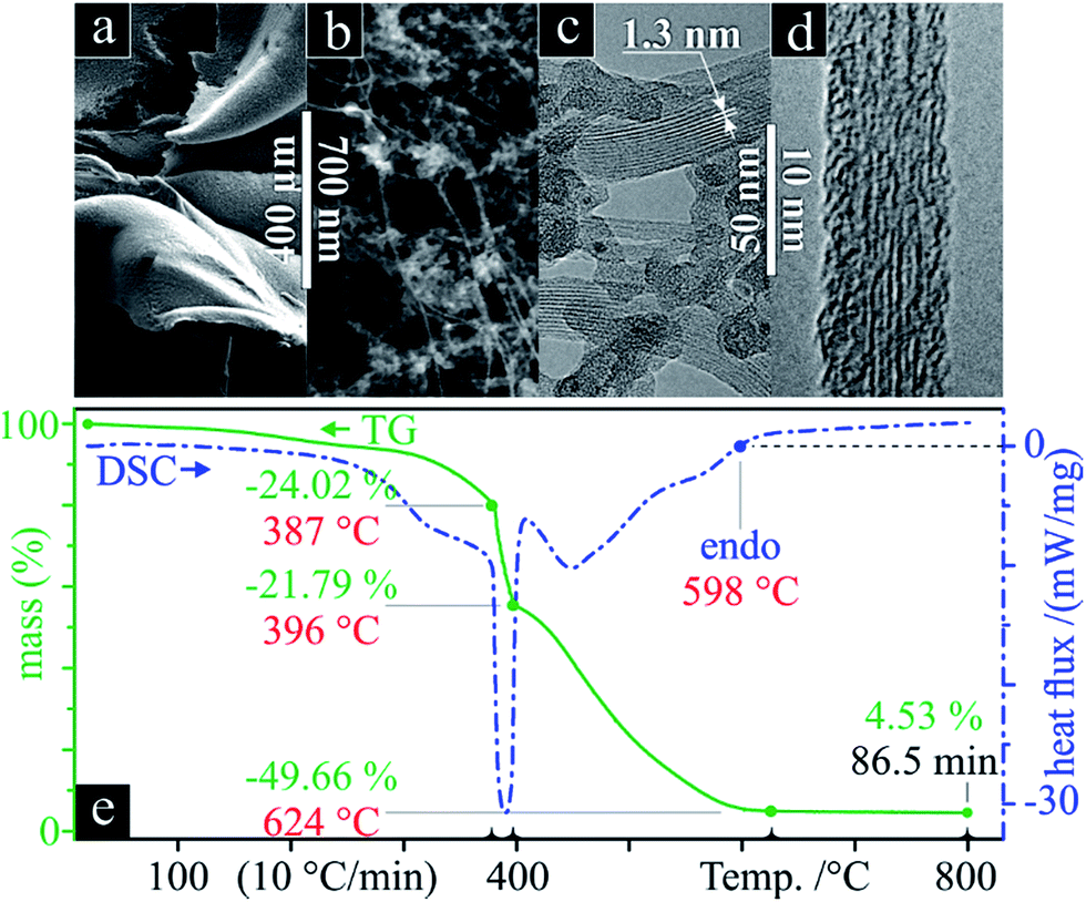 | ||
| Fig. 1 SEM (a and b), TEM (c and d), TGA and DSC (d) of the pristine SWCNTs. | ||
The measured Raman spectrum (Fig. 2a) is characteristic for SWCNTs with well-defined D and G modes, overtones and combination modes, and, at low wavenumbers, radial breathing mode (RBM) vibrations. The emergence of rather broad Raman peaks with overlapping D and G modes confirms low crystallinity, and graphitic and disordered contaminants. The D- and G-band peaks found in graphite have a much higher intrinsic linewidth compared to the extremely narrow peaks of pure SWCNTs;36 thus, the broadened peaks indicate the presence of non-CNT carbon nanoforms in the as-synthesised samples.
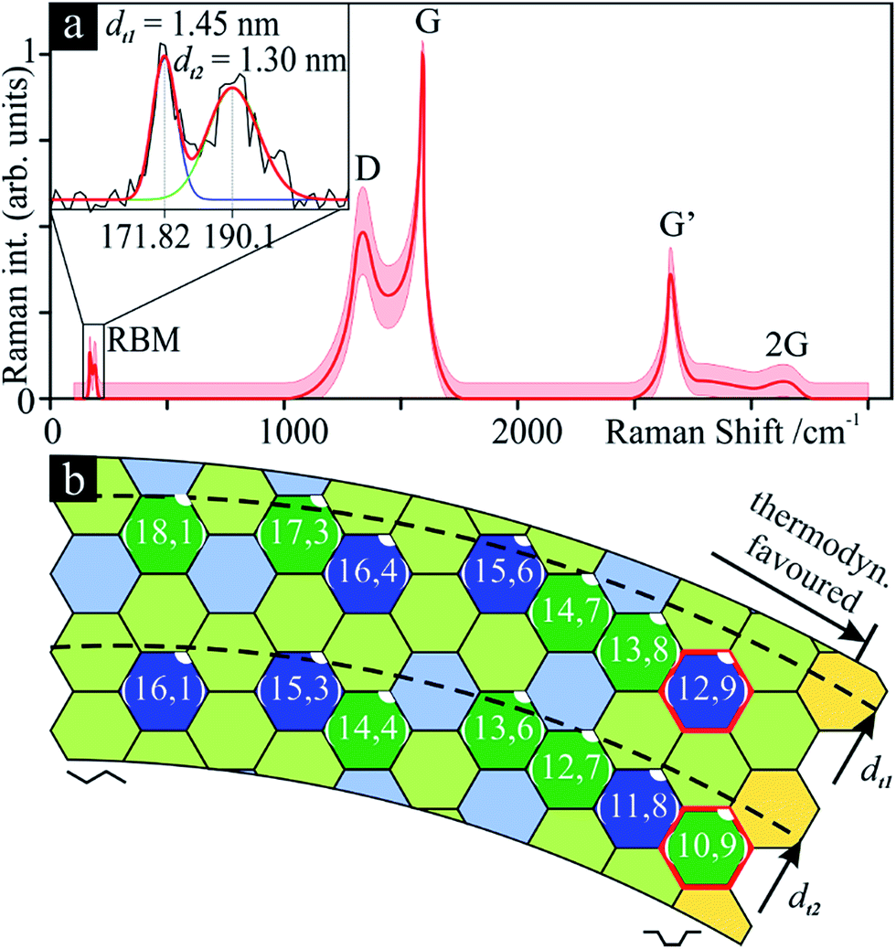 | ||
| Fig. 2 Raman spectrum averaging 10 individual scans (a) and chirality map (b) of the starting material. Light green, blue and yellow indicate semiconducting, metallic and semi-metallic tubes. The darker cells with chiral vector are the possible tubes as per RBM frequencies. The thick, red outlined cells ((10,9) & (12,9)) are near-armchair and thermodynamically favoured. | ||
The RBM arises from radial vibrations of the carbon atoms, and their frequency can be linked to the tube diameter:37
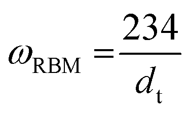
According to this, the sample contains a narrow diameter (dt) distribution with two distinct peaks indicating tube diameters of 1.45 nm (dt1) and 1.30 nm (dt2), the former slightly more intense. Considering near-armchair tubes are more thermodynamically favourable and predominantly produced,38 it is possible that the former are semiconducting (10,9) tubes and the latter are metallic (12,9) (Fig. 2b). Yet, with a spectral resolution of ca. 1.3 cm−1, these conclusions remain approximate. The initial Raman indicators for tube defects and purity are ID/IG = 0.49 and IG′/ID = 0.72, respectively.
Due to curvature effects in small-diameter tubes (e.g., SWCNTs), the G mode splits into two peaks: G− and G+. In this case, the longitudinal (tube axis) vibrations of the latter are the main contribution to this mode, versus the circumferential vibrations, which become more visible with the laser treatment. This intensity disparity and the narrow shape of G− indicates predominant semiconducting tubes,36 G+ will thus replace G in the defect ratio in this study.
The generalised ID/IG ratio is commonly used to indicate tube quality. The D mode is activated by a defect in the breathing modes of sp2-hybridised rings and its intensity is proportional to defect concentrations, but not to the actual amount of sp2 carbon39 (this only holds for an inter-defect distance above ∼2 nm;40 in our case, it remains between ca. 39 and 800 nm; calculated with ID/IG and the excitation wavelength: see Section 3.2). An sp2 lattice disturbed by sp3-bonded carbons will thus contribute to the signal, although pure sp3-hybridised carbon shows no D mode.41 The disorder-induced nature of the double-resonance D mode versus the in-plane vibrations of the graphitic structure of the G mode attests to the defect state of the tubes.42 A high-quality sample will thus approach a ratio of zero.
The second harmonic of the D mode, G′, arises from a two-phonon, second-order Raman scattering process and is insensitive to tube defects. Instead of a defect, a second phonon backscatters an electron.43 A high-quality sample produces spectra free of any signal contribution from defects with G′ intensities comparable to that of G.36 Due to this, IG′/ID is often used an indication of sample purity (i.e., absence of contaminants).42 This ratio removes conflicting chirality-dependent resonance issues and contaminant contributions that parasite the D-mode intensity (as confirmed by TGA and SEM in ref. 42), confirming and expanding on ID/IG.44
3.2. Influence of laser power
Taking the spot area, A, into account, the power density, or irradiance I, affords a comparison to previous studies and ranges between 0.04 and 44.9 kW cm−2. However, we note that the fluence, F, is actually a more meaningful expression of the energy input that the sample is submitted to; in our experiments, F is in the range of 17.2 kJ cm−2 to 17.2 MJ cm−2 and defined from the laser power, P, and exposure time, t, as follows: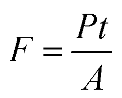
It should be noted that all Raman spectra were obtained at the non-modifying irradiance I0. The twenty-nine Raman spectra (Fig. 3) show a sharp increase in the order-induced modes (as opposed to disorder induced) RBM, G and G′ up to 13.24 kW m−2 (I1) followed by a slower decline. The disorder-induced D mode increases slightly up to ∼2.65 kW cm−2 (Ith) followed by a gradual decrease in signal strength.
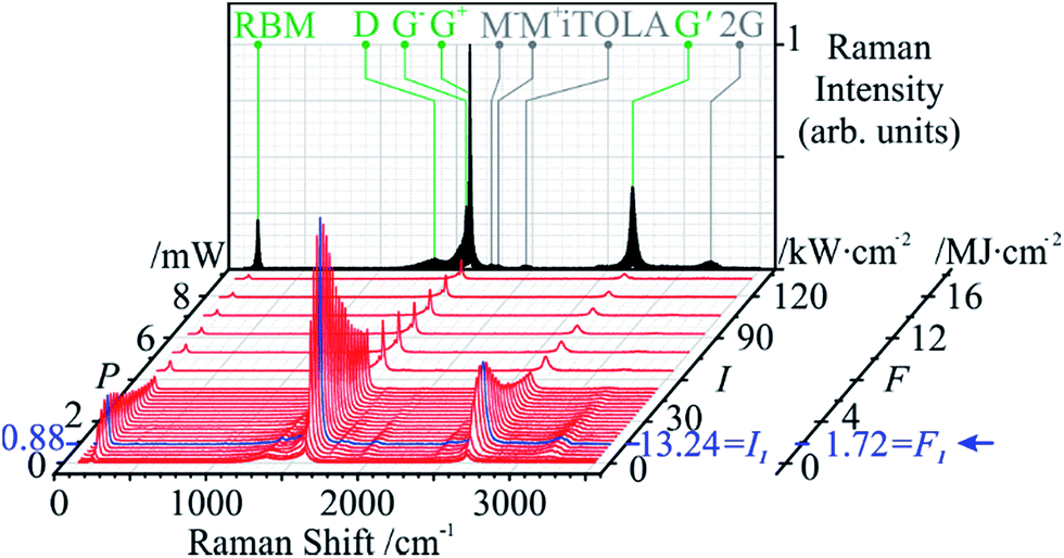 | ||
| Fig. 3 Power sweep: Raman signal vs. power (P), power density (I) and fluence (F). A sharp non-proportional increase in the intensity of the graphitic order-induced RBM, G and G′ modes is observed up to 0.88 mW (blue spectrum, marked by arrow), followed by a gradual signal intensity drop. Peaks are labelled (green & underlined, for those used in this study) on the rear plane containing the accumulated shadows of all spectra. | ||
The selected Raman modes (Fig. 4) more clearly display a strong non-proportional amplification, a maximum at I1, and a gradual decay. Apart from sample chemistry, the Raman signal strength is sensitive to concentration, aggregation state (i.e., bundling),45 excitation wavelength, and laser power. Since the two latter parameters were kept constant, the increase in Raman signal must be associated with another factor. Although laser radiation can cause bundling of tube ends in CNT forests, thus contributing to a signal increase,26 our randomly ordered samples make this rather unlikely. The effect of laser absorption by amorphous carbon to explain the initial increase of all the SWCNT features can only be limited, due to the equally intensified G′ mode. The signal decay above I1 can be attributed to material loss.
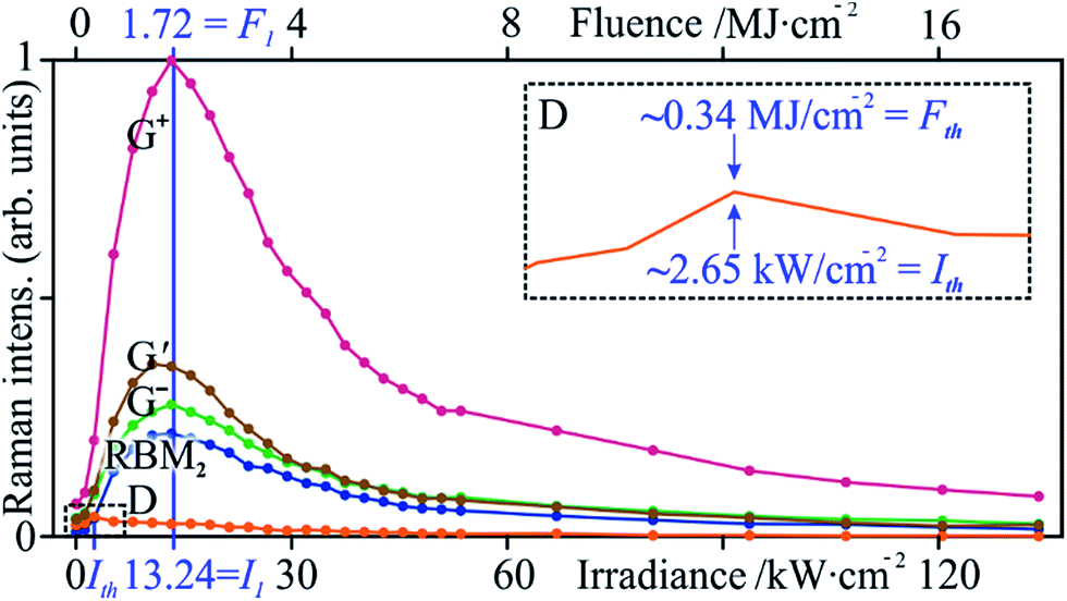 | ||
| Fig. 4 Peak intensity variations of the studied Raman modes versus laser power. All modes peak at I1 except for D, at Ith = 0.9 kW m−2. | ||
Although peak ratios are unaffected by spectrum normalisation, Fig. 4 shows important signal changes that can only be seen when not normalising the datasets to a certain value. Note that only the smaller 1.30 nm tubes (dt2) have been plotted as RBM2, since the signal of the larger 1.45 nm (dt1) tubes (RBM1) barely increases (see Fig. 8, left inset). RBM2 increases so strongly that we can eventually even see its overtone (Fig. 8, right inset).
Peak ratios and their change as a function of irradiance (Fig. 5) provide us with a more pertinent look at the state of the tubes. The irradiance Ith (maximum of ID at 2.65 kW m−2) was chosen as a threshold, below which no CNT modification is observed. It marks the onset of a sharp drop in ID/IG+, showing signs of saturation around 5.30 kW m−2 (Fig. 5a) and assuming a rather constant value at I1. Here, IG′/ID has risen to 12-fold its initial value (0.72). If indeed aromatic carbon rings and olefinic/conjugated carbon chains contribute to the G mode, these occur at lower wavenumbers than that of SWCNTs and, if detectable, would have altered the peak profile, its Lorentzian fit, and the resulting position. This was not observed, yet, their supposed contribution to G would rapidly decrease with the first curing steps, since these molecules are highly volatile under laser radiation46 and they can be incorporated in further tube growth.47 Again, to circumvent the inaccuracies that may accompany the ID/IG+ ratio, IG′/ID complements the characterisation. These two parameters, common indicators of defect and purity states, experience a 92% and 1180% improvement (at I1), respectively, with respect to the pristine material (at I0). Following this point, the defect density is stable and the purity fluctuates with a gradual downwards tendency, possibly due to tube opening. The obtained drop in defect density is similar to that of Fabbro and Da Ros,48 who utilised a CW 785 nm radiation at 573 kW m−2 in air. Their ca. 40-fold irradiance can be partly explained by a lower absorbance at said energy (1.58 eV) for both SWCNTs49 and amorphous carbon50 although their sample has different and more varied tube diameters and chiralities, which further govern absorbance.
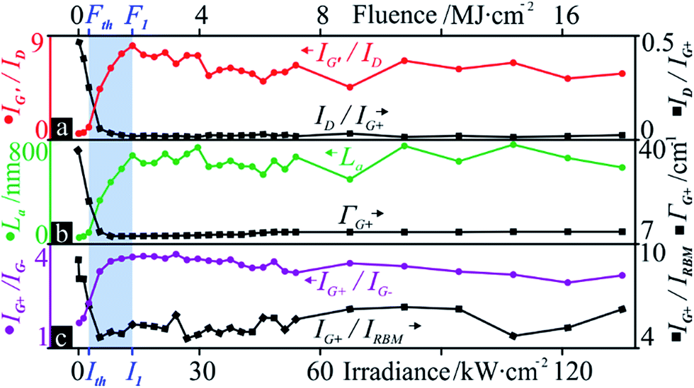 | ||
| Fig. 5 From top to bottom, all versus irradiance and fluence: Raman purity (normalized IG′/ID) and quality (ID/IG+) indicators (a); inter-defect distance (La) and full width at half maximum of G+ (ΓG+) (b); G+ vs. G− growth, i.e. G mode splitting gap (IG+/IG−), and G+ vs. RBM growth, i.e. gap between the two main order-induced peaks (IG+/IRBM2) (c). | ||
In a further analysis of tube crystallinity, the double resonance nature of the D band can be related to the mean inter-defect distance (La), derived from the coherence length in graphite,51,52 through a function of the inverse ID/IG+ ratio and the excitation wavelength λ, 532 nm in this case:
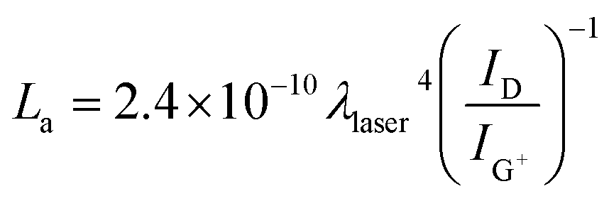
Initially intended to describe the mean in-plane crystallite size in graphite,53 the expression has since been extended to graphitic materials in general, including nanocarbons54,55 and CNTs.56
Lower defect concentrations imply a statistically greater separation between defects; thus, as the fluence increases, La saturates around I1 (Fig. 5b) with a maximum at 105 kW m−2 and almost identical fluctuations as the purity (IG′/ID). This makes sense, since G′ and G+ have a similar behaviour and, mathematically, La is an amplification of an inverse ID/IG+.
Another useful tool for the analysis of tube crystallinity is the full width at half maximum (FWHM or Γ) of a given Raman peak: a narrower vibrational band correlates with higher material crystallinity.57 However, since aromatic or benzene clusters in amorphous carbon contribute to the signal of the D mode,41 its peak narrowing would only indicate a reduction in the variety of species resonating at this frequency. An order-induced peak is more appropriate and the G mode presents the strongest signal intensity, thus reducing error. The FWHM of a deconvoluted G+ (ΓG+) shows a 70% drop and saturates around 7.9 kW cm−2 (Fig. 5b), followed by a marginal 0.9 cm−1 widening (below a local spectral resolution of 1.1 cm−1). This trend aligns well with that of the defect density and the purity.
Fig. 5c presents two peak ratios from which further conclusions can be drawn. IG+/IG− represents the G-mode splitting gap, that is, the G+-normed intensity difference between the two peeks. G-mode splitting appears in SWCNTs and although G+ is only sensitive to dt, G− depends on the tube being metallic/semiconducting36 in frequency (ω) and intensity. Metallic SWCNTs produce similar intensities for both peaks while semiconducting tubes have a very weak G− signal. In this case, IG+ went from around double IG− to almost quadrupling it at I1. Since 532 nm radiation is known to selectively burn metallic tubes,29–31 the increased G+–G− gap aligns well with metallic tubes being removed, producing a G band more closely resembling that of semiconducting tubes.36 Therefore, it is very likely that after the preferential removal of metallic tubes, predominantly semiconducting SWCNTs (the speculated (10,9) tubes with dt2 from Fig. 2) remain at I1. This is supported by the 20-fold growth of the IRBM2 vs. a mere doubled IRBM2 (Fig. 8). Although the dt2 tubes are smaller, and thus more reactive and prone to oxidation, according to Huang et al., this removal of the larger metallic tubes is related to chirality rather than size.29 This, together with the faster growth of IRBM2 vs. IG+ (Fig. 5c), points to competing mechanisms of defect removal, sample purification and loss of metallic tubes.
The strong overall increase in Raman signal strength together with the mentioned Raman indicators strongly point to an increasing level of graphitisation, defect healing, and sample purification. 130 s of 13.24 kW cm−2 (i.e., 1.72 MJ cm−2) is roughly equivalent to 10.7 × 1025 eV cm−2. At the single nanotube level, the energy input is equal to 10.7 × 10¹¹ eV nm−2 and, thus, well above the binding and migration energies for interstitials, vacancies, and other defects.10 A heat conduction model puts the surface temperature of a MWCNT film under ca. 80 mJ cm−2 of green laser light at around 800 °C.58 Above this temperature, Gorbunov and Jost argue that further growth of SWCNTs can be induced59 and we must consider that there is a huge abundance of carbon in the sample. High-temperature synthesis of SWCNTs (e.g., laser ablation) produces abundant adsorbed, reactive carbons. The ground state of carbon systems, sp2 hybridisation, remains more stable than sp3 at high temperatures,10 which promotes the growth of graphitic carbon even in amorphous carbon.60 We thus have the temperature and the carbon necessary for graphitization and tube growth. Although carbon nanotubes can coalesce,61 the absence of peak shifts in the spectra indicate no such occurrence. For the same reason, the creation of new polygonal defects can be excluded (except for Dienes or Stone–Wales defects), since these cause changes in helicity and diameter, neither of which are observed in our experiments.
The optimal irradiance seems to be I1, 13.24 kW cm−2, which when used to treat 20 different pristine sample locations with a direct exposure (no preceding step-wise increments) produces very reproducible results (Fig. 8). Interestingly, the I1 spectrum from Fig. 4 (tubes exposed with all intermediate irradiances up to and including I1) fits perfectly within this spectrum. This means that, at this exposure time (130 s), the previous energy input has no effect and tube state is solely a function of the last shot. Furthermore, repeated exposures with I1, bear no observable (Raman) effect on the tubes with equally fitting spectra.
If accumulated exposures, measured in energy or fluence, have no influence on the tube state, then the exposure time is either irrelevant or too long to observe any singularities. A study of the exposure time, well below 130 s, was thus carried out.
3.3. Influence of exposure time
At the optimal fixed irradiance of 13.24 kW cm−2 (I1), all Raman modes experienced signal amplification and eventual saturation with varying exposure times from 0.1 s to 200 s. All peak intensities saturated at 130 s (single shot if not specified otherwise), except for D, which instantly dropped to a minimum at 0.1 s (Fig. 6). Over 50% of the total changes occur within the first second of accumulated exposure.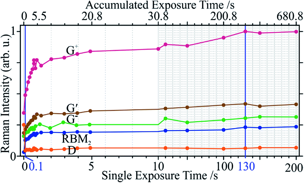 | ||
| Fig. 6 Peak intensity variations of the studied Raman modes vs. single and accumulated (nonlinear) exposure times. The D mode saturates abruptly after a 0.1 s shot, while the other modes need 130 s to do so. The time scale proportionality is stretched in the first ten seconds to show more detail. | ||
The purity does not seem to improve for an exposure longer than 1 s (Fig. 7). Carried by the stark signal decrease of the D mode, the defect density saturates at 0.1 s. Since this was the shortest (possible) exposure time, a more accurate portrayal of the sample evolution within this interval is not available. However, as with the power sweep, the defects are quickest to react to the radiation in terms of power and time. The removal of impurities requires longer times, due to the elimination of metal catalysts and metallic tubes which can leave behind open tubes. Again, a direct shot with a certain exposure time produced identical results to that of accumulated exposures of equal or lower times. This implies a build-up of slow thermal effects, necessary to remove impurities and correct defects. SWCNTs have a thermal conductivity at least 6- and 25-times that of graphite and amorphous carbon, respectively, and 10-times the thermal diffusivity.62 Hence, the temperature will rise much slower in the tubes due to more efficient energy transfer.
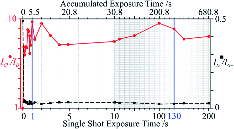 | ||
| Fig. 7 Raman defect and purity ratios vs. exposure time. The time scale proportionality of the single shot exposure is stretched in the first ten seconds to show more detail. The accumulated time axis is nonlinear. | ||
Although the purity and the defect density both saturate after ca. 1 s of exposure, peak intensities continue to increase until 130 s, possibly due to defect correction competing with metallic tube removal. The 130 s mark (t3) was thus taken as an optimal exposure time and, together with I1, were found to best heal defects and remove impurities. Direct laser curing with I1 and t3 was thus carried out on 20 different sample locations and averaged (Fig. 8). The low standard deviation attests to the reproducibility and even accommodates the corresponding spectra with previous incremental powers and times.
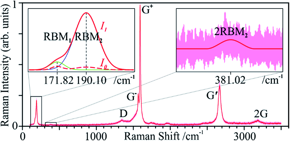 | ||
| Fig. 8 Raman spectrum after optimal irradiance I1 = 13.24 kW cm−2. The 20-location average (red) has a very low standard deviation (pink). An exposure of other sample regions with this irradiance including previous step-wise exposures produces spectra that fit within this standard deviation. Left inset: the RBM bands vs. those before the laser treatment (I0, dashed). Right inset: RBM2 is so intense that its overtone 2RBM2 is visible. R2 > 0.99. | ||
In order to explore the degree of sample modification resulting from these two parameters, in and around a produced laser spot, we performed two 20 μm (1 μm step) Raman line-scans, intersecting at the centre of said spot. The remaining parameters were identical to all other Raman measurements. ID/IG+ was calculated for each point and plotted, both scans showing Gaussian distributions in concordance with a Gaussian beam profile. Considering rotational symmetry of the beam, a 3-D surface was extrapolated from the 2-D Gauss curves resulting in a 20 × 20 μm2 grid, covering the laser spot and its surroundings (Fig. 9). The surface is slightly elliptical, due to the beam shape, which loses its symmetry in the beam path upon expansion and several reflections within the spectrometer.
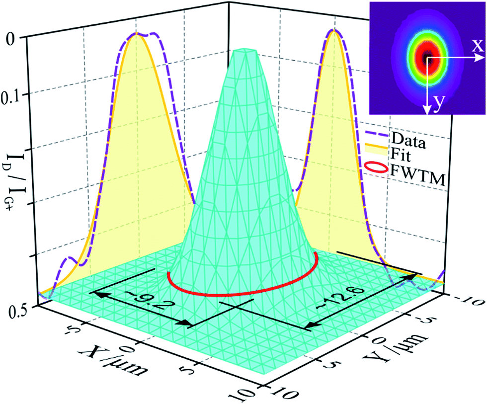 | ||
| Fig. 9 ID/IG+ over a single, irradiated spot. The asymmetric (slightly elliptic due to beam shape) 3-D Gaussian surface results from the combined parameters of two 2-D Gausses (R2 > 0.98) fitted over b-splined experimental data from intersecting Raman line maps. Note: the vertical axis is inverted to better view the 3-D surface. An average diameter of 10.9 μm (full width at tenth maximum; red ellipse) greatly exceedes the original 2.91 μm beam diameter. | ||
This plot shows very local modification to the tubes, with the best results in the centre of the spot. However, a beam diameter of ca. 3 μm results in a modification reaching ∼Ø 11 μm (full width at tenth maximum). This difference and the change of the Raman modes over time underline Hurst's findings63 in which the purification and annealing mechanisms are not limited to photochemical processes (governed by irradiance), but include photothermal effects. In agreement, we find that the CNTs are modified well beyond the beam diameter and the modification evolves over 130 s.
Each Raman spectrum was acquired directly following every laser curing step. Due to this, it is safe to assume that the sample temperature increase produced during curing had dissipated back to room temperature upon Raman excitation. This is confirmed by the absence of peak shifts in our spectra. Furthermore, a sample temperature assessment from Stokes/anti-Stokes considerations would provide that of the Raman excitation, not of the curing. In order to obtain the latter, spectra would have to be acquired during curing, excluding the possibility of varying the exposure time. Nevertheless, this was attempted and produced almost exclusively saturated spectra (even at RBM and G′ modes), hindering any data evaluation.
3.4. Laser healing and purification of mechanically damaged SWCNTs
In order to improve load transfer and electrical and thermal conduction, carbon nanotubes need to be dispersed before they can be used as fillers in composites. Agglomerates are generally broken up by a combination of sheer mixing, ultrasound, centrifugation, and sometimes aided by functionalization. As a result, in addition to the mechanical energy, collapsing cavitation bubbles produce severe heating and pressure.64 All of these techniques may thus produce defects and impurities in CNTs to various degrees.64–67 In the case of polymer matrices, defective tubes actually improve matrix/reinforcement cohesion, still enhancing the properties of the matrix. In metal matrices, the damage is critical. In either case, damage and impurities can produce excessive degradation and physical property decay. In our experiments, we subjected pristine tubes to short shear mixing and ultrasonication times.These samples present small tube bundles well below the initial 10 nm, indicating successful deagglomeration, and, as expected, damaged tubes and abundant non-CNT material (Fig. 10 “Mechanically damaged” spectrum and inset). The damaged tubes show a drastic drop in purity, IG′/ID, as a result of CNT exfoliation and the accumulation of graphitic and carbonaceous material from the mechanical damage. These damaged tubes were then laser-treated with the previously optimised parameters (I1 and t3) and characterised by Raman spectroscopy (Fig. 10 “Laser treated” spectrum and Table 1). After laser treatment, the defect density ID/IG+ drops from 0.67 to 0.04 (94%), nearly the same final value as that observed after laser annealing the pristine SWCNTs, yet a proportionately greater improvement (compared to 92%). The purity rises almost 17-fold. The recuperation is almost full, with final values similar to those of the laser-treated pristine tubes.
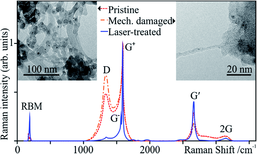 | ||
| Fig. 10 Raman spectra of the pristine, mechanically damaged and laser-treated SWCNTs. The insets show TEM micrographs of the pristine (left) and the mechanically damaged (right) samples. | ||
| Pristine | Damaged | Treated | |
|---|---|---|---|
| ID/IG+ | 0.49 ± 0.07 | 0.67 ± 0.03 | 0.04 ± 0.01 |
| IG′/ID | 0.72 ± 0.09 | 0.47 ± 0.04 | 8.56 ± 0.01 |
| ΓG+ | 35.89 ± 0.10 | 41.21 ± 0.90 | 12.01 ± 0.11 |
Table 2 puts the results presented in this study into context, with a summary of experimental conditions from the literature in which laser radiation improved the sample quality.
| Sample | VA/RO | Atm. | CW/PW | λ (nm) | I (kW cm−2) | t (s) | F (J cm−2) | Δ(ID/IG) (%) | ΔFWHM (%) | Ref. |
|---|---|---|---|---|---|---|---|---|---|---|
| a Key – vertically aligned (VA), Aka forest/randomly ordered (RO) sample; treatment atmosphere (atm.); constant wave (CW)/pulsed wave (PW) laser; laser irradiance (I); exposure time (t); laser fluence (F).b The type of nanotube was not specified. | ||||||||||
| SWCNT | RO | N2 | PW | 193 | 0.65 × 10⁻³ | 30 | — | 0 | D: −10 | 63 |
| SWCNT | RO | Air | PW | 248 | 0.45 × 10⁻³ | 30 | — | −45 | D: −24 | 63 |
| CNTb | RO | Air | PW | 248 | — | 60 × 10−9 | 0.05 | “Higher emission current” | 68 | |
| DWCNT | RO | Ar | PW | 355 | 0.016 | 13.3 | — | −9 | — | 61 |
| SWCNT | RO | Air | CW | 418 | 1.2 × 10⁻⁷ | — | — | −88 | — | 69 |
| MWCNT | RO | Air | CW | 514 | 100 | 120 × 10−9 | — | −27 | G: 0; D: −15 | 70 |
| SWCNT | RO | Air | CW | 514.5 | 25 | — | — | −77 | — | 71 |
| MWCNT | RO | Air | PW | 532 | — | 6 × 10⁻⁹ | 1 | −17 | — | 72 |
| MWCNT | RO | Air | PW | 532 | — | 5 × 10⁻⁹ | 285 | −69 | — | 58 |
| MWCNT | RO | Air | PW | 532 | — | 5 × 10⁻⁹ | 0.075 | −21 | — | 27 |
| SWCNT | RO | Air | CW | 532 | 13.24 | 130 | 17.2 × 10⁵ | −94 | G+: −71 | This study |
| SWCNT | RO | Air | CW | 632.8 | 1.0 × 10⁻⁷ | — | — | −64 | — | 69 |
| MWCNT | VA | Air | CW | 663 | 91.72 | 90 | — | −86 | — | 73 |
| SWCNT | RO | Air | CW | 785 | 573 | — | — | −94 | — | 48 |
| MWCNT | RO | Air | PW | 1064 | — | 6 × 10⁻⁹ | 0.46 | −70 | — | 58 |
| MWCNT | VA | CO2 | — | 1064 | 0.019 | — | — | “Purification” (SEM) | 74 | |
4. Conclusions
The behaviour of SWCNTs post radiation with 532 nm laser light in air has been characterised, as probed by Raman spectroscopy. Peak intensity changes, ratios, and widths have been plotted vs. a wide range of power densities and exposure times. An optimal fluence of 1.72 MJ cm−2 was determined with 0.88 mW on a 2.91 μm spot (13.24 kW cm−2) for 130 s. Although 1 s (13.24 kJ cm−2) produces similar results in terms of defects and purity, further peak intensification reveals ongoing processes up to ca. 130 s. There is evidence of thermal annealing of defects and removal of non-CNT carbonaceous species and metallic tubes. The optimised laser parameters were applied to tubes with induced mechanical damage resulting in a full recovery, compared to treated pristine tubes. The spatial characterisation of a laser-treated spot revealed a slightly elliptical Gaussian distribution of the tube modification over a surface twelve times that of the laser spot.Exposure times are often neglected in CNT irradiation studies, excluding any measure of energy input. We show that even at high power densities, the time scale of tube modification reaches 130 s, with over 50% in the first second. It should be noted that the optimal fluence for annealing and purification corresponded to a mere 5% power setting in the Raman spectrometer and a similar exposure time to that of a single-accumulation 100–3500 cm−1 scan. That is to say, CNT Raman data should be collected with previous knowledge of modification thresholds, as advised by Fabbro and Da Ros.48
The added value of this study lies in three aspects: (1) the wide-ranging and thorough variation of the power density; (2) idem for the exposure time, not considered elsewhere; and (3) the application to a real problem in the CNT community, namely, recovery of composite processing-based damage. As shown by our study, laser irradiation is an interesting and promising technique for CNT purification and defect removal, especially for surface or discrete tube treatments. Fine-tuned localised heating resulting in precision healing and purification, together with the removal of metallic or semiconducting tubes, could produce preferred electronic conduction paths in CNT films and improve existing treatments for CNT-based field effect transistors and sensors.
Acknowledgements
The authors acknowledge the EFRE Funds of the European Commission for support of activities within the AME-Lab project. This work was supported by the SUMA2 Network Project, 7th Framework Program of the European Commission (IRSES Project No. 318903), and the CREATE-Network Project, Horizon 2020 Program of the European Commission (RISE Project No. 644013). Thanks to Dr Daniel Weingarth and Dipl.-Ing. Robert Drumm (INM) for TG and DSC analyses and helpful discussions. Dr Sebastián Suárez, M.Sc. Federico Lasserre (Saarland University) and Prof. Dr Esteban Ramos Moore (Pontifical Catholic University of Chile) are kindly acknowledged for corrections and discussions. VP and MZ thank Prof. Eduard Arzt (INM) for his continuing support.Notes and references
- L. V. Radushkevich and V. M. Lukyanovich, O strukture ugleroda obrazujucegosja pri termiceskom razlozenii okisi ugleroda na zeleznom kontakte, Zurn. Fisic. Chim., 1952, 26, 88–95 CAS.
- S. Iijima, Nature, 1991, 354, 56–58 CrossRef CAS PubMed.
- N. Hamada, S. Sawada and A. Oshiyama, Phys. Rev. Lett., 1992, 68, 1579–1581 CrossRef CAS.
- J. Mintmire, B. Dunlap and C. White, Phys. Rev. Lett., 1992, 68, 631–634 CrossRef CAS.
- R. Saito, M. Fujita, G. Dresselhaus and M. Dresselhaus, Phys. Rev. B: Condens. Matter Mater. Phys., 1992, 46, 1804–1811 CrossRef CAS.
- J. A. Robinson, E. S. Snow, Ş. C. Bǎdescu, T. L. Reinecke and F. K. Perkins, Nano Lett., 2006, 6, 1747–1751 CrossRef CAS PubMed.
- M. Wong, M. Paramsothy, X. J. Xu, Y. Ren, S. Li and K. Liao, Polymer, 2003, 44, 7757–7764 CrossRef CAS PubMed.
- M. M. Shulaker, G. Hills, N. Patil, H. Wei, H.-Y. Chen, H.-S. P. Wong and S. Mitra, Nature, 2013, 501, 526–530 CrossRef CAS PubMed.
- J. Stein, B. Lenczowski, E. Anglaret and N. Fréty, Carbon, 2014, 77, 44–52 CrossRef CAS PubMed.
- P. G. Collins, in Oxford Handbook of Nanoscience and Technology: vol. 2: Materials: Structures, Properties and Characterization Techniques, ed. A. V. Narlikar and Y. Y. Fu, 2010, ch. 2 Search PubMed.
- J. Liu, A. Rinzler, H. Dai, J. Hafner, R. Bradley, P. Boul, A. Lu, T. Iverson, K. Shelimov, C. Huffman, F. Rodriguez-Macias, Y. Shon, T. Lee, D. Colbert and R. Smalley, Science, 1998, 280, 1253–1256 CrossRef CAS.
- A. V. Krasheninnikov, P. O. Lehtinen, A. S. Foster and R. M. Nieminen, Chem. Phys. Lett., 2006, 418, 132–136 CrossRef CAS PubMed.
- M. Monthioux and J. C. Charlier, Carbon, 2014, 75, 1–4 CrossRef CAS PubMed.
- Y. Piao, B. Meany, L. R. Powell, N. Valley, H. Kwon, G. C. Schatz and Y. Wang, Nat. Chem., 2013, 5, 840–845 CrossRef CAS PubMed.
- H. Jia, Y. Lian, M. O. Ishitsuka, T. Nakahodo, Y. Maeda, T. Tsuchiya, T. Wakahara and T. Akasaka, Sci. Technol. Adv. Mater., 2005, 6, 571–581 CrossRef CAS PubMed.
- S. Bandow, A. Rao and K. Williams, J. Phys. Chem. B, 1997, 5647, 8839–8842 CrossRef.
- K. B. Shelimov, R. O. Esenaliev, A. G. Rinzler, C. B. Huffman and R. E. Smalley, Chem. Phys. Lett., 1998, 282, 429–434 CrossRef CAS.
- E. Joselevich, ChemPhysChem, 2004, 5, 619–624 CrossRef CAS PubMed.
- A. Suri and K. S. Coleman, Carbon, 2011, 49, 3031–3038 CrossRef CAS PubMed.
- J. H. Warner, F. Schäffel, G. Zhong, M. H. Rümmeli, B. Büchner, J. Robertson and G. A. D. Briggs, ACS Nano, 2009, 3, 1557–1563 CrossRef CAS PubMed.
- I. V. Anoshkin, A. G. Nasibulin, P. R. Mudimela, M. He, V. Ermolov and E. I. Kauppinen, Nano Res., 2012, 6, 77–86 CrossRef.
- T. Murakami, K. Asai, Y. Yamamoto, K. Kisoda and C. Itoh, Eur. Phys. J. B, 2013, 86, 187 CrossRef.
- H. Sun, J. Wei, J. Sun, C. Ning, J. Zhu, Y. Jia, S. Yang, H. Zhu, K. Wang, D. Wu, Y. Zhao, R. Vajtai and P. M. Ajayan, RSC Adv., 2014, 4, 15502 RSC.
- K. MacKenzie, O. Dunens and A. T. Harris, Sep. Purif. Technol., 2009, 66, 209–222 CrossRef CAS PubMed.
- T. Nakamiya, T. Ueda, T. Ikegami, K. Ebihara and R. Tsuda, Curr. Appl. Phys., 2008, 8, 400–403 CrossRef PubMed.
- K. Ramadurai, C. L. Cromer, A. C. Dillon, R. L. Mahajan and J. H. Lehman, J. Appl. Phys., 2009, 105, 093106 CrossRef PubMed.
- T. Nakamiya, F. Mitsugi, K. Semba, R. Kozai, T. Ikegami, Y. Iwasaki, Y. Sonoda and R. Tsuda, Thin Solid Films, 2010, 518, 6604–6608 CrossRef CAS PubMed.
- J. R. Mialichi, M. J. S. P. Brasil, F. Iikawa, C. Veríssimo and S. A. Moshkalev, J. Appl. Phys., 2013, 114, 024904 CrossRef PubMed.
- H. Huang, R. Maruyama, K. Noda, H. Kajiura and K. Kadono, J. Phys. Chem. B, 2006, 110, 7316–7320 CrossRef CAS PubMed.
- M. Mahjouri-Samani, Y. S. Zhou, W. Xiong, Y. Gao, M. Mitchell and Y. F. Lu, Nanotechnology, 2009, 20, 495202 CrossRef CAS PubMed.
- A. Roch, T. Roch, E. R. Talens, B. Kaiser, A. Lasagni, E. Beyer, O. Jost, G. Cuniberti and A. Leson, Diamond Relat. Mater., 2014, 45, 70–75 CrossRef CAS PubMed.
- C. Thomsen and S. Reich, Light Scattering in Solids IX, 2007, vol. 232, pp. 115–232.
- S. Suarez, F. Lasserre and F. Mücklich, Mater. Sci. Eng., A, 2013, 587, 381–386 CrossRef CAS PubMed.
- T. Guo, P. Nikolaev, A. G. Rinzler, D. Tomanek, D. T. Colbert and R. E. Smalley, J. Phys. Chem., 1995, 99, 10694–10697 CrossRef CAS.
- Y. Ye, C. C. Ahn, C. Witham, B. Fultz, J. Liu, A. G. Rinzler, D. Colbert, K. A. Smith and R. E. Smalley, Appl. Phys. Lett., 1999, 74, 2307 CrossRef CAS PubMed.
- M. S. Dresselhaus, G. Dresselhaus, R. Saito and A. Jorio, Phys. Rep., 2005, 409, 47–99 CrossRef PubMed.
- C. Fantini, A. Jorio, M. Souza, M. Strano, M. Dresselhaus and M. Pimenta, Phys. Rev. Lett., 2004, 93, 147406 CrossRef CAS.
- V. Artyukhov, E. Penev and B. Yakobson, arXiv, 2014, 5, 4892.
- C. Casiraghi, A. Hartschuh, H. Qian, S. Piscanec, C. Georgi, A. Fasoli, K. S. Novoselov, D. M. Basko and A. C. Ferrari, Nano Lett., 2009, 9, 1433–1441 CrossRef CAS PubMed.
- A. C. Ferrari, Solid State Commun., 2007, 143, 47–57 CrossRef CAS PubMed.
- J. Schwan, S. Ulrich, V. Batori, H. Ehrhardt and S. R. P. Silva, J. Appl. Phys., 1996, 80, 440 CrossRef CAS PubMed.
- R. A. DiLeo, B. J. Landi and R. P. Raffaelle, J. Appl. Phys., 2007, 101, 064307 CrossRef PubMed.
- S. Reich and C. Thomsen, Philos. Trans. R. Soc., A, 2004, 362, 2271–2288 CrossRef CAS PubMed.
- R. Saito, A. Grüneis, G. G. Samsonidze, V. W. Brar, G. Dresselhaus, M. S. Dresselhaus, A. Jorio, L. G. Cançado, C. Fantini, M. A. Pimenta and A. G. Souza Filho, New J. Phys., 2003, 5, 157 CrossRef.
- A. I. López-Lorente, B. M. Simonet and M. Valcárcel, Analyst, 2014, 139, 290–298 RSC.
- U. Brand, H. Hippler, L. Lindemann and J. Troe, J. Phys., 1990, 94, 6305–6316 CAS.
- L. Pang, L. Prochazka and R. Quezada, Fuel Energy Abstr., 1995, 36, 189 Search PubMed.
- C. Fabbro and T. Da Ros, Carbon, 2014, 76, 96–104 CrossRef CAS PubMed.
- H. Kataura, Y. Kumazawa, Y. Maniwa, I. Umezu, S. Suzuki, Y. Ohtsuka and Y. Achiba, Synth. Met., 1999, 103, 2555–2558 CrossRef CAS.
- N. D. Baydoğan, Mater. Sci. Eng., B, 2004, 107, 70–77 CrossRef PubMed.
- F. Tuinstra and L. Koenig, J. Chem. Phys., 1970, 53, 1126 CrossRef CAS PubMed.
- A. C. Ferrari and J. Robertson, Phys. Rev. B: Condens. Matter Mater. Phys., 2000, 61, 14095–14107 CrossRef CAS.
- L. G. Caņado, K. Takai, T. Enoki, M. Endo, Y. A. Kim, H. Mizusaki, A. Jorio, L. N. Coelho, R. Magalhães-Paniago and M. A. Pimenta, Appl. Phys. Lett., 2006, 88, 1–4 Search PubMed.
- L. G. Cançado, A. Jorio, E. H. M. Ferreira, F. Stavale, C. A. Achete, R. B. Capaz, M. V. O. Moutinho, A. Lombardo, T. S. Kulmala and A. C. Ferrari, Nano Lett., 2011, 11, 3190–3196 CrossRef PubMed.
- M. A. Pimenta, G. Dresselhaus, M. S. Dresselhaus, L. G. Cançado, A. Jorio and R. Saito, Phys. Chem. Chem. Phys., 2007, 9, 1276–1291 RSC.
- S. Suarez, F. Lasserre, O. Prat and F. Mücklich, Phys. Status Solidi A, 2014, 211, 1555–1561 CrossRef CAS PubMed.
- L. Ian, Handbook of Raman Spectroscopy. From the Research Laboratory to the Process Line, CRC Press, New York, Basel, 2001, vol. 28 Search PubMed.
- T. Nakamiya, T. Ueda, T. Ikegami, F. Mitsugi, K. Ebihara, Y. Sonoda, Y. Iwasaki and R. Tsuda, Thin Solid Films, 2009, 517, 3854–3858 CrossRef CAS PubMed.
- R. Eason, Pulsed Laser Deposition of Thin Films, John Wiley & Sons, Inc., Hoboken, NJ, USA, 2006 Search PubMed.
- H.-J. Scheibe, D. Drescher and P. Alers, Fresenius. J. Anal. Chem., 1995, 353, 695–697 CrossRef CAS.
- Y. Zhang, T. Gong, J. Wei, W. Liu, K. Wang and D. Wu, J. Phys. Chem. C, 2007, 111, 2901–2905 CAS.
- M. Akoshima, K. Hata, D. N. Futaba, K. Mizuno, T. Baba and M. Yumura, Jpn. J. Appl. Phys., 2009, 48, 05EC07 CrossRef.
- K. Hurst and A. Dillon, J. Phys. Chem. C, 2008, 112, 16296–16300 CAS.
- H. J. Park, M. Park, J. Y. Chang and H. Lee, Nanotechnology, 2008, 19, 335702 CrossRef PubMed.
- Y. Wang, J. Wu and F. Wei, Carbon, 2003, 41, 2939–2948 CrossRef CAS.
- P. Garg, J. L. Alvarado, C. Marsh, T. A. Carlson, D. A. Kessler and K. Annamalai, Int. J. Heat Mass Transfer, 2009, 52, 5090–5101 CrossRef CAS PubMed.
- S. Song, H. Yang, R. Rao, H. Liu and A. Zhang, Catal. Commun., 2010, 11, 783–787 CrossRef CAS PubMed.
- J. Yotani, S. Uemura, T. Nagasako, H. Kurachi, H. Yamada, T. Ezaki, T. Maesoba, T. Nakao, M. Ito, T. Ishida and Y. Saito, Jpn. J. Appl. Phys., 2004, 43, L1459–L1462 CrossRef.
- P. Corio and P. Santos, Chem. Phys. Lett., 2002, 360, 557–564 CrossRef CAS.
- J. Judek, C. Jastrzebski, A. Malolepszy, M. Mazurkiewicz, L. Stobinski and M. Zdrojek, Phys. Status Solidi, 2012, 209, 313–316 CrossRef CAS PubMed.
- L. Zhang, H. Li, K.-T. Yue, S.-L. Zhang, X. Wu, J. Zi, Z. Shi and Z. Gu, Phys. Rev. B: Condens. Matter Mater. Phys., 2002, 65, 073401 CrossRef.
- T. Nakamiya, T. Ueda, T. Ikegami, F. Mitsugi, K. Ebihara and R. Tsuda, Diamond Relat. Mater., 2008, 17, 1458–1461 CrossRef CAS PubMed.
- Z. H. Lim, A. Lee, K. Y. Y. Lim, Y. Zhu and C.-H. Sow, J. Appl. Phys., 2010, 107, 064319 CrossRef PubMed.
- X. Bai, D. Li, D. Du, H. Zhang, L. Chen and J. Liang, Carbon, 2004, 42, 2125–2127 CrossRef CAS PubMed.
Footnote |
| † Electronic supplementary information (ESI) available: Beam diameter calculation, full laser irradiances and exposure times. See DOI: 10.1039/c5ra09316c |
| This journal is © The Royal Society of Chemistry 2015 |