DOI:
10.1039/C5RA09315E
(Paper)
RSC Adv., 2015,
5, 60908-60913
Enhancement of light emission in GaAs epilayers with graphene quantum dots
Received
18th May 2015
, Accepted 26th June 2015
First published on 30th June 2015
Abstract
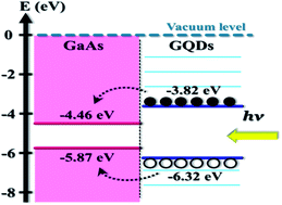
A green and one-step synthesis of graphene quantum dots (GQDs) has been implemented using pulsed laser ablation from aqueous graphene. The synthesized GQDs are able to enhance the photoluminescence (PL) of GaAs epilayers after depositing them on the GaAs surface. An enhancement of PL intensity of a factor of 2.8 has been reached at a GQD concentration of 1.12 mg ml−1. On the basis of the PL dynamics, the PL enhancement in GaAs is interpreted by the carrier transfer from GQDs to GaAs due to the work function difference between them.
1. Introduction
Graphene, which consists of a single sheet of sp2-hybridized carbon in a hexagonal structure, is a two-dimensional zero band gap material. Graphene has been exfoliated from bulk graphite by epitaxial growth, mechanical cleavage, and chemical vapor deposition.1–3 Due to its fascinating physical properties and potential applications, graphene has been studied extensively during the last decade.4–6 Graphene is capable of interacting with semiconductors as graphene is in contact with them. Recently, photoinduced electron transfer at graphene/semiconductor interfaces has gained attention.7–9 The photogenerated electrons are able to transfer from semiconductors to graphene via interfaces between them because the work function of most semiconductors is lower than that of graphene (4.7 eV).10 The electron transfer can produce a change in the electron density of semiconductors, reflecting an effect in their optical and/or electrical properties. However, such a transfer is unwanted in optical applications since the photoluminescence (PL) or photocurrent in semiconductors would be decreased after electron transfer from the semiconductors to graphene.11 It is therefore desirable to alter the electronic properties of graphene for further applications in optoelectronic devices.
Graphene quantum dots (GQDs), a class of graphene sheets with lateral dimensions less than 100 nm, reveal peculiar structural and optoelectronic properties.12–14 Unlike the absence of a band gap in graphene, GQDs produce discrete band gaps and exhibit fascinating properties such as stable PL, low toxicity, and biocompatibility. Especially, the work function of GQDs (∼3.65 eV) is lower than that of many semiconductors such as Si, GaAs, TiO2, and GaN.8,9,15,16 The electrons in this case can readily transfer from GQDs to semiconductors as the Fermi level of GQDs is higher than that of the conduction band in semiconductors. GQDs thus donate electrons into those semiconductors through the GQD/semiconductor interface and affect the optical and electrical properties of semiconductors. Accordingly, the electron transfer from GQDs to semiconductors may tailor the light emission and/or electric current in semiconductors, improving device performance in the field of optoelectronics and bio-imaging. In this work, we synthesized GQDs from aqueous graphene using pulsed laser ablation, which is a one-step, fast, and environmentally-friendly process. The synthesized products were examined by Raman spectroscopy, transmission electron microscopy (TEM), and PL, confirming the presence of GQDs. In addition, we study the effect of GQDs on the optical properties of GaAs epilayers. The PL intensity of GaAs epilayers enhances as GQDs are introduced. With an increasing concentration of GQDs, the enhancement of PL intensity in GaAs is more pronounced. According to the time-resolved PL studies, the mechanism that causes the PL enhancement in GaAs epilayers is discussed.
2. Experimental section
The GaAs epilayers studied were grown on a Si substrate by metal-organic chemical vapor deposition (MOCVD). TMGa and AsH3 were used as the sources of Ga and As, respectively. A low-temperature GaAs nucleation layer was firstly grown on the Si substrates at 450 °C. Next, a high-temperature Si-doped GaAs buffer layer with a thickness of ∼1.8 μm was grown at 650 °C and followed by the TCA (thermal cycle annealing) process. Finally, a ∼4 μm Si-doped GaAs layer was grown at 650 °C on top of the TCA buffer layer. The GQDs investigated were synthesized using the pulsed laser ablation method, which has been described elsewhere.17 The graphene for fabrication of the GQDs was purchased from Graphene Supermarket (U.S.A.). The graphene aqueous solution was placed in a quartz cell and irradiated to the pulses from an OPO laser (415 nm, 10 ns pulse, 10 Hz repetition rate) on a rotational stage (an angular velocity of 80 rpm).17 The graphene was irradiated with the laser under the fluence of 2.58 J cm−2 for 5 min. After pulsed laser ablation, the suspension product of the GQDs was filtered using a syringe filter (Millipore, 0.22 μm pore size).
The structure of the GaAs epilayers was examined by X-ray diffraction (XRD) in a θ–2θ geometry. The XRD measurements were performed using CuKα-radiation (λ = 1.541 Å) to test the phases of the samples. The microstructures of the GaAs epilayers were investigated by scanning electron microscopy (SEM) (JEOL JSM-7001F). On the other hand, the synthesized GQDs were examined by a micro Raman spectroscopy system with a laser wavelength of 532 nm as the excitation source. Transmission electron microscopy (TEM) (JEOL JEM-2100F) was used to analyze the structure of the GQDs. The composition of the GQDs was verified by X-ray photoelectron spectra (Thermo Scientific K-Alpha ESCA instrument) using a monochromatized AlKα X-ray source at 1486.6 eV. The GQDs were then deposited by drop casting a GQD solution onto the GaAs surface and dried by a heater at 50 °C. The height of the GQDs was measured by an atomic force microscopy (AFM) system (PSIA XE-100) using the tapping mode. The excitation sources in steady-state and time-resolved PL were used by CW lasers (wavelengths of 532 and 400 nm) and solid-state pulsed lasers (wavelengths of 260 and 400 nm), respectively. The collected luminescence was dispersed by a 0.75 m spectrometer and detected with a high-speed photomultiplier tube (PMT). Time-resolved PL was carried out using the technique of time-correlated single-photon counting (TCSPC). The instrument response of the time-correlated single-photon counting system is around 250 ps. The work functions of the GaAs epilayers and GQDs were measured by the Kelvin probe measurement (KP Technology, KP020).
3. Results and discussion
Fig. 1(a) shows the cross-sectional SEM micrograph of the GaAs epilayer grown on the Si substrates. The thicknesses of the GaAs epilayer and the GaAs buffer layer were found to be 3.93 and 1.81 μm, respectively. The structural properties of the GaAs epilayers were analyzed after the epitaxial growth. Fig. 1(b) shows the typical XRD 2θ–ω scan of the GaAs epilayers. A sharp reflection at 33.13° for the GaAs (002) plane was observed.18 The rocking curve of the (002) diffraction pattern from the GaAs epilayers is displayed in Fig. 1(c). The full width at half maximum (FWHM) of the rocking curve for the (002) plane is 90 arcsec, indicating a very good quality of the GaAs epilayers on the Si substrates.19
 |
| | Fig. 1 (a) The cross-sectional SEM view of the GaAs epilayers on the Si substrates. (b) The XRD pattern of the GaAs epilayer. (c) The rocking curve of the (002) diffraction peak of the GaAs epilayer. | |
Fig. 2(a) shows the TEM image of the synthesized GQDs. The diameters of the GQDs were distributed in the range of 7–12 nm, with an average of ∼8 nm. The sizes of the synthesized GQDs using pulsed laser ablation are generally consistent with those synthesized by a hydrothermal approach described in the previous report.15 The high resolution TEM (HRTEM) of a GQD is shown in Fig. 2(b), displaying a crystalline structure with an interplanar spacing of 0.212 nm, which is the (102) lattice fringes of graphene.17 To investigate the chemical structure of the GQDs, XPS measurements were carried out. Fig. 2(c) shows the C1s XPS spectrum of the GQDs. The C1s signal was deconvoluted into three peaks at binding energies of 284.4, 286.3, and 287.7 eV, corresponding to the sp2 aromatic carbon (C
C), epoxy groups (C–O), and carbonyl groups (C
O), respectively.20 Similar functional groups determined by XPS have been reported for GQDs previously.20 Fig. 2(d) displays the Raman spectrum of the as-prepared GQDs synthesized by pulsed laser ablation. The well-known D band at ∼1351 cm−1 and the G band at ∼1589 cm−1 were clearly observed, which represent the defect-induced breathing mode of the aromatic rings and the optical E2g phonons at the Brillouin zone center, respectively.17 The intensity ratio of the D and G bands is a measure of the disorder degree and is inversely proportional to the average size of the sp2 crystallite domain. The average crystallite size La can be determined according to:21,22
where
I(D) is the integrated intensity of the D band,
I(G) is the integrated intensity of the G band, and
C(
λ) is an empirical constant which depends on the wavelength of the excitation laser. According to
eqn (1), the average crystallite size
La was estimated to be 5.2 nm, comparable with the previous result in GQDs.
18 The PL of the GQDs is displayed in
Fig. 2(e), revealing a broad PL band that peaks at around 485 nm. The PL spectrum is in good agreement with those of GQDs in previous reports.
14,21 PL in GQDs has been demonstrated to be associated with the localized electron–hole pairs, oxygen-containing functional groups, and intrinsic/extrinsic states.
23–27 The PL emission peak of the synthesized GQDs shifts toward the long-wavelength region as the excitation wavelength increases (not shown). Similar broad PL spectra and excitation-dependent PL behaviors have been reported for GQDs synthesized from top-down approaches.
12 Although the GQDs can be prepared by other methods, such as hydrothermal as well as acid treatment and chemical exfoliation routes,
14,15 those methods are sometimes limited by the critical synthesis conditions (high temperatures) and time consuming. The synthesis using pulsed laser ablation in aqueous graphene is a one-step, fast, and reliable method for the preparation of GQDs.
 |
| | Fig. 2 (a) TEM image of graphene quantum dots (GQDs). (b) HRTEM image of an individual GQD. (c) XPS C1s analysis of GQDs. (d) Raman spectrum of GQDs. (e) PL spectrum of GQDs under the excitation wavelength of 260 nm. | |
The open circles in Fig. 3(a) show the PL spectrum of the GaAs epilayer without the introduction of GQDs. The PL peak wavelength is about 878 nm, assigned as the band-to-band transition in GaAs. The asymmetric shape of the PL spectrum is associated with the low defect density in the epilayers.28 The FWHM of the GaAs epilayer was determined to be 26 meV, also indicating a high quality of the GaAs epilayers on the Si substrates.28 The open squares and triangles in Fig. 3(a) show the PL spectra of the GaAs layers after incorporation of the GQDs with a concentration of 0.28 and 1.12 mg ml−1, respectively. The PL intensity from GaAs increases as the concentration of the GQDs increases. The PL intensities as a function of the GQD concentration are shown as the open squares in Fig. 3(b). The PL intensity has a maximum value at the GQD concentration of 1.12 mg ml−1, revealing an enhancement of the PL intensity by a factor of 2.3.
 |
| | Fig. 3 (a) PL spectra of the GaAs epilayers after incorporation of GQDs with different concentrations: 0 mg ml−1 (open circles), 0.28 mg ml−1 (open squares), and 1.12 mg ml−1 (open triangles). (b) The PL intensity ratio of GaAs with GQDs to untreated GaAs as a function of the GQD concentration. The carrier transfer rate as a function of the GQD concentration is also shown. | |
To find out the origin of the PL enhancement, time-resolved PL measurements were performed. The open circles in Fig. 4(a) display the PL decay profile of the bare GQDs (on a glass) monitored at a wavelength of 485 nm. The PL decay curve was fitted by the stretched exponential function:
where
n(
t) represents the carrier densities,
k represents the decay rate of carriers and
β is a dispersive exponent. The solid line in
Fig. 4(a) shows the fitted result, which is in good agreement with the experiments. In the stretched exponential function the average decay time is calculated as follows:
29| |
 | (3) |
where
Γ is the gamma function. It is known that a decrease in the PL decay time is associated with a decrease in the carrier density. If the decrease of the PL decay time in the GQDs is in parallel to the enhancement of PL in the GaAs epilayers, we can deduce that the enhanced PL intensity in GaAs comes from the carriers in the GQDs. In the absence of GaAs, the PL decay rate of the bare GQDs can be represented by
τGQD−1. Owing to the presence of an extra decay channel in GQDs, the PL decay rate of the GQDs in the hybrid case (
i.e. GQDs on GaAs) can then be described by:
| | |
τhybrid−1 = τGQD−1 + τCT−1,
| (4) |
where
τCT−1 is the rate of the carrier transfer from the GQDs to GaAs. The carrier transfer rate can thus be determined from
eqn (4) and is listed in
Table 1. The open squares and triangles in
Fig. 4 show the PL decay curves of the GQDs on top of GaAs with a concentration of 0.28 and 1.12 mg ml
−1, respectively. The PL decay transients in the GQDs on GaAs decay more pronouncedly as compared with that in the bare GQDs, indicating the presence of carrier transfer from the GQDs to GaAs. The PL decay curves in
Fig. 4(b) and (c) were also fitted by the stretched exponential function and the carrier transfer rates were determined using
eqn (2)–(4). All the fitting parameters and the obtained average decay times are listed in
Table 1. The open circles in
Fig. 3(b) show the carrier transfer rate as a function of the GQD concentration. It was found that the carrier transfer rate increases with an increasing amount of the GQD concentration. The carrier transfer rate has a maximum value at a concentration of 1.12 mg ml
−1, and then saturates after that concentration.
 |
| | Fig. 4 The PL decay profiles of the GQDs deposited on GaAs epilayers with a GQD concentration of (a) 0 (circles), (b) 0.28 (squares), and (c) 1.12 (triangles) mg ml−1. The time-resolved PL was performed under the excitation wavelength of 260 nm. The solid lines show the fitted curves using eqn (2). | |
Table 1 The dispersion components β, the decay rates k, the PL decay times of the GQDs, and the rates of the carrier transfer versus the GQD concentration
| Concentration (mg ml−1) |
β |
k (ns−1) |
〈τ〉 (ns) |
τCT−1 (ns−1) |
| 0 |
0.52 |
2.22 |
0.81 |
0 |
| 0.28 |
0.52 |
3.57 |
0.52 |
0.69 |
| 0.56 |
0.51 |
4.76 |
0.41 |
1.24 |
| 0.84 |
0.48 |
7.14 |
0.32 |
1.93 |
| 1.12 |
0.46 |
7.69 |
0.31 |
2.02 |
It is well known that the PL intensity depends on the penetration depth of the incident light, which is a measure of the sample thickness that is detected. If the thickness of the GQD layer is thicker than the penetration depth of the incident light, the effective GQD concentration would somewhat decrease, leading to an ambiguity of the PL intensity (enhancement). Therefore, it is necessary to figure out the penetration depth of the incident light and the thickness of the GQDs. The penetration depth, which is the inverse of the absorption coefficient, is not available in the literature. However, it could be found out approximately from the absorption coefficient of reduced graphene oxide and was found to be ∼500 nm for the excitation wavelength of 660 nm.30 On changing the excitation wavelength from 532 to 260 nm, the penetration length of the laser was estimated to change from ∼500 to ∼100 nm. To determine the GQD thickness, AFM measurements were performed. Fig. 5(a) and (b) show AFM images of the GQDs with a concentration of 0.28 and 1.12 mg ml−1, respectively. The average heights of the GQDs were mostly found to be ∼11 and ∼12 nm for the concentration of 0.28 and 1.12 mg ml−1, respectively (Fig. 5(c)). This indicates that the average height only increases a little for an increasing GQD concentration. Rather, the GQD density increases pronouncedly as the GQD concentration increases. The above results reveal that the GQD thickness (∼11 to 12 nm) is much thinner than the light penetration length (∼100 to 500 nm). All the carriers in the GQDs can thus be generated by photoexcitation and transfer to the GaAs epilayer for PL. The ambiguity of the PL intensity due to the partial absorption of the GQDs can thus be excluded.
 |
| | Fig. 5 AFM images of the GQDs with a concentration of (a) 0.28 mg ml−1 and (b) 1.12 mg ml−1. (c) The height profiles along the lines extracted from (a) and (b). | |
The open circles in Fig. 6(a) show the PL of the GaAs epilayer without GQDs under the excitation wavelength of 400 nm. Similar to the result in Fig. 3(a), the PL intensity from the GaAs epilayers increases as the GQD concentration increases. The PL intensities as a function of the GQD concentration are shown as the open squares in Fig. 6(b). The maximum PL intensity has an enhancement factor as high as 2.8, which is larger than that (2.3) with the excitation wavelength of 532 nm. We suggest that an excitation with the shorter wavelength (higher energy) may generate carriers with higher kinetic energy, injecting to a deeper region in the GaAs epilayer and leading to a larger PL enhancement. Fig. 6(c) shows the PL decay profiles of the GQDs without and with GQDs under the excitation wavelength of 400 nm. The open circles in Fig. 6(b) show the carrier transfer rate as a function of the GQD concentration. Similar to the result in Fig. 3(b), the carrier transfer rate increases with the GQD concentration for the excitation wavelength of 400 nm. However, the carrier transfer rate for the excitation at 400 nm is smaller than that for the excitation at 260 nm. This result may be explained by the generation of lower-energy carriers for the 400 nm excitation light, which limits the transfer of photoexcited carriers and leads to a lower carrier transfer rate.
 |
| | Fig. 6 (a) The PL decay profiles of the GQDs deposited on the GaAs epilayers with a GQD concentration of 0 (circles), 0.28 (squares), and 1.12 (triangles) mg ml−1. (b) The PL intensity ratios and carrier transfer rates as a function of the GQD concentration. (c) The time-resolved PL was performed under the excitation wavelength of 400 nm. The solid lines show the fitted curves using eqn (2). | |
To explore the mechanism of carrier transfer from the GQDs to GaAs, Kelvin probe measurements for the work function of the GQDs and GaAs were carried out. The contact potential difference (VCPD) between the sample and tip can be related to the difference in work function between them from the following equation:
| | |
eVCPD = Wtip − Wsample,
| (5) |
where
Wtip and
Wsample are the work functions of the tip and sample, respectively, and
e is the elementary charge. By measuring
VCPD, the sample work function can be estimated as long as the work function of the tip (
Wtip) is determined. Before measuring the GQD and GaAs samples,
Wtip was calibrated through a separate measurement by taking
VCPD on the Au film (with a known work function value of 5.1 eV). The subsequent
VCPD measurements determined the work function of GaAs and the GQDs to be 4.46 ± 0.02 eV and 3.82 ± 0.03 eV, respectively. The values of their work functions are comparable with the reported values in the literature.
9,15 On the basis of the Kelvin probe measurements, the carrier transfer process from the GQDs to GaAs under illumination can be interpreted by a band diagram of the GQDs and GaAs, as shown in
Fig. 7. When the GQDs are incorporated on top of the GaAs epilayers, the carriers generated by optical excitation are able to transfer from the GQDs to GaAs through the GQD/GaAs interface because the work function of the GQDs (3.82 eV) is smaller than that of GaAs (4.46 eV). The carrier transfer leads to an additional radiative recombination of carriers in the GaAs region and produces an enhancement of the PL intensity in GaAs. Due to the removal of photogenerated carriers in the GQDs, recombination of the electron–hole pairs in the GQDs would be reduced and the PL transient for the GQDs decreases accordingly. At higher concentrations of GQDs, more carriers in the GQDs can be generated by photoexcitation, leading to an increase of the carrier transfer rate and a pronounced PL enhancement in GaAs. Thus, the carriers in the GQDs are effectively transferred to GaAs, leading to a higher enhancement of PL in GaAs, as displayed in
Fig. 3(b) and
6(b).
 |
| | Fig. 7 Energy band diagram of GaAs in contact with the GQDs, describing the carrier transfer. | |
Although this study has been focused on the GaAs material, the proposed method should also be extended to other semiconductors of which the work function is larger than that of GQDs. Also, this result indicates that introducing GQDs on the semiconductor surface can be a convenient way to enhance the PL intensity in semiconductors, which promises great potential in optoelectronic devices or bio-imaging.
4. Conclusions
In summary, a one-step method for the synthesis of GQDs by pulsed laser ablation from aqueous graphene has been demonstrated. The synthesized GQDs had an average size of 8 nm, which was obtained by analysis of the TEM image. The effect of the GQDs on the enhancement of PL in GaAs epilayers has also been demonstrated. As the concentration of the GQDs increases, the PL intensity in GaAs increases accordingly. The PL intensity of GaAs has a maximum enhancement with a factor of 2.8 at a GQD concentration of 1.12 mg ml−1. We suggest that the carrier transfer owing to the work function difference between the GQDs and GaAs is responsible for the enhancement of the PL intensity in GaAs.
Acknowledgements
This project was supported in part by the Institute of Nuclear Energy Research under the grant number 1042001INER010 and the Ministry of Science and Technology in Taiwan under the grant number MOST 103-2112-M-033-004-MY3.
References
- K. S. Novoselov, A. K. Geim, S. V. Morozov, D. Jiang, Y. Zhang, S. V. Dubonos, I. V. Grigorieva and A. A. Firsov, Science, 2004, 306, 666–669 CrossRef CAS PubMed.
- C. Berger, Z. Song, X. Li, X. Wu, N. Brown, C. Naud, D. Mayou, T. Li, J. Hass, A. N. Marchenkov, E. H. Conrad, P. N. First and W. A. de Heer, Science, 2006, 312, 1191–1196 CrossRef CAS PubMed.
- K. S. Kim, Y. Zhao, H. Jang, S. Y. Lee, J. M. Kim, K. S. Kim, J. H. Ahn, P. Kim, J. Y. Choi and B. H. Hong, Nature, 2009, 457, 706–710 CrossRef CAS PubMed.
- S. Stankovich, D. A. Dikin, G. H. B. Dommett, K. M. Kohlhaas, E. J. Zimney, E. A. Stach, R. D. Piner, S. T. Nguyen and R. S. Ruoff, Nature, 2006, 442, 282–286 CrossRef CAS PubMed.
- A. K. Geim and K. S. Novoselov, Nat. Mater., 2007, 6, 183–191 CrossRef CAS PubMed.
- G. Eda, G. Fanchini and M. Chhowalla, Nat. Nanotechnol., 2008, 3, 270–274 CrossRef CAS PubMed.
- H. Ajlani, R. Othmen, M. Oueslati, A. Cavanna and A. Madouri, J. Vac. Sci. Technol., B: Microelectron. Process. Phenom., 2013, 31, 020602 Search PubMed.
- L. Wang, Y. Zhang, X. Li, E. Guo, Z. Liu, X. Yi, H. Zhu and G. Wang, RSC Adv., 2013, 3, 3359–3364 RSC.
- S. Tongay, M. Lemaitre, X. Miao, B. Gila, B. R. Appleton and A. F. Hebard, Phys. Rev. X, 2012, 2, 011002 Search PubMed.
- J. Chen, J. Shi, X. Wang, H. Cui and M. Fu, Chin. J. Catal., 2013, 34, 621–640 CrossRef CAS.
- J. Hou, C. Yang, H. Cheng, Z. Wang, S. Jiao and H. Zhu, Phys. Chem. Chem. Phys., 2013, 15, 15660–15668 RSC.
- M. A. Sk, A. Ananthanarayanan, L. Huang, K. H. Lim and P. Chen, J. Mater. Chem. C, 2014, 2, 6954–6960 RSC.
- K. J. Williams, C. A. Nelson, X. Yan, L. Li and X. Zhu, ACS Nano, 2013, 7, 1388–1394 CrossRef CAS PubMed.
- W. Chen, F. Li, C. Wu and T. Guo, Appl. Phys. Lett., 2014, 104, 063109 CrossRef PubMed.
- J. Zhao, L. Tang, J. Xiang, R. Ji, Y. Hu, J. Yuan, J. Zhao, Y. Tai and Y. Cai, RSC Adv., 2015, 5, 29222–29229 RSC.
- P. Yu, X. Wen, Y. Toh, Y. Lee, K. Huang, S. Huang, S. Shrestha, G. Conibeer and J. Tang, J. Mater. Chem. C, 2014, 2, 2894–2901 RSC.
- T. N. Lin, K. H. Chih, C. T. Yuan, C. C. Yang, J. L. Shen, C. A. J. Lin and W. R. Liu, Nanoscale, 2015, 7, 2708–2715 RSC.
- S. V. Novikov, K. W. Edmonds, A. D. Giddings, K. Y. Wang, C. R. Staddon, R. P. Campion, B. L. Gallagher and C. T. Foxon, Semicond. Sci. Technol., 2004, 19, L13–L16 CrossRef CAS.
- Y. Alaskar, S. Arafin, D. Wickramaratne, M. A. Zurbuchen, L. He, J. McKay, Q. Lin, M. S. Goorsky, R. K. Lake and K. L. Wang, Adv. Funct. Mater., 2014, 24, 6624–6638 CrossRef PubMed.
- X. Zhou, Y. Zhang, C. Wang, X. C. Wu, Y. Q. Yang, B. Zheng, H. Wu, S. Guo and J. Zhang, ACS Nano, 2012, 6, 6592–6599 CrossRef CAS PubMed.
- S. H. Song, M. Jang, J. Chung, S. H. Jin, B. H. Kim, S. Hur, S. Yoo, Y. Cho and S. Jeon, Adv. Opt. Mater., 2014, 2, 1016–1023 CrossRef CAS PubMed.
- T. Gokus, R. R. Nair, A. Bonetti, M. Böhmler, A. Lombardo, K. S. Novoselov, A. K. Geim, A. C. Ferrari and A. Hartschuh, ACS Nano, 2009, 3, 3963–3968 CrossRef CAS PubMed.
- K. P. Loh, Q. Bao, G. Eda and M. Chhowalla, Nat. Chem., 2010, 2, 1015–1024 CrossRef CAS PubMed.
- S. Zhu, J. Zhang, S. Tang, C. Qiao, L. Wang, H. Wang, X. Liu, B. Li, Y. Li, W. Yu, X. Wang, H. Sun and B. Yang, Adv. Funct. Mater., 2012, 22, 4732–4740 CrossRef CAS PubMed.
- F. Liu, M. H. Jang, H. D. Ha, J. H. Kim, Y. H. Cho and T. S. Seo, Adv. Mater., 2013, 25, 3657–3662 CrossRef CAS PubMed.
- L. Wang, S. J. Zhu, H. Y. Wang, S. N. Qu, Y. L. Zhang, J. H. Zhang, Q. D. Chen, H. L. Xu, W. Han, B. Yang and H. B. Sun, ACS Nano, 2014, 8, 2541–2547 CrossRef CAS PubMed.
- X. Wen, P. Yu, Y. Toh, X. Hao and J. Tang, Adv. Opt. Mater., 2013, 1, 173–178 CrossRef PubMed.
- C. W. Hsu, Y. F. Chen and Y. K. Su, Nanotechnology, 2012, 23, 495306 CrossRef PubMed.
- A. F. van Driel, I. S. Nikolaev, P. Vergeer, D. Vanmaekelbergh and W. L. Vos, Phys. Rev. B: Condens. Matter Mater. Phys., 2007, 75, 035329 CrossRef.
- R. Su, S. F. Lin, D. Q. Chen and G. H. Chen, J. Phys. Chem. C, 2014, 118, 12520–12525 CAS.
|
| This journal is © The Royal Society of Chemistry 2015 |
Click here to see how this site uses Cookies. View our privacy policy here.