
An ultra-broadband polarization-independent perfect absorber for the solar spectrum
Xunjun He*a,
Shitao Yana,
Guangjun Lub,
Qinfei Zhanga,
Fengmin Wua and
Jiuxing Jianga
aSchool of Applied Sciences, Harbin University of Science and Technology, No. 52 Xuefu Road, Nangang District, Harbin, Heilongjiang 150080, P. R. China. E-mail: hexunjun@hrbust.edu.cn
bBeijing Research Center, Delft University of Technology, No. A35, Qinghua East Road, Haidian District, Beijing, 100083, P. R. China
First published on 29th June 2015
Abstract
We numerically investigated an ultra-broadband, polarization-insensitive, and wide-angle metamaterial absorber for harvesting solar energy using arrays of cascading three sets of subunit cell structures with obviously different lateral sizes, while each of the subunit cell structures is composed of three pairs of metal–dielectric layers with the same lateral sizes but different dielectric constants. In this structure, the varying lateral dimensions provide multiple resonance main-bands in the composite structure, while the different dielectric constants of the dielectric layers induce multiple resonance sub-bands in the subunit cell. Simulation results show that the average absorption over the spectrum regime of 284–1524 nm is more than 92%. Moreover, the ultra-broadband response above 92% absorption can be still maintained even when θ reaches 30 degrees. The ultra-broadband absorption obtained is attributed to the synthetic effect by the excitation of all resonances in the multiple resonant stacks of 3 × 3 cascading metal–dielectric pairs. Our absorber design has high practical feasibility and appears to be very promising for solar cell and photonic detection applications.
1. Introduction
Electromagnetic metamaterials, composed of subwavelength structure cells arranged in periodic arrays, are a kind of artificially structured material with extraordinary electromagnetic properties unavailable in natural materials, such as negative refraction,1 invisible cloaking,2,3 and superlens.4 As a new branch of applications, recently, the metamaterial-based perfect absorbers have attracted considerable attention worldwide due to the potential applications including imaging, detecting, and sensing5–7 since the first perfect metamaterial absorber was first experimentally demonstrated by Landy et al.8 To date, they have been intensively investigated from microwave to optical frequencies.9,10 Unfortunately, these perfect absorbers usually work at a narrow wavelength range due to their resonance features of sub-wavelength units although they have wide incident angle and polarization independence. Such narrow bandwidth will hinder their practical applications that have bandwidth requirements, such as energy harvesting and photonic detection.11Metamaterials absorbers typically consist of a triple-layer metal–dielectric–metal structure where only the top metal layer is patterned to serve as an electric resonator, and the bottom metal layer acts as an optical mirror to eliminate the transmittance. The electric response can be obtained from excitation of the top metal layer readily coupled to an external electric field, while the magnetic response is provided by pairing the top layer with the bottom layer for an external magnetic field. Therefore, the bandwidth and amplitude of the absorption can be tuned by changing shape, size, thickness, and property of the metal structure and dielectric layer.12
Currently, efforts have been made by clustering multiple resonating structures with different sizes in a unit cell structure either vertically or horizontally to achieve a broad wavelength range for harvesting solar energy. For example, Aydin et al. demonstrated an ultra-thin plasmonic super absorber consisting of a metal–insulator–metal stack with crossed trapezoidal top arrays. Such an absorber exhibits broadband and polarization independent light absorption over the entire visible spectrum with an average measured absorption of 0.71 and simulated absorption of 0.85.10 Nielsen et al. experimentally demonstrated a periodic array of differently sized and circularly-shaped gap plasmon resonators with the average absorption of 94% in the entire visible wavelength range (400–750 nm).13 Song et al. numerically investigated a broadband absorber composed of a periodic array of multilayered truncated pyramids. This absorber obtained the absorption of about 99% from 0.28 μm to 1.5 μm for TE and TM waves at both room temperature and high temperature.14 He et al. reported a novel ultra-broadband absorber composed of a periodic array of taper metamaterial constructed by alternating subwavelength metal and dielectric layers. Under normal incidence, the measured absorption of the 2D absorber is over 90% in the spectrum range from 400 nm to 2.1 μm.15 However, the slight dimension variations of these broadband absorbers are hard to distinguish, which requires a sophisticated fabrication process and precision. In addition, the obtained bandwidths are restricted because the number of possible blended resonators is limited.
Up to now, however, almost all of the reported broadband absorptions have mainly focused on the metallic pattern, while the tuning performance of dielectric layer is fully ignored. In this paper, we present a novel design of ultra-broadband metamaterial absorber for harvesting solar energy by combining different lateral sizes and dielectric constants in a unit cell structure. Here, the unit cell of the proposed absorber is composed of a metallic ground plane and a cascade structure based on three sets of subunit cells with different lateral sizes, each of which consists of three pairs of metal–dielectric layers with the same lateral sizes but different dielectric constants, as a result, forming a 3 × 3 cascading metal–dielectric pair structure. In this structure, the obviously varying lateral dimensions provide multiple resonance main-bands in the composite structure, while the different dielectric constants of the dielectric layers induce multiple resonance sub-bands in the subunit cell. As a result, a broadband absorption obtained in this structure is the synthetic effect by the excitation of all resonances in the multiple resonant stacks. Simulation results show that the average absorption over the spectrum regime of 284–1524 nm is more than 92%. Moreover, the device can remain high absorption over a wide range of incident angles for both TE and TM waves. Therefore, the proposed ultra-broadband absorber could represent a novel candidate for future applications in solar energy harvesting and photonic detectors.
2. Designs and simulations of structures
The unit cell schematic of the proposed ultra-broadband absorber based on 3 × 3 cascading metal–dielectric pairs is shown in Fig. 1. The unit cell is composed of a metallic ground plane and a cascading structure based on three sets of subunit cells with different lateral sizes ri (i = 1, 2, 3 is the order of subunit cell), each of which consists of three pairs of metal–dielectric layers stacked along the vertical direction with the same lateral sizes but different dielectric constants εj (j = 1, 2, 3, is the order of dielectric layer in the subunit cell), represented by different colours. To simplify fabrication processes and precisions, the subunit cell structures have obviously varying lateral dimensions, and the dielectric and metal layers in the unit cell have same thickness respectively. Moreover, our structure has a square lattice with 360 degree rotational symmetry to eliminate polarization dependence of the incident light. Therefore, the structure characteristics are that the different lateral dimensions provide multiple resonance main-bands in the composite structure, while the different dielectric constants induce multiple resonance sub-bands in the subunit cell. As a result, a broadband absorption obtained in this structure is the synthetic effect by the excitation of all resonances in the multiple resonant stacks. | ||
| Fig. 1 Unit cell schematic of the proposed ultra-broadband absorber based on 3 × 3 cascaded metal–dielectric pairs. | ||
In simulation, the lateral lattice constant is chosen as P = 450 nm, which is smaller than the largest wavelength discussed here. The lateral sizes of metal circular patterns for subunit cell from the top to the bottom are r1 = 75 nm, r2 = 123 nm, r3 = 175 nm, respectively. While, the thicknesses of the dielectric, metal circular pattern and ground plane are td = 25 nm, tm = 20 nm, and tg = 200 nm, respectively. As a result, the total thickness of this device is only 605 nm (td × 9 + tm × 9 + tg). In subunit cell, moreover, MgF2, Al2O3, and SiO2 from top layer to bottom layer are chosen as the dielectric layers with their dielectric constants ε1 = 1.74 (loss tangent![[thin space (1/6-em)]](https://www.rsc.org/images/entities/char_2009.gif) 0.035), ε2 = 2.28 (loss tangent0.04), and ε3 = 3.9 (loss tangent0.025), respectively.16 Such design consists in that the resonant frequency of the structure with same lateral dimensions exhibits redshift with increasing the dielectric constant of the dielectric layer.17 Consequently, the resonant absorption at wavelengths close to each other would be excited in stacking dielectric layers with different dielectric constant and form a broadband absorption. While, the dielectric properties of metal gold used in our structure is taken from the Johnson and Christy.18
0.035), ε2 = 2.28 (loss tangent0.04), and ε3 = 3.9 (loss tangent0.025), respectively.16 Such design consists in that the resonant frequency of the structure with same lateral dimensions exhibits redshift with increasing the dielectric constant of the dielectric layer.17 Consequently, the resonant absorption at wavelengths close to each other would be excited in stacking dielectric layers with different dielectric constant and form a broadband absorption. While, the dielectric properties of metal gold used in our structure is taken from the Johnson and Christy.18
In this structure, full-wave numerical simulations of the proposed device were performed by using a finite difference time domain (FDTD) method. Periodic boundary conditions are used for a unit cell in the x and y directions, and the z plane has a perfectly matched layer boundary condition. The plane waves are normally incident to the structure along the z direction, as shown in Fig. 1. The absorption is calculated from the scattering parameters as A(λ) = 1 − R(λ) − T(λ), where R(λ) = |S11|2 represents the reflection, and T(λ) = |S21|2 represents the transmission which is zero here since the thickness of the metallic ground plane is much larger than the skin depth. As a result, the A is calculated by A = 1 − R.
3. Simulation results and discussions
To clearly explain the formation process and mechanism of the broadband absorption, two cascading structures (e.g., 3 × 1 and 3 × 2 shown in the Fig. 2(a) and (b)) are simulated. The simulated absorption spectra of the two different structure absorbers as a function of wavelengths are shown in Fig. 2. For the case of 3 × 1 cascading structure which includes three pairs of metal–dielectric layers with different lateral sizes but same dielectric constant (as shown in Fig. 2(a)), three adjacent absorption peaks appear and form a broad absorption main-band, whose bandwidth over 92% absorption is 399 nm (as shown in Fig. 2(d)). This can be attributed to the fundamental resonance modes resulted from three sets of subunit cells with different lateral sizes. In addition, there are two absorption peaks at 282 nm and 406 nm due to the hybridized coupling modes. Increasing another pair of metal–dielectric layer with the same lateral sizes but different dielectric constants in each subunit cell structure to construct 3 × 2 cascading structure (as shown in Fig. 2(b)), as shown in Fig. 2(e), more absorption peaks are observed in absorption spectrum due to the additional multiple resonant stacks. Moreover, the absorption bandwidth over 92% is broadened and become 509 nm. The phenomenon can be explained by the relationship between the absorption peak wavelength and the dielectric constant, where resonant absorption at wavelengths close to each other would be excited in stacking dielectric layers with different dielectric constants and form a broadband absorption.19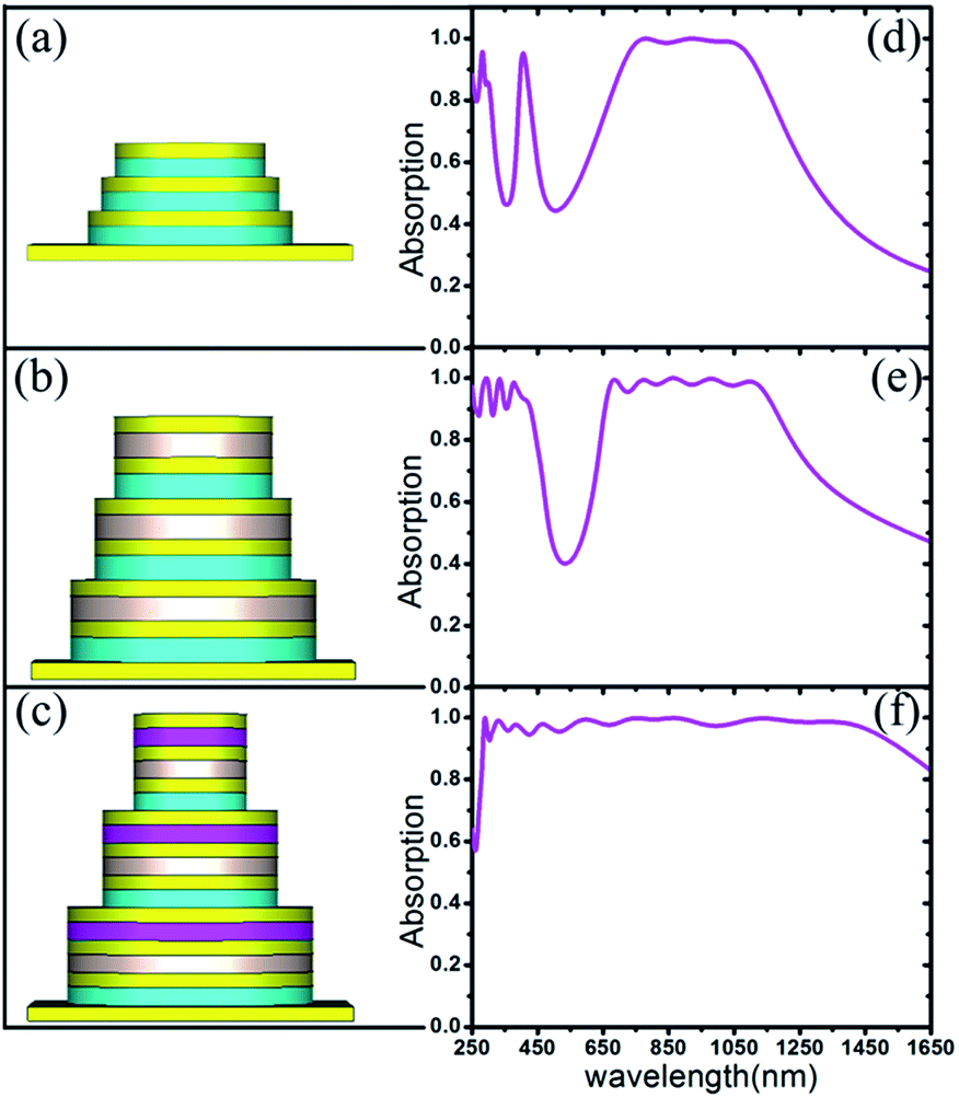 | ||
| Fig. 2 Unit cell schematics and absorption responses of different cascading structures. (a and d) 3 × 1 cascading structure, (b and e) 3 × 2 cascading structure, (c and f) 3 × 3 cascading structure. | ||
Based on above analysis, we stack three pairs of metal–dielectric layers in each subunit cell structure to further extend the absorption bandwidth (as shown in Fig. 2(c)). In this structure, high absorption of over 92% is achieved in a wide frequency range of 284–1524 nm, as shown in Fig. 2(f). The absorption bandwidth (1240 nm) of the proposed 3 × 3 absorber structure is 3.1 and 2.4 times larger than those of 3 × 1 and 3 × 2 absorber structures, respectively. Moreover, the absorption band is about 137% of the center wavelength, which is larger than that of previous reports.10,17 This explicitly implies a very good wideband absorption property. Here, this broadband absorption can be attributed to the synthetic effect of the excitation of all resonances by stacking the multiple subunit cell structures and metal–dielectric layers in each subunit cell. Therefore, an ultra-broadband absorption can be obtained by cascading multiple subunit cell structures with different lateral sizes and stacking vertically multiple metal–dielectric layers with same lateral sizes but different dielectric constants in each cascading subunit cell structure.
To better understand the mechanism of the ultra-broadband absorption characteristics, we calculated the magnetic field distributions of the proposed absorber for TE-polarized (E//x) excitation wave. The magnetic field intensities in the plane of y = 0 for different resonant wavelengths are plotted in Fig. 3. Different magnetic field distributions are observed for the wavelengths at 1363 nm, 833 nm and 500 nm, where the magnetic fields are respectively confined in the different subunit cell structures, corresponding to the fundamental magnetic responses of different lateral size structures. For instance, as incident light is a longer wavelength at λ = 1363 nm, the magnetic field distributions are strongly localized in the bottom subunit cell structure with a larger lateral size (r3 = 175 nm), and other subunit cells are very weak and completely ignored (as shown in Fig. 3(a)). For a shorter wavelength at λ = 500 nm, the magnetic fields are mainly focused on the top subunit cell structure where the circular pattern has a smaller lateral size (r1 = 75 nm), whereas there is almost no strong field concentration in the middle and bottom subunit cells (as shown in Fig. 3(c)). Moreover, these field distributions are significantly different from the previous reported results,20 where several neighboring metal and dielectric patches together support a resonant mode due to slowly varying in width of neighboring metal patches. At the same time, we also observe that the electric fields appear at corresponding complementary spatial positions (no. shown) and excite the corresponding fundamental electric responses. Therefore, both electric and magnetic resonances exist in this unit cell structure. Moreover, their resonant wavelengths are nearly positive proportional to the lateral size. In addition, we notice that the field distributions in Fig. 3(d) are strongly concentrated on the top and middle subunit cell structures, which is distinct from that of Fig. 3(a)–(c). This is attributed to the interaction of adjacent subunit cells, as a result, leading to a high-order resonance response (hybridized magnetic resonance), as shown in absorption spectra of Fig. 2.
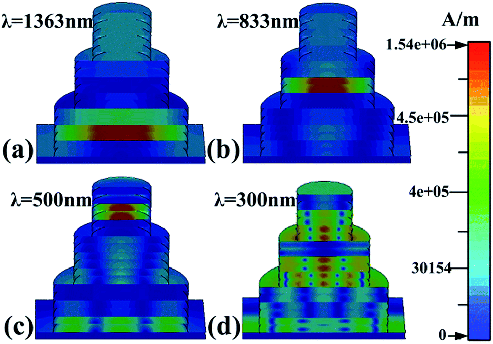 | ||
| Fig. 3 Magnetic field distributions in y = 0 plane for the different resonant wavelengths: (a) 1363 nm, (b) 833 nm, (c) 500 nm and (d) 300 nm. | ||
In this absorber, however, stacking of multiple pairs of metal–dielectric layers with different dielectric constants in subunit cell structure plays an important role for broadband absorption except for blending multiple subunit cells with different lateral sizes. This can further broaden the absorption bandwidth and form a considerable broad flat-top absorption band. To understand the broadband absorption contributions from the different dielectrics, we calculated the absorption spectrum and magnetic field distributions of single a subunit cell structure with same lateral size of r = 75 nm but the different dielectric constants, as shown in Fig. 4. As shown in Fig. 4(a), we observe that there are three adjacent absorption peaks in absorption spectrum which locate at λ1 = 588 nm, λ2 = 500 nm, and λ3 = 405 nm, respectively. Moreover, the three adjacent absorption peaks can construct a broad absorption sub-band due to closely positioned resonances compared with single a metal–dielectric layer. These absorption peaks arise from the interaction incident wave with corresponding metal–dielectric layer of different dielectric constants.
 | ||
| Fig. 4 Absorption spectrum and magnetic field distributions of single a subunit cell structure with r = 75 nm: (a) absorption spectrum simulation and (b) magnetic field distributions in y = 30 plane for different wavelengths of λ1 = 588 nm, λ2 = 500 nm, λ3 = 405 nm, and λ4 = 285 nm. | ||
To further reveal the physical origin of these absorption peaks, magnetic field distributions at three absorption peaks are presented in Fig. 4(b). Similar to the previous absorption mechanism of different lateral sizes, different field distributions are observed for three adjacent wavelengths at 588 nm, 500 nm and 405 nm. For example, for the absorption peak at 588 nm, the magnetic fields are strongly trapped in the bottom metal–dielectric layer of the subunit cell, where the SiO2 is used as dielectric layer with larger dielectric constant of 3.9. As further decreasing in wavelength (such as λ = 500 nm or 405 nm), here, the magnetic fields are mainly focused on the middle and top metal–dielectric layers where the dielectric layers are Al2O3 (ε2 = 2.28) and MgF2 (ε1 = 1.74), respectively. These results indicate that the fundamental magnetic responses of three dielectric constants are respectively excited in their respective metal–dielectric layer where the magnetic fields are totally trapped. Moreover, the fundamental magnetic resonant frequency exhibits redshift as increasing in dielectric constant, which can also observe in the previous reports.17,19 However, they are fully different from the previous broadband absorbers based on the thickness tuning of dielectric layer.21,22 In addition, we also observe that another absorption peak appears at λ4 = 285 nm. This can be attributed to the hybridized mode of the magnetic resonances, which is demonstrated by the magnetic field distributions as shown in Fig. 5(b). As a result, an ultra-broadband absorber is obtained by combining the fundamental resonances with high-order resonances of the cascading unit cell structure. Therefore, this suggests a new way to obtain an ultra-broadband absorber by stacking multiple metal–dielectric layers with different dielectric constants in a unit cell structure.
 | ||
| Fig. 5 Dependence of absorption performance on polarization and incident angle: (a) TE and TM waves and (b) different incident angles for TE wave. | ||
After the mechanism of ultra-broadband absorption has been explained, next, the polarization and angular dependences of the cascading absorber are discussed, as shown in Fig. 5. Due to the 360 degree structure symmetry of the designed absorber in x–y planes, the absorption is insensitive to TE and TM polarization light waves, as shown in Fig. 5(a). Therefore, only the TE polarization is considered in the following simulations for simplifying. Fig. 5(b) shows that the absorption effect is robust for non-normal incidence. We notice that the ultra-broadband absorption response can be maintained when θ is below 30 degrees. As further increasing the incident angle, the absorption becomes weaker, and some strong oscillations will appear in the shorter wavelength range [see the pink curve in Fig. 5(b)]. This could be explained as the fact that beyond 40°, the incident magnetic field component become gradually small, and can inefficiently excite the magnetic resonance.23 As a result, most of electromagnetic energy of incident wave is reflected back caused by the impedance mismatch. Nevertheless, the absorption still remains above 60% even when θ reaches 50 degrees. Therefore, the simulated results reveal that the designed absorber can work over a wide range of incident angle for both TE and TM waves.
At last, we investigated the underlying mechanism of the loss to understand the contributions of each part of the metamaterial absorber, as shown in Fig. 6. Fig. 6(a) shows the absorption spectra for two different loss conditions (lossy and lossfree) of the dielectric layer. Compared with the lossy dielectric, the absorption curve of the lossfree dielectric has strong oscillation at whole absorption spectrum and the average absorption is about 86% at the wavelength range from 285 nm to 1250 nm. This result indicates that the majority of energy is dissipated as the ohmic loss within the metal layers and ground plate, which is clearly different from the previously reported data where the dielectric losses are about an order of magnitude higher than the metallic ones.24 For the wavelength beyond 1250 nm, however, the absorption amplitude of the lossfree dielectric is sharply decreased, which indicates that the majority of energy is consumed by the dielectric layers. To further broaden absorption bandwidth and improve the absorption intensity of the absorber, we design and optimize the 3 × 4 cascading structure absorber, and the optimized results are presented in Fig. 6(b). Compared with the 3 × 3 cascading structure, the oscillation of absorption spectra in the shorter wave range becomes weaker and nearly vanishes as increasing in metal–dielectric layer of subunit cell structure, finally obtaining a smooth absorption spectrum.
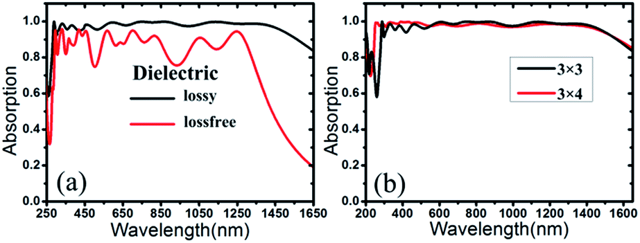 | ||
| Fig. 6 Absorption spectra for (a) different dielectric conditions (lossy and lossfree) and (b) different layer numbers of stacking structures. | ||
4. Conclusions
In conclusion, we have demonstrated an ultra-broadband metamaterial absorber for harvesting solar energy by stacking three sets of subunit cell structures with different lateral sizes and three pairs of metal–dielectric layers with the same lateral sizes but different dielectric constants in each subunit cell to merge together their fundamental and hybridized resonances. A high absorption of over 92% is achieved in a wide frequency range of 284–1524 nm in the 3 × 3 cascading structure. Moreover, the 3 × 3 cascading structure also exhibits wide incident angle and polarization insensitivity. Importantly, the design idea has high practical feasibility due to simplifying the nano-fabrication process and precision. This suggests a new way to obtain an ultra-band absorber by cascading different lateral size metal–dielectric layers with different dielectric constants in a unit cell structure, which presents a novel candidate for future applications in solar energy harvesting and photonic detections.Acknowledgements
This work was supported by the National Natural Science Foundation of China (51005001 and 51402075), Heilongjiang Province Natural Science Foundation of China (F201309), the Postdoctoral Science-Research Developmental Foundation of Heilongjiang Province (LBH-Q11082), the Youth Academic Backbone Support Plan of Heilongjiang Province Ordinary College (1253G026), Special Funds of Harbin Innovation Talents in Science and Technology Research (2014RFQXJ031) and Science Funds for the Young Innovative Talents of HUST (2011).References
- C. Caloz and T. Itoh, IEEE Microw. Wireless Compon. Lett., 2004, 14, 68 CrossRef.
- J. B. Pendry, D. Schurig and D. R. Smith, Science, 2006, 312, 1780–1782 CrossRef CAS PubMed.
- A. Alù and N. Engheta, Phys. Rev. E: Stat., Nonlinear, Soft Matter Phys., 2005, 72, 016623 CrossRef.
- N. Fang, H. Lee, C. Sun and X. Zhang, Science, 2005, 308, 534–537 CrossRef CAS PubMed.
- F. B. P. Niesler, J. K. Gansel, S. Fischbach and M. Wegener, Appl. Phys. Lett., 2012, 100, 203508 CrossRef PubMed.
- F. Alves, B. Kearney, D. Grbovic and G. Karunasiri, Opt. Express, 2012, 20, 21025–21032 CrossRef PubMed.
- F. Alves, D. Grbovic, B. Kearney, N. V. Lavrik and G. Karunasiri, Opt. Express, 2013, 21, 13256–13271 CrossRef CAS PubMed.
- N. I. Landy, S. Sajuyigbe, J. J. Mock, D. R. Smith and W. J. Padilla, Phys. Rev. Lett., 2008, 100, 207402 CrossRef CAS.
- F. Ding, Y. Cui, X. Ge, Y. Jin and S. He, Appl. Phys. Lett., 2012, 100, 103506 CrossRef PubMed.
- K. Aydin, V. E. Ferry, R. M. Briggs and H. A. Atwater, Nat. Commun., 2011, 2, 517 CrossRef PubMed.
- Y. X. Cui, Y. R. He, Y. Jin, F. Ding, L. Yang, Y. Q. Ye, S. M. Zhong, Y. Y. Lin and S. L. He, Laser Photonics Rev., 2014, 8, 495–520 CrossRef CAS PubMed.
- C. M. Watts, X. Liu and W. J. Padilla, Adv. Mater., 2012, 24, 98–120 Search PubMed.
- M. G. Nielsen, A. Pors, O. Albrektsen and S. I. Bozhevolnyi, Opt. Express, 2012, 20, 13311–13319 CrossRef PubMed.
- M. W. Song, H. L. Yu, C. G. Hu, M. B. Pu, Z. J. Zhang, J. Luo and X. G. Luo, Opt. Express, 2013, 21, 32207–32216 CrossRef CAS PubMed.
- F. Ding, Y. Jin, B. R. Li, H. Cheng, L. Mo and S. L. He, Laser Photonics Rev., 2014, 8, 946–953 CrossRef PubMed.
- E. D. Palik, Handbook of Optical Constants in Solids, Academic Press, San Diego, 1991 Search PubMed.
- Y. H. Guo, L. S. Yan, W. Pan, B. Luo and X. G. Luo, Plasmonics, 2014, 9, 951–957 CrossRef CAS.
- P. B. Johnson and R. W. Christy, Phys. Rev. B: Solid State, 1972, 6, 4370–4379 CrossRef CAS.
- N. Zhang, P. H. Zhou, S. Y. Wang, W. L. Weng, J. L. Xie and L. J. Deng, Opt. Commun., 2015, 338, 388–392 CrossRef CAS PubMed.
- Y. X. Cui, K. H. Fung, J. Xu, H. J. Ma, Y. Jin, S. He and N. X. Fang, Nano Lett., 2012, 12, 1443–1447 CrossRef CAS PubMed.
- B. X. Wang, L. L. Wang, G. Z. Wang, W. Q. Huang, X. F. Li and X. Zhai, IEEE Photonics Technol. Lett., 2014, 26, 111–114 CrossRef.
- H. Ko, D. H. Ko, Y. Cho and I. K. Han, Appl. Phys. A, 2014, 116, 857–861 CrossRef CAS.
- Y. Q. Ye, Y. Jin and S. He, J. Opt. Soc. Am. B, 2010, 27, 198–504 CrossRef.
- B. X. Wang, L. L. Wang, G. Z. Wang, W. Q. Huang, X. F. Li and X. Zhai, J. Lightwave Technol., 2014, 32, 2293–2298 CrossRef.
| This journal is © The Royal Society of Chemistry 2015 |