DOI:
10.1039/C5RA09194B
(Paper)
RSC Adv., 2015,
5, 55909-55913
Tempered glass substrate effect on the growth of polycrystalline-silicon and its applications for reliable thin-film transistors
Received
17th May 2015
, Accepted 16th June 2015
First published on 16th June 2015
Abstract
In this work, we investigated a novel mechanism of polycrystalline-silicon (poly-Si) grown on tempered glass and the stability under various bias-stress effects in the performance of poly-Si thin-film transistors (TFT) fabricated on tempered glass and compared with the poly-Si TFT on bare glass. The glass shrinkage, mask misaligned width, and thermal strain of the tempered glass were 0.01 ppm, 0.9 μm, and 26.1 MPa. The compressively tensioned bare glass showed a suppression of the crystallization rate showing a small grains, whereas the tempered glass showed high crystallization rate showing a large grains. The thermal substrate stress effect on the poly-Si TFT showed serious reliability degradation, while the poly-Si TFT on tempered glass showed stable driving characteristics on the gate and hot-carrier bias stress. The better stability is due to the smooth surface and non microcracks of poly-Si on tempered glass, which is about 1.5 nm that is much smaller than that (5 nm) of a poly-Si on bare glass.
1. Introduction
Recently, polycrystalline-Si thin-film transistors (poly-Si TFTs) have been widely used in active-matrix flat panel displays (AMFPDs) with integrated peripheral circuits on the glass substrate.1–3 Moreover, the 3-D integration of very large scale integration (VLSI) technology has been developed to increase the device density.4 However, the poly-Si TFT showed poor reliability characteristics due to its randomly formed grain boundaries and rough surface state.5,6 To solve the reliability issues, X. Zeng et al. reported that the combination of NH3 and N2O plasma passivation can improve the hot-carrier stress effect because of passivating the grain-boundary.7 J. C. Kim et al. reported that large the grain size achieved by metal-induced crystallization through a capping layer can achieve a high reliability because of its smooth interface.8 I.-S. Kang et al. showed that residual NiSi2 and extended defects in the poly-Si corners degrade the reliability.9 In addition, J. H. Park et al. showed that the substrate stress during the crystallization is also a significant factor for degrading the reliability. Unlike complementary metal–oxide-semiconductor (CMOS) desiring a strain technology for scalability beyond of 90 nm, the poly-Si should avoid the strain resulting the microcracks. The microcracks assist leakage currents including the Poole–Frenkel (P–F) emissive current and gate leakage current through gate insulator. The compacted glass substrate showed a strain-free poly-Si TFT showing a stable and uniform electrical performance in the entire area. Unfortunately, the compacting process of bare glass was performed over 45 h, which is not efficient for mass productions in the industry.10
In this paper, we realize a stress-free poly-Si TFT with using the tempered glass and confirmed that substrate stress seriously degrades device reliability. The stress-free poly-Si TFT on tempered glass showed no degradation under gate-bias stress and hot carrier stress for 104 s, while the poly-Si TFT on bare glass field effect mobility degrade about 40% and showed about 5 V of threshold voltage shift under gate-bias stress and hot carrier stress.
2. Experimental
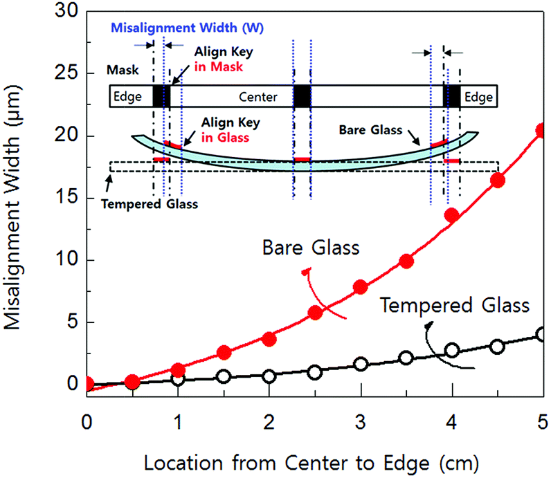
The alkaline earth boro-aluminosilicate glass, Eagle XG, was annealed at 450 °C for 12 h and cooled rapidly under N2 gaseous quenching process. The quenching process converts the bare glass to tempered glass. Then, hydrogenated amorphous silicon (a-Si:H) film was deposited by low-pressure chemical vapor deposition on the tempered glass substrate. Then the 5 nm thick of NiSi2 seeds was deposited by DC magnetron sputtering and patterned into islands. The detailed formation method of NiSi2 seeds was already reported by our group.11,12 The sample was annealed at 550 °C for 2 h in H2 ambient for crystallization. Then, 50 nm thick of Si3N4 for gate insulator was deposited and 200 nm thick of Mo0.9W0.1 alloy for gate metal was deposited. After patterning both gate metal and insulator, the source and drain were doped with B2H6 at 17 kV of accelerated voltage and 150 W of RF power. Next, the 300 nm thick of SiO2 for the inter-layer dielectric was deposited and opened for the metal contact of gate, source and drain. The poly-Si TFT on bare glass was also fabricated for the comparison. The whole fabrication process was carried out in the 1000-class clean room. Fig. 1 shows the mask misalignment width (W) of the tempered and bare glass. The W is increased from center to the edge. The bare glass showed 20 μm of W in the edges, while the tempered glass showed 3 μm of W in the edges. It can be thought that the glass has been shrunk in a compressively stress shown in the inset Fig. 1. The shrinkage rate and thermal stress of poly-Si on bare glass was 10 ppm and 200.2 MPa, whereas the shrinkage rate and thermal stress of poly-Si on tempered glass was 0.1 ppm and 26.1 MPa.
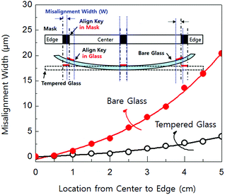 |
| | Fig. 1 Misalignment width of bare and tempered glass depending on the location. | |
3. Results and discussion
Fig. 2 shows the Raman spectra shift in poly-Si thin-films with comparing poly-Si on bare glass, poly-Si on tempered glass, and c-Si wafer. Typically, a c-Si without a considering a strain in the film shows a sharp peak at 520 cm−1 indicating that the Si atoms are in longitudinal optical (LO) phonon mode with its neighbor Si atoms. In case of strained-Si the LO-phonon peak shifts from the position of 520 cm−1 due to it stress originating from the defects or lattice mismatch between the substrate and the film from thermal annealing. However, the defects are not highly considered because, the full width at half maximum (FWHM) is smaller than 8 cm−1, and the broadening peak at 480 cm−1 indicating a transverse optical (TO) phonon mode is missing. Moreover, the stress of the poly-Si can be estimated by the Raman peak shift.12–14 The compressive stress brings a Raman spectra shift higher than 520 cm−1 while the tensile stress brings a Raman spectra shift lower than 520 cm−1. The strain can be estimated, according to the equation:12
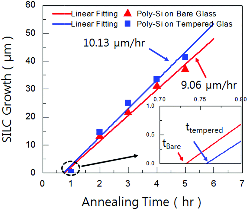
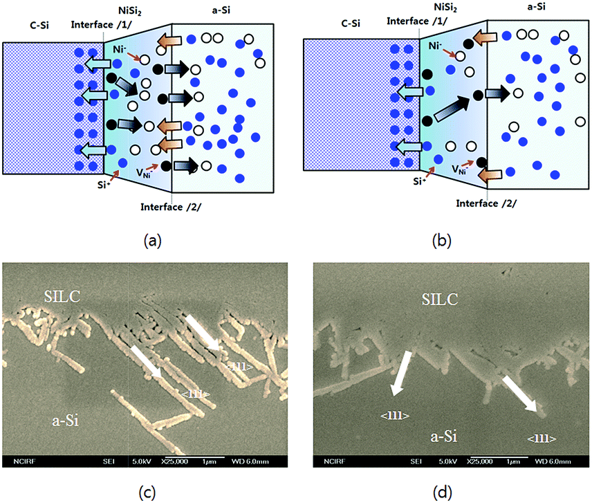
where ω is the phonon shift that is calculated from (ωs − ω0). ω0 is the wavenumber of the stress-free c-Si and ωs is the wavenumber of the film under strained poly-Si thin-film. Consequently, the strain in poly-Si on bare glass has a 340 MPa of compressive strain and the strain in poly-Si on tempered glass has about 25 MPa. In aspect of microstructure properties, the SILC poly-Si has (110) preferred texture, and (110) projected texture observed in diamond lattice structures, where the angles between two different 〈111〉 directions are either 70 or 110°. The lateral crystallization growth rate of poly-Si on bare glass and poly-Si on tempered glass wafer was shown in Fig. 3. The compressive strained growth rate was 9.10 μm h−1; while the strain-free poly-Si was 10.13 μm h−1. Previously, N.-K. Song et al. reported that the effects of the mechanical stress, during the crystallization, affect the growth behavior of MILC growth rate.15 The mechanism for this reaction is illustrated in Fig. 4(a) and (b). For the catalytic phase transformation to occur, three different atomic fluxes are required in the system. First, the bond breaking of Si–Si in a-Si and migration of each atom towards the interface between a-Si and the NiSi2 designated as F1 in Fig. 4(a). Migrated silicon atoms are to be adsorbed at the NiSi2 interface surface to create the vacancies. Second, the hopping of the vacancies inside the NiSi2 to reach the interface between the NiSi2 and poly-Si designated as F2. Hopping of vacancies should be coupled with the Ni ions in the NiSi2. Finally, the rearranging of the dissociated Si atoms in interface “/2/” was attached to the dangling bonds of poly-Si indicating F3. Phase transformation of one atomic layer can be completed by the rearrangement of dissociated silicon atoms at /2/. In a steady-state, F1 should be equal to F2 and F3.16 The external tensile stress accelerates the SILC growth rate because the strain energy along the growth direction assists the Si–Si bonding to be broken and eventually the broken Si atoms, which has a highly unstable chemical potential, is likely to be absorbed in the NiSi2/a-Si interface. Typically, the SILC growth on strain-free condition shows a needle-like structure of grains in (110) texture shown in Fig. 4(c).). On the other hand, the external compressive strain decelerates the MILC growth rate because it suppresses the breakage of Si–Si bonding by decreasing the interface energy shown in Fig. 4(b). Therefore, the MILC growth rate of compressive strain is lower than that of tensile stress with short needle-like grains shown in Fig. 4(d). Moreover, the compressively strained lateral growth showed 12 min longer incubation time than the strain-free lateral growth.
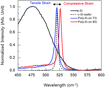 |
| | Fig. 2 Normalized Raman spectra shift characteristics of a-Si, poly-Si on tempered glass (TG), poly-Si on bare glass (BG), and c-Si wafer, respectively. | |
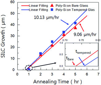 |
| | Fig. 3 SILC poly-Si crystallization growth rate on bare glass and tempered glass. | |
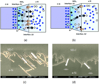 |
| | Fig. 4 Mechanism diagram of poly-Si lateral growth on (a) bare glass, and (b) tempered glass. SEM image of the poly-Si lateral growth on (c) bare glass, and (d) tempered glass. | |
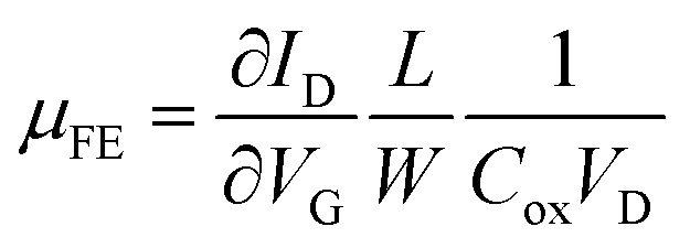
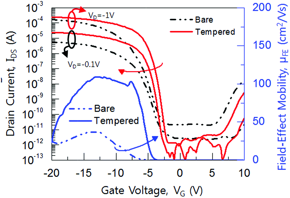
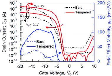
Fig. 5 shows the typical transfer curve of P-channel poly-Si TFT on bare and tempered glass and its field-effect mobility curve. The device dimension was W = L = 10 μm and the location of the device was both at the edges of the glass to see the stress effects clearly. The poly-Si TFT on bare glass exhibit a field effect mobility (μFE) of 32 cm2 V−1 s−1, a minimum leakage current (Imin,off) of <1.0 × 10⁻¹¹ A μm−1 at VD = −1 V, threshold voltage (VTH) of −6.5 V, and subthreshold slope (SS) of 0.72 V dec−1. On the other hand, the poly-Si TFT on tempered glass exhibit a μFE of 110.5 cm2 V−1 s−1, Imin,off of <1.0 × 10⁻¹² A μm−1 at VD = −1 V, VTH of −3.5 V, and SS of 0.48 V dec−1. All of the electrical properties of the poly-Si TFT on tempered glass were superior to that of poly-Si TFT on bare glass. The VTH was determined by the constant drain current method, which indicates the drain current of W/L × 10 nA at VD = −0.1 V. The μFE was extracted in the linear regime at VD = −0.1 V by the following equation:17
 |
| | Fig. 5 Transfer and field effect mobility characteristics of poly-Si TFT on bare glass and tempered glass, respectively. | |
There is a complex dependence of the μFE on gate voltage. In the low gate voltages from 0 to −7 V, the μFE is strongly influenced by both drift across the grains and thermionic emission across their grain boundaries. It can be shown that the bare glass poly-Si TFT showed dominated carrier scattering from the less dense texture. In the middle gate voltage from −7 to −15 V, the mobility shows the maximum value due to the competing the thermionic emission and interface scattering. In the high gate voltage above −15 V, it shows the carrier transports are degraded by the interface scattering.18–20
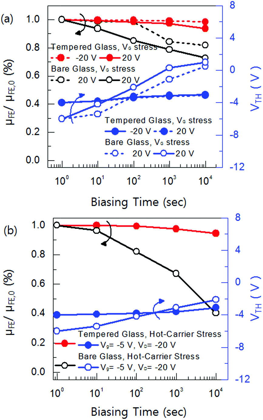
Fig. 6(a) and (b) shows the gate-bias stress at VG = 20 V and hot carrier stress at VG = −5 V and VD = −20 V, respectively. In the gate-bias stress condition, the origin of the VTH shift can be thought in two ways. One is the charge trapping into the gate insulator, which gives us a parallel shift of the transfer curve, but the charge trapping to the deep-state level degrades the SS-factor and μFE.20–24 It can be seen that the poly-Si TFT on bare glass shows about 5 V of VTH shifts after 104 s, which means the gate stress induces the electron (hole) trappings for positive (negative) gate bias into the gate insulator. In addition, the μFE mobility has been degraded more than 80% after 104 s biasing in positive and negative condition. On the other hand, the poly-Si TFT on tempered glass exhibited almost no changes in the VTH shift and μFE after 104 s. This is because neither weak bond breaking, such as Si–Si, Si–O, Si–N nor carrier trapping into the gate insulator by gate-bias stress. It indicates that the poly-Si TFT on tempered glass shows a smooth surface due to its a highly dense (111) plane, which makes a strong bonds of Si–Si, Si–O, and Si–N. In addition, the high grain boundaries and the dangling bonds at the interface, which are acting as a stepping-stone to the carriers, assist the Poole–Frenkel (P–F) emissive current. The hot-carrier stress magnificently creates the deep level traps within the gate insulator and the channel.25–27 In the results of hot carrier-stress, there was a only a little VTH shift in both poly-Si TFT on bare and tempered after 104 s. However the μFE and SS-factor of the poly-Si TFT on bare glass degraded about 60% after 104 s from the initial state, whereas there was only a little degradation in poly-Si TFT on tempered glass. It is well reported that the hot-carrier reliability in MOSFET is significantly improved by smoothing the surface, homogenous interface state, and a low defects in the near drain junctions; however the MOSFETs did not consider the substrate thermal stress due to is extremely low stress level.28–30 The thermal substrate stress can affect several factors, such as grain boundary density, microcracks, interface bonding state, and surface smoothness.
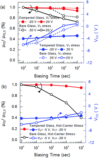 |
| | Fig. 6 Reliability of (a) negative (Vg = −20 V) and positive (Vg = 20 V) effect on the field-effect mobility variation and threshold voltage shift. (b) Hot-carrier bias stress (at Vg = −5 V, Vd = −20 V) effect on the field-effect mobility variation and the threshold voltage shift for poly-Si TFT on bare and tempered glass. | |
4. Conclusions
In this paper, we have successfully fabricated a high reliable stress-free poly-Si TFT on tempered glass and the effect was compared with the thermal stressed poly-Si TFT on bare glass. The poly-Si TFT on tempered glass exhibit a μFE of 110.5 cm2 V−1 s−1, Imin,off of <1.0 × 10⁻¹² A μm−1 at VD = −1 V, VTH of −3.5 V, and SS of 0.48 V dec−1. In addition, the gate-bias stress and hot-carrier stress showed excellent reliability. In poly-Si on tempered glass showed smoother surface roughness and a fewer microcracks than poly-Si on bare glass. Therefore, fabricating a poly-Si TFT on a stress-free substrate is an important issue for realizing the high performance device.
Acknowledgements
This work was supported in part by Eui-San Research Center and Research Institute of Advanced Materials (RIAM) both in Seoul National University, Republic of Korea. Furthermore, the work was also supported by BK21PLUS SNU Materials Division for Educating Creative Global Leaders (Grant F15SN02D1702). Thanks to Mr Gi-Sang Jung, the glass substrate, Eagle XG, was provided by Corning Precision Materials Co., Ltd. Republic of Korea.
Notes and references
- M. Stewart, et al., IEEE Trans. Electron Devices, 2001, 48, 845 CrossRef CAS.
- S.-W. Lee and S.-K. Joo, IEEE Electron Device Lett., 1996, 17, 160 CrossRef CAS.
- S. Zhang, et al., IEEE Trans. Electron Devices, 2000, 47, 569 CrossRef CAS.
- H. Yin, et al., IEEE Trans. Electron Devices, 2008, 55, 578 CrossRef CAS.
- M.-W. Ma, et al., IEEE Trans. Electron Devices, 2008, 55, 1153 CrossRef CAS.
- C. Hu, M. Wang, B. Zhang and M. Wong, IEEE Trans. Electron Devices, 2009, 56, 587 CrossRef CAS.
- X. Zeng, et al., Microelectron. Reliab., 2004, 44, 435 CrossRef CAS PubMed.
- J. C. Kim, J. H. Choi, S. S. Kim and J. Jang, IEEE Electron Device Lett., 2004, 25, 182 CrossRef CAS.
- I.-S. Kang, et al., IEEE Trans. Electron Devices, 2011, 58, 271 CrossRef CAS.
- J. H. Park, et al., IEEE Tran. Semi. Manuf., 2015, 28, 35 CrossRef.
- C. W. Byun, S. W. Son, Y. W. Lee, H. M. Kang, S. A. Park, W. C. Lim, T. Li and S. K. Joo, J. Electrochem. Soc., 2011, 158, J354 CrossRef CAS PubMed.
- C. W. Byun, S. W. Son, Y. W. Lee, H. M. Kang, S. A. Park, W. C. Lim, T. Li and S. K. Joo, J. Electrochem. Soc., 2012, 159, J115 CrossRef CAS PubMed.
- K. Kitahara, A. Moritani, A. Hara and M. Okabe, Jpn. J. Appl. Phys., 1999, 38, L1312 CrossRef CAS.
- I. D. Wolf, Semicond. Sci. Technol., 1995, 11, 139 CrossRef.
- N.-K. Song, et al., J. Electrochem. Soc., 2007, 154, H370 CrossRef CAS PubMed.
- S.-K. Joo, Electron. Mater. Lett., 2005, 1, 7 CAS.
- J. H. Park, et al., RSC Adv., 2014, 4, 47564 RSC.
- T. Chow and M. Wong, IEEE Trans. Electron Devices, 2009, 56, 1493 CrossRef CAS.
- H. N. Chern, C. L. Lee and T. F. Lei, IEEE Trans. Electron Devices, 1995, 42, 1240 CrossRef CAS.
- A. T. Hatzopoulus, D. H. Tassis, N. A. Hastas, C. A. Dimitriadis and G. Kamarinos, IEEE Trans. Electron Devices, 2005, 52, 1727 CrossRef.
- F. V. Farmkis, J. Brini, G. Kamarinos and C. A. Dimitriadis, IEEE Electron Device Lett., 2001, 22, 74 CrossRef.
- S. F. Nelson, Y.-Y. Lin, D. J. Gundlach and T. N. Jackson, Appl. Phys. Lett., 1998, 72, 1854 CrossRef CAS PubMed.
- G. Horowitz, R. Hajlaoui, D. Fichou and A. E. Kassmi, J. Appl. Phys., 1999, 85, 3202 CrossRef CAS PubMed.
- M. D. Jacunski, M. S. Shur and M. Hack, IEEE Trans. Electron Devices, 2002, 43, 1433 CrossRef.
- M. Rodder, IEEE Electron Device Lett., 1990, 11, 346 CrossRef.
- C.-F. Haung, C.-Y. Peng, Y.-J. Yang, H.-C. Sun, H.-C. Chang, P.-S. Kuo, H.-L. Chang, C.-Z. Liu and C. W. Liu, IEEE Electron Device Lett., 2008, 29, 1332 CrossRef.
- C.-F. Haung, H.-C. Sun, Y.-J. Yang, Y.-T. Chen, C.-Y. Ku, C. W. Liu, Y.-J. Hsu, C.-C. Shih and J.-S. Chen, IEEE Electron Device Lett., 2009, 30, 368 CrossRef.
- A. Acovic, G. L. Rosa and Y.-C. Sun, Microelectron. Reliab., 1996, 36, 845 CrossRef.
- H. Kufluoglu, et al., IEEE Trans. Electron Devices, 2006, 53, 1120 CrossRef CAS.
- R. P. S. Thakur, N. Chhabra and A. Ditali, Appl. Phys. Lett., 1994, 64, 3428 CrossRef CAS PubMed.
|
| This journal is © The Royal Society of Chemistry 2015 |
Click here to see how this site uses Cookies. View our privacy policy here.