Plasma functionalization and etching for enhancing metal adhesion onto polymeric substrates

C. Lambaréab, P.-Y. Tessiera, F. Poncin-Epaillard*b and D. Debarnotb
aInstitut des Matériaux Jean Rouxel, IMN, Université de Nantes, CNRS, 2 rue de la Houssinière, BP 32229, 44322 Nantes cedex 3, France
bLUNAM Université, UMR Université du Maine – CNRS n°6283, Institut des Molécules et Matériaux du Mans – Département Polymères, Colloïdes et Interfaces, Avenue Olivier Messiaen, 72085 Le Mans, France. E-mail: fabienne.poncin-epaillard@univ-lemans.fr

Received 12th May 2015 , Accepted 15th July 2015

First published on 15th July 2015


Abstract

The metallization of plastics materials, dealing with a lot of industrial applications in the field of automotive, electronic, etc.…, is generally performed by a chemical and/or electrochemical process not so ecofriendly. Therefore, this paper aims at studying an innovative two-step process for such metal coating onto ABS, ABS/PC and PEEK polymers. The first step corresponds to the plasma treatment improving the surface wettability and surface roughness. The second step is associated with the deposition of the copper metallic film by cathodic magnetron sputtering. Metallic adhesion is discussed in function of these two plasma-effects but also in function of the bias voltage or temperature substrate-holder during the film deposition. Moreover, the use of a titanium thin film as a primary layer, before copper deposition, has led to an increase of the metal/polymer adhesion.

Introduction

Metallization of polymers is essential for their applications in several domains such as microelectronic, photonic devices and medical implants in order to provide functional properties of the surface like electromagnetic shielding, wear protection, gas diffusion barrier properties or decorative purposes. However, the adhesion between metals and polymers is most of the time very poor, causing difficulties when exploring polymers metallization. Metals and polymers are rather dissimilar materials, e.g., the cohesive energy of metals is typically two orders of magnitude higher than that of polymers. One reason is that the polymer surfaces are usually nonpolar, i.e. have low surface energy. Adhesion at the metal/polymer interface is influenced by both structural and chemical properties and can be enhanced by using pre-conditioning treatments such as chemical etching,1,2 atmospheric pressure3 or low pressure plasma,4–8 ion beam6,9 as well as laser irradiation.10–13 While the former technique in liquid phase is cheap but pollutant, the latter ones take place in vapor phase with quite sophistic but ecofriendly apparatus. Plasma processes at a low pressure provide a high polymer etching and functionalization rate by a plasma chemical attack and ion sputtering effects in a synergistic manner. The plasma process modifies the polymer material and therefore, mineral particles must still adhere strongly to the polymer to provide mechanical adhesion sites for the metal layers.6 For a more efficient metallic film adhesion onto the polymeric substrate, the pre-treatment step can combine different techniques such as ion beam assisted deposition and plasma chemistry before or during the copper evaporation as for example illustrated in ref. 6. Metallization of insulating polymers is of great importance for numerous applications. The most frequently used processes for metallization are physical vapor deposition (PVD), chemical vapor deposition (CVD) and electroless metal deposition.12 PVD metal thin films deposited by argon plasma magnetron sputtering are commonly used in a very large range of industrial applications. Their main advantages are a fine control of the film thickness and a better film adhesion in comparison with evaporated thin films due to the higher energy of the sputtered metal species. Moreover, using a DC or RF substrate bias, sputtering process give the possibility to generate an Ar+ ion bombardment component before and during the thin film deposition. This Ar+ bombardment enables an increase of the surface roughness by sputtering of the polymer surface and an increase of the surface energy by creation of dangling bonds. These effects generally can lead to an improvement of the adhesion of the metal thin film. In the case of deposition on polymer substrate, a balance between the beneficial effect of the ion bombardment and the negative effect of the polymer degradation due to graphitization must be found. Recently, chemical vapor deposition of an organo–metallic precursor was also developed1 for Cu deposition onto PET. However, Jeon et al.1 show that a pre-treatment is still needed for a strong copper adhesion and the best one was, here, the almost forbidden in European countries, chromosulfuric acid pretreatment.

However, the individuality of each type of polymer regarding the effects of ion bombardment and its chemistry implies to pay attention on the fundamental mechanisms of adhesion that is based on two concepts such as the chemical adhesion including all types of chemical interactions (van der Waals, dipoles–dipoles, ionic and covalent bonds…) and the mechanical ones so-called anchoring or interlocking mechanism for which roughness is required. Plasma processes can be used to modify polymer surfaces for adhesion enhancement by introducing new reactive chemical groups and/or roughening the surfaces.14,15 The introduction of reactive chemical groups on polymer surfaces improve the wetting which results in better coating spreading to fill voids on the polymer surface for better bonding. Polymer surface roughness increases the contact areas and enhances the mechanical interlocking with the coatings, resulting in better adhesion.16 Furthermore, the self-bond strength developed over the interface of poly(ether ether ketone) (PEEK) films and evaluated by lapshear testing shows that plasma treatment of the PEEK films enhances their bonding strength, with the Ar plasma-treated films exhibiting the highest bond strength and with the nitrogen plasma the lowest.17 As illustrated in ref. 18, the adhesion between poly(oxybenzoate-co-oxynaphthoate) and deposited copper thin layer was improved by preconditioning the polymeric surface with either Ar, O2, N2 or NH3 plasmas. For all types of treatments, the hydrophilic character and the roughness of such polymer are increased; however, the adhesion between polymeric film and copper metal was mostly improved by chemical rather than physical interactions. This improvement in adhesion seems to be issued from interactions between copper metal and O[double bond, length as m-dash]C groups formed by plasma modification.

In this work, the enhancement of the adhesion strength will be discussed in function of these two parameters, functionalization yield and roughness obtained by plasma treatment for three polymers commonly used in automotive and connectic industries, the poly(acrylonitrile-butadiene-styrene) (ABS), blend of poly (acrylonitrile-butadiene-styrene) and polycarbonate (ABS/PC) and poly(ether ether ketone) (PEEK). The copper metal was deposited by magnetron sputtering of a copper target and the characteristic of the metal/polymer interface is described by pull off and scotch tests. The effect of a titanium metallic primary layer on such assembly system was also studied.

Experimental

Sample preparation

ABS (Société Sarrel), ABS/PC (Société Sarrel) and PEEK (Société Souriau) were respectively cleaned with sodium hydroxide (30 g L−1) and ethanol. Samples were immerged in solvent in ultrasonic bath during 10 min, then, rinsed with distilled water and dry on air flow.

Plasma treatment

Plasma experiments were performed in a radiofrequency plasma reactor. The discharge chamber is an aluminum rectangular chamber (volume ≅ 9 L). Two horizontal electrodes inside the chamber were driven by a 13.56 MHz generator (SAIREM) with a variable power. The incident and reflective powers were measured with power meters (METRIX). The impedance was adjusted until the reflected power was minimal. A primary pump (Adixen série Pascal 2015SD) and a turbomolecular pump (Alcatel ATP 80/100) allowed obtaining an ultimate pressure of 10−4 Pa in the reactor. The pressure was measured with a Pirani gauge (Alcatel ACC 1009) and mass flowmeters (FC 7700 CDC Area) control the amount of gas injected. In this study, three parameters were varied, the Ar gas flow (fAr, from 5 to 50 sccm), the discharge power (P, from 0 to 400 W) and the duration (t, from 0 to 45 min).

PVD metallization

The magnetron sputtering system (Alliance Concept AC 450) was composed of 2 DC magnetron sources in co-focal configuration and a RF biased rotating substrate holder. Copper (3 inches in diameter, 99.999% in purity) and titanium (3 inches in diameter, 99.999% in purity) targets were used for the thin film deposition. The distance between the targets and substrate was 130 mm. Prior to each deposition, the base pressure was lower than 6 × 10⁻⁵ Pa. The deposition pressure was fixed to 0.5 Pa for all the conditions.

The DC power applied to the copper or titanium target was fixed at 200 W. The deposition time was 10 min. In this deposition condition, the copper film thickness measured by profilometry was 400 nm. In some experiments, the substrate holder was heated from T = 30 to 100 °C and RF biased with a self-bias varying from 0 to −300 V.

For all experiments, the substrate holder was rotated at 5 rpm in order to homogenize the deposition.

Sample characterization

Wettability. Contact angles measurements ultrapure water and diiodomethane (3 μL and 1.5 μL respectively) droplets were performed using a Ramé Hart Inc. goniometer. At least, three drops of each liquid was deposited for each sample surface and each parameter studied. In order to evaluate the wettability of surfaces, the surface energy was calculated using the Owens–Wendt method with the followed equations:
image file: c5ra08844e-t1.tif

γS = γPS + γDS
XPS analyses. The XPS analyses were performed on a photo electron X spectrometer Axis Nova (Kratos Analytical). The X-ray source is a mono chromatic Al Kα. A pass energy of 20 eV was employed for high-resolution spectrum. The number of scans was 10 for the high-resolution spectrum of main XPS peak (C 1s, O 1s, N 1s, F 1s and Al 2p). The neutralizer was used for all measurement because of the non conductive substrate. The calibration was done with the main component of the C 1s peak, which was assigned to a value of 284.6 eV. The peak fitting was performed using Casa XPS software. The peak shape was chosen as Gaussian/Lorentzian area. The full width at half-maximum (FWHM) was found constant after peak fitting for each XPS peak and all studied samples.
SEM analysis. The layers were characterized by Scanning Electron Microscopy (SEM, JEOL JSM-6510 LV). The polymer surfaces were covered by a very thin sputtered layer of gold before imaging.
Thickness measurement. This measurement was performed on a profilometer Dektak 8 (Veeco) with a diamond tip.
Roughness measurement. Measurements were run with the atomic force microscope (Innova Bruker) on an analyzed area of 10 × 10 μm2 with a frequency of 1 Hz. Tips used are in Si model TESPA (Bruker) with a resonance frequency between 320 and 364 Hz and a rigidity between 20 and 80 N m−1.
Adhesion – scotch test. A cross-cut test was used to measure the adhesion of the copper layer. A grid (25 squares in 1 × 1 mm2) was drawing on the surface with a comb, according to the ISO 2409 norm.19 An adhesive was layered with a standard pressure and then removes quickly. The peeled-off surfaces were then analyzed by image treatment with Image J 1.45 software. The results were calculated as a percentage of unsticking metal.
Adhesion – pull off test. A pull off test allowed measuring the delamination strength of thin metallic film (ISO 4624 norm).20 The system was set up on the LRX Lloyd pull machine with 1000 N sensor. The traction test was applied with a speed of 1 mm min−1 and with a pre-charge of 0.001 N. Acquisition was treated with Nexygen NT Software. Tests were repeated at least three times for each parameter. The plot was pasted on the metallic surface with Araldite glue (grade 2011). The typical response of the pull test was divided in three parts. The first one corresponded to a slow increase of the strength related to the traction application. The second part with an important increasing of the strength with lengthening corresponded to the plastic area. The last part was the break of the interface polymer/metal (Cu: at ≈0.83 mm) followed by a brutal decreasing of the strength.

The adhesion was characterized by the breaking stress of the interface copper/polymer (breaking strength divided by the section, 38.48 mm2), but also the unsticking percentage determined by image treatment of the polymer surface after the mechanical test.

Results and discussion

The three polymers were plasma-treated in different atmospheres (Ar, O2, N2, Ar + O2, Ar + N2) in various plasma conditions (mixture ratio from 1/3 to 3/1, PAr = 0.2–1 Pa, P = 20–100 W, t = 0.5–5 min). Then, one set of plasma parameters was selected in function of the water contact angle since if its value depends on the functionalization, it is also altered by topographic feature. Higher, the wettability should be; lower should be the contact angle. The preliminary experiences gave evidence that in all cases, one of the best treatment is obtained with an argon plasma (P = 60 W, PAr = 0.2 Pa, t = 2 min) and the corresponding values of the water contact is reported in Table 1.
Table 1 Polymer wettability after the plasma setting (water contact angle, °), (P = 60 W, PAr = 0.2 Pa, p = 2 × 10⁻³ mbar, t = 2 min)
Polymer Pristine Treated
θH2O θH2O
ABS 91.8 ± 0.8 4.0 ± 0.0
ABS/PC 106.8 ± 2.6 3.8 ± 0.4
PEEK 79.8 ± 2.0 3.0 ± 1.4


These results show a strong decrease of the water contact angle after the plasma-treatment for all types of polymers with a threshold value of around 3.5° while those of diiodomethane probe, not shown here, are lowered (blank: θdiiodomethane ≈ 35° and plasma-treated: θdiiodomethane plasma ≈ 24°). These plasma-treated surfaces are completely wetted with water leading to the conclusion of the hydrophilic groups attachment with a high yield.

For N2 or O2 plasma-treatments, the water contact angle was decreased respectively to 5° and 8°. The Ar adduct to the N2 or O2 plasma phases little varied the wettability depending on its concentration (θH2O ≈ 8°). According to these measurements, this showed that whatever the plasma-treatment, the hydrophilic properties of polymer surfaces was always increased. The calculation of the free surface energy and its polar component also clearly indicated an increase (of around 1.6 factor) whatever the chemical nature of the plasma phase. Even if the surface modification occurs with different mechanisms depending on the plasma composition, since the closed obtained results of wettability, the study will be focused on Ar plasma-treatment because of its sputtering and etching behaviour in favour of roughness control.

Study of the balance between the chemical and interlocking adhesions of plasma-treated polymers

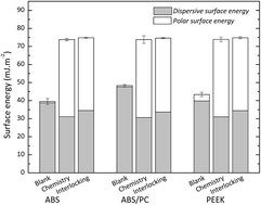
Furthermore, the comparison of the resulting surface energies in the previous conditions, so-called chemistry conditions (Fig. 1) leads to a similar conclusion, i.e. almost the same value of surface energy after the plasma-treatment, whatever the chemical nature of the polymer (around 74 mJ m−2) and its initial value associated to a huge increase of the polar component. The increase of the polar character is induced by pending radical formation on polymer surface by energetic plasma reactive species striking the surface during the plasma-treatment followed by a post-oxydation at ambient air after the plasma treatment. Indeed, the value of the energies associated to argon species striking the polymer surface Ar+ ion kinetic energy estimated to 20 eV and the Ar metastable species energy at 11.5 eV are higher enough for any polymer bond scission (EC–C = 3.6 eV; EC[double bond, length as m-dash]C = 6.4 eV; EC–H = 4.3 eV and EC[double bond, length as m-dash]O = 7.8 eV).21 Later one, the formed radicals may recombine themselves, with oxygen or nitrogen traces included in the plasma or at the atmospheric pressure leading to the polar functionalization.22–24 Further evidence of the polar groups attachment is given below in the XPS characterization.
image file: c5ra08844e-f1.tif
Fig. 1 Surface energy for polymers treated in plasma-functionalization (P = 60 W, t = 2 min, PAr = 0.2 Pa) or plasma-etching (P = 400 W, t = 45 min, PAr = 0.2 Pa) conditions.

The adhesion of thin metallic layer is dependent on the surface chemistry, i.e. the affinity of the substrate towards the metal, but also on the roughness which allows a mechanical anchoring of the deposited metal. After such a functionalizing plasma-treatment, SEM images (Table 2) did not reveal significant change of the surface topography. This result is confirmed by AFM surface analyses for which the mean square roughness (Rq) measured from 10 × 10 μm AFM images, not shown here, is invariant around 30 nm, 30 nm and 150 nm, respectively for ABS, ABS/PC and PEEK. However, SEM images of ABS/PC surfaces after exposure to an Ar ion beam showed that PC was not affected by the Ar ion beam treatment at lower times while ABS formed nanostructures.25 On the other hand, at higher treatment times, both PC and ABS are affected by the Ar+ beam and formed nanostructures.25

Table 2 SEM images (bar symbol corresponds to 5 μm) of pristine plasma functionalized (P = 60 W, PAr = 0.2 Pa, t = 2 min) and plasma etched (400 W, PAr = 0.2 Pa, t = 45 min.) polymer surfaces

image file: c5ra08844e-u1.tif

Pristine Plasma-functionalized Plasma-etched
ABS image file: c5ra08844e-u2.tif image file: c5ra08844e-u3.tif image file: c5ra08844e-u4.tif
ABS/PC image file: c5ra08844e-u5.tif image file: c5ra08844e-u6.tif image file: c5ra08844e-u7.tif
PEEK image file: c5ra08844e-u8.tif image file: c5ra08844e-u9.tif image file: c5ra08844e-u10.tif


Depending on the plasma and interface chemistries, the surface roughness and therefore the mechanical anchoring could be enhanced. In order of such an effect, degradation and etching process should be emphasized. For any physical etching, argon plasma was recommended because of its sputtering yield due to heavy and energetic ions. Higher their densities are, bigger the polymeric degradation yield is. Moreover, the argon metastable species could induce scission of the polymer chains and this effect could lead to an increase of the sputtering yield. Increasing the discharge power or the treatment duration should be in favor of the roughness appearance and the polymeric chain ablation.26–29 Moreover, the etching process is more pronounced in amorphous polymers (ABS, ABS/PC) rather than in semi-crystalline ones (PEEK).30 Therefore, such a study was only run on these former polymers.

Varying the discharge power (Fig. 2, upper) leads to a significant increase of the roughness Rq which almost doubles for discharge power of 400 W whatever the chemical nature of the polymeric substrate. One may conclude that the etching should mostly take place on the ABS phase, and more probably on the weaker component, the butadiene as already described for any type of degradation. The degradation yield, even if increasing by a factor of 6–12, differs from both polymers when studying the treatment duration influence (Fig. 2, lower). Indeed, a linear dependence is observed for the ABS while a strong and fast increase of the ABS/PC roughness is observed for duration longer than 30 min. As described in the literature,31 PC seems to be more plasma-degradable than ABS because of its photo-degradation property under UV irradiation.


image file: c5ra08844e-f2.tif
Fig. 2 Roughness dependence on drastic Ar plasma conditions (PAr = 0.2 Pa).

The surface topography of polymers treated in such optimized conditions (P = 400 W and t = 45 min) is shown in Table 2 (“plasma-etched” column). The increase of their roughness leads to the formation of dots whose diameter is around 350 nm as observed in ref. 31 and 32.

The surface energies of these plasma-etched polymeric samples are compared to that one's of substrates plasma-treated for the highest functionalization effect (Fig. 1, “interlocking” bars). Whatever the intended effect (functionalization or roughness) on these materials, the polar component of the surface energy is increasing to a maximum value of 40 mJ m−2. Therefore, one can conclude that the last series of plasma-treatment dealing the topography does not alter the surface functionalization and polarity. Even more, as the roughness is known to increase the wettability of a hydrophilic polymer because of a higher surface contact between the liquid droplet and the material,33 this type of treatment reinforces the wettability of these samples.

The XPS analysis shows that the plasma-modified surfaces are almost composed of carbon and oxygen whatever the plasma parameters selected. Depending on these parameters, especially at high discharge power, some traces of AlF3 impurities (few %) may be detected due to the erosion of the Al reactor walls induced by adsorbed fluorine atoms after previous plasma-fluorinations. Therefore, the atomic proportions were recalculated without any fluorine contamination. Nitrogen atoms are also present, however their concentration does not vary or varies a little with the plasma treatment, from 3 to 2.7%, 2.2 to 1.9% and 1.2 to 1.1% respectively for ABS, ABS/PC and PEEK. The measured values of pristine polymers are closed to the calculated values corresponding to the theoretical chemical formula. The carbon proportion, whatever the chemical nature of the substrate and the type of plasma-treatment performed, is strongly decreasing (Fig. 3) while the oxygen proportion is increasing. This strong variation of surface composition was accentuated by the plasma-etching in comparison with the plasma-functionalization. This result differs from the surface energy measurement for which no significant difference was observed between the two treatments. This has to be associated to the analyzed thickness: few 10 nm for XPS and the upper mono-layer with surface energy measurement, quickly saturated whatever the plasma-treatment performed.


image file: c5ra08844e-f3.tif
Fig. 3 Atomic composition (XPS) of polymers, pristine or treated in plasma-functionalization (P = 60 W, t = 2 min, PAr = 0.2 Pa) or plasma-etching (P = 400 W, t = 45 min, PAr = 0.2 Pa) conditions.

The chemical identification of the attached groups was also performed with the high resolution XPS analysis (Fig. 4).


image file: c5ra08844e-f4.tif
Fig. 4 C 1s high resolution XPS spectra of polymers, pristine or treated in plasma-functionalization (P = 60 W, t = 2 min, PAr = 0.2 Pa) or plasma-etching (P = 400 W, t = 45 min, PAr = 0.2 Pa) conditions.

All the different spectra show five components for the C 1s core level XPS peak, respectively assigned to C[double bond, length as m-dash]C (284.6 eV), C–C (285.6 eV), C–O and C[triple bond, length as m-dash]N (286.5 eV), C[double bond, length as m-dash]O (287.5 eV), O[double bond, length as m-dash]C–O (288.6 eV). The carbon (C[double bond, length as m-dash]C and C–C) peak, always the preponderant one, is decreasing, whatever the treatment, even if the double bond proportion in ABS/PC and PEEK is little decreasing in case of etching, explained by the more important initial proportion of aromatic ring for these two polymers and its higher scission energy (6.35 eV) compared to C–C one (3.62 eV). The oxidized group proportions are increasing, remarkably with PEEK substrate.

Furthermore, information with O 1s high resolution XPS peak is given in Table 3. Indeed, prevalent group are C–O and O–C[double bond, length as m-dash]O in ABS and ABS/PC pristine and C–O and C[double bond, length as m-dash]O with PEEK. In an opposite manner to the plasma-functionalization, the plasma-etching leads to a major component, i.e. C–O one, whatever the polymer; probably due to the injected power which is bigger in the latter case. Indeed, such a power may break stronger C[double bond, length as m-dash]O bond (7.78 eV) leading to the appearance of C–O by radical in situ or post recombination.

Table 3 Proportions of high resolution XPS O 1s components of polymers, pristine or treated in plasma-functionalization (P = 60 W, t = 2 min, PAr = 0.2 Pa) or plasma-etching (P = 400 W, t = 45 min, PAr = 0.2 Pa) conditions
    C[double bond, length as m-dash]O (531.2 eV) O–C[double bond, length as m-dash][O with combining low line] (532.2 eV) C–O (533.3 eV) [O with combining low line]–(C[double bond, length as m-dash]O)–[O with combining low line] (534.8 eV)
ABS Blank 5.3 ± 1.9 70.3 ± 1.9 24.4 ± 0.8 0
Plasma-function 3.3 ± 1.6 96.7 ± 1.5 0 0
Plasma-etching 8.4 ± 1.0 0 88.4 ± 1.2 3.2 ± 0.6
ABS/PC Blank 3.6 ± 0.6 63.5 ± 0.5 32.9 ± 0.2 0
Plasma-function 0 100.0 ± 0.0 0 0
Plasma-etching 3.0 ± 1.1 0 87.8 ± 2.2 9.2 ± 1.3
PEEK Blank 25.0 ± 0.6 14.3 ± 0.5 58.1 ± 0.4 2.6 ± 0.2
Plasma-function 0 35.0 ± 0.4 65.0 ± 0.4 0
Plasma-etching 3.5 ± 0.7 0 83.7 ± 1.0 12.8 ± 0.6


After the plasma treatment, a copper thin film (400 nm of thickness) was deposited by magnetron sputtering on the modified polymeric surfaces. The cohesion of such an assembly was measured thanks to the delamination test in which a plot was glued onto the metallized surface. Then, a pull-off was run and the needed stress measured (Fig. 5, upper). This value is multiplied by a factor of 2 and 1.4 respectively with plasma-etched ABS and ABS/PC (≈16 MPa) but increases little with the only plasma-functionalization (≈12 MPa). In case of the PEEK metallization, no noticeable variation of the stress is observed (≈10–12 MPa). Compared to the literature,34–36 these values are quite important as for example values lower than 8 MPa are reported for polyolefines covered by PVD copper film. The influence of each treatment (functionalization and etching) may be illustrated by the difference between one part, the delamination stress for blank and plasma-functionalized samples, and in another part between the plasma-functionalized and the plasma-etched ones. As an example, the functionalization leads to an increase of 2.5 MPa while the second treatment leads to an increase of 6 MPa. With such an interpretation, major effect is obtained with the etching for ABS and ABS/PC. Higher the obtained roughness is, better the Cu adhesion is. Same conclusion cannot be drawn with PEEK since this polymeric material is already rough enough for enhancing the Cu adhesion.


image file: c5ra08844e-f5.tif
Fig. 5 Cu delamination behavior onto the different polymers, pristine or treated in plasma-functionalization (P = 60 W, t = 2 min, fAr = 20 sccm) or plasma-etching (P = 400 W, t = 45 min, PAr = 0.2 Pa) conditions.

The delamination proportion defined as percentage of the removed metallic area, given in Fig. 5 lower graph, is almost constant for modified ABS and ABS/PC while decreasing with treated PEEK leading to the same conclusion as previously, i.e. efficiency of the plasma-treatments for the two former polymers. Moreover, the failure for Cu–ABS is mostly cohesive (in the polymer phase) while for ABS/PC it could be cohesive (in the polymer) and adhesive (at the interface Cu–ABS/PC) and for PEEK, it could be cohesive (in the Cu layer) and adhesive (at the interface). Just note that in any case with pristine sample, the failure is always adhesive.

Influence of the PVD parameters on the mechanical properties of Cu–polymer assembly

This aim here is to modify the Cu layer properties at the interface metal/polymer for a better cohesion of the final assembly. Such a purpose will be done by varying the PVD parameters (target power, temperature and polarization of the substrate-holder). In the previous PVD conditions (200 W and Cu deposition kinetics of 40 ± 5 nm min−1), the Cu layer has a columnar structure with a weak density as described in the Thornton diagram.37 The cross-section SEM images (not shown here) did not reveal any morphologic evolution of Cu layer when increasing the target power, even with longer durations. Only, the Cu thickness increases. However, higher temperatures are not recommended for such thermo-sensitive materials. Increasing the polarization from 0 to 300 V seems to induce denser Cu layer as described in the literature.38,39

Mechanical properties were also determined for these specific PVD conditions. The delamination stress and proportion of Cu layer in function of the duration and the target power do not significantly vary compared to the previous study. Furthermore, both cohesive and adhesive failures are observed for all types of substrates. Concerning the dependence on temperature (Fig. 6, upper graph), a significant increase of the delamination stress is observed with ABS substrate temperature. At 100 °C, this value is doubled (11.5 MPa at T < 30 °C and 23 MPa at 100 °C) while for the other polymers such evolution is not obvious even if at 100 °C the stress is little more important. Therefore, higher the substrate-holder temperature is, higher the delamination stress is in a magnitude depending on the glass transition (Tg) of the metallized material and the induced chain mobility.40–42 With such treated samples, the ABS presents the lowest Tg 103 °C against 125 °C and 143 °C respectively for ABS/PC and PEEK, as a consequence leading to a more important Cu diffusion in the material and a stronger assembly cohesion even if the polymer temperature should probably lower than the substrate-holder one. The delaminated Cu proportions were also determined and the obtained results are quite similar than those reported as above with the highest delamination yield for ABS/PC leading to both a cohesive failure in the polymer and an adhesive failure at the interface and the weakest for the PEEK (cohesive failure in Cu layer even if data for PEEK sample seem to be not so reliable). The delamination yield for the ABS is decreasing with the temperature increase supporting the results on its delamination constraint.


image file: c5ra08844e-f6.tif
Fig. 6 Cu delamination behavior onto the different polymers (P = 200 W, t = 10 min).

On the other side, the delamination constraint is increasing with the voltage increase applied onto the substrate-holder in a factor of 1.3 for ABS and PEEK. Higher voltage enables to increase the energy of the Ar+ ions striking the film during deposition and leads to an increase of the film density and also to an increase of the temperature (more or less of 10 °C for 100 V). Both phenomena induce a stronger copper adhesion. In an opposite manner, the metallization of ABS/PC is not enhanced by the applied bias. This effect could be explained by the bigger resistivity of the ABS/PC. Indeed, ABS/PC is less conductive (1 × 10⁻¹⁴ S m−1) than the two other polymers (1 × 10⁻¹³ S m−1). This difference of electrical conductivity can modify the surface potential of the polymer surface at the first step of the metal deposition. For all type of polymer, the delamination percentage is decreasing with the polarization increase leading to the same conclusion as above and the failure for metallized ABS and ABS/PC is mostly adhesive and cohesive in Cu layer for the PEEK sample whatever the applied voltage.

It should be noticed that the adhesion between polymeric materials and copper metal was evaluated by two methods. However, the issued data could appear different and not strictly comparable. The delamination stress allows determining the stress necessary to unstick the metallic layer, to disassembly the two-layer system whatever the failure type (cohesive or adhesive) while the delamination percentage leads to the proportion of metal still adhering onto the polymeric surface after delamination process induced by cutting. Both measurements involved several and different material characteristics which are not always related to the two surfaces metal/polymer interface or which can be dependent on the interface metal/used glue (for the constraint measure) or tape (for the scotch test). Therefore, all these factors influence the assembly response during the measurement, this may explain the observed discrepancies.

Influence of the titanium adhesion layer on the mechanical properties of Cu–polymer assembly

Titanium layers allow to increasing the adhesion between copper film and substrate surface such as dielectric substrate.43,44 By interposing a titanium layer between the substrate and the copper film, it is possible to increase the adhesion of the metal films. The adhesion titanium layer creates two new interfaces stronger than the copper/substrate interface due to the high chemical reactivity of titanium with oxygen bonded to the substrate surface. In this paper, this type of approach was tested on the polymer surface after plasma treatment.

In order to enhance the copper layer adhesion, a thin titanium layer was deposited by magnetron sputtering onto the plasma-treated polymeric surfaces. Ti was chosen because of its high chemical reactivity towards oxygen atoms and in a less manner with carbon atoms but also because of its high affinity with Cu leading to strong metallic bonds. Its deposition rate, as determined by profilometry, is around 12 nm ± 2 nm min−1, a lower rate than that of Cu (40 ± 5 nm min−1) under the same deposition conditions and explained by its lower sputtering yield than that of copper.45 Titanium layer is characterized by a weakly dense and columnar structure. Adhesion measurements were realized on samples plasma-functionalized, or plasma-etched layered with 120 nm of Ti and 400 nm of Cu (Fig. 7). Whatever the films deposited and the polymer tested, the stress required to take off the metallic layer is more important when the polymers have been modified by plasma before metallization. Regarding ABS, peeling stresses obtained in the case of titanium layer as the first bonding layer is in the order of magnitude to those obtained in the case of depositing copper after plasma-etching (≈15 MPa). This shows that Ti layer improves the adhesion between metal/polymer compared to the control tests (≈8 MPa). In the case of ABS/PC, the delamination stress with the titanium layer, 9 MPa, are lower than those obtained with copper (>11 MPa). In view of these results, the use of titanium as layer did not improve adhesion. Finally, with PEEK, delamination stresses obtained in the case of a surface modification followed by the deposition of titanium and copper are relatively high (15 MPa).


image file: c5ra08844e-f7.tif
Fig. 7 Cu delamination behavior onto the different polymers layered with Ti (P = 200 W, t = 10 min).

Finally, for the ABS–Ti–Cu which presents the best results in term of adhesion, an industrial electrochemical metallization process was tested after plasma treatment and PVD. The samples were dipped either into the copper pyrophosphate bath (a, deposition of pre-basic copper) or copper sulfate bath (b, deposition of acidic copper) followed by Ni and Cr electrodeposition. Table 4 shows evidence of the efficiency of the plasma-functionalization since in that precise case, the electrodeposition was successful.

Table 4 Surface behavior of ABS–Ti–Cu assembly metallized in an industrial process
ABS a b
Blank image file: c5ra08844e-u11.tif image file: c5ra08844e-u12.tif
Plasma-functionalization image file: c5ra08844e-u13.tif image file: c5ra08844e-u14.tif
Plasma-etching image file: c5ra08844e-u15.tif image file: c5ra08844e-u16.tif


Note also that, without any Ti predeposition, the electrochemical Ni and Cr cannot adhere to the plasma-functionalized ABS. Therefore, both pre-treatments are useful toward the electro-metallization and therefore avoiding the chemical attack with sulfochromic bath.

Conclusions

The objective of this work was to evaluate the polymer metallization approaches by cold plasma processes which do not need hexavalent chromium in the pretreatment step. These processes should enable optimum adhesion between the deposited metal and the surface of the polymers of the study (ABS, ABS/PC and PEEK) to allow insertion of such surfaces on industrial production lines for the strengthening metal. This work also allowed studying the adhesion of a first metal layer deposited on the polymer with a surface preparation step by plasma. The first developed treatment allows functionalizing the surface and a significant increase of the surface wettability was observed. This effect was attributed to a chemical modification of the polymer surface (creation of polar groups on the surface) promoting adherence of the metal layer. The second developed treatment allows both functionalizing the surface of the polymer and creating a surface roughness as reported in the following schematic pathway.
image file: c5ra08844e-u17.tif

The combination of chemical and topographic modification promotes adhesion of the metal layer by improving the chemical and mechanical anchoring. Increasing the temperature of the substrate holder and polarization has promoted adhesion of the metal layer on the polymers. This behavior was explained by a better diffusion of copper to the interface, especially in the case of the ABS polymer. The use of a first titanium layer has shown its effectiveness in improving the industrial chemical bath process for ABS copolymer.

Acknowledgements

The authors thank the Région Pays de la Loire, Sarrel and Souriau companies for supporting the Complima project.

References

  1. B. J. Jeon, S. Lee and J. K. Lee, Surf. Coat. Technol., 2008, 202, 1839 CrossRef CAS PubMed.
  2. T. T. Mai, J. W. Schultze and G. Staikov, J. Solid State Electrochem., 2004, 8, 201 CrossRef CAS.
  3. V. Prysiazhnyi, M. Stupavska, J. Rahel, C. Kleber, M. Cernak and L. D. Rafailovic, Surf. Coat. Technol., 2014, 258, 1082 CrossRef CAS PubMed.
  4. V. Svorcik, V. Kotal, P. Slepicka, O. Blahova, P. Sutta and V. Hnatowicz, Polym. Eng. Sci., 2006, 1326 CAS.
  5. M. Pascu, D. Debarnot, F. Poncin-Epaillard and C. Vasile, J. Optoelectron. Adv. Mater., 2006, 8(3), 1062 CAS.
  6. H. Kupfer and G. K. Wolf, Nucl. Instrum. Methods Phys. Res., Sect. B, 2000, 166–167, 722 CrossRef CAS.
  7. Y. S. Lin and H. M. Liu, Thin Solid Films, 2008, 516, 1773 CrossRef CAS PubMed.
  8. W. T. Lia, R. B. Chartersb, B. Luther-Daviesa and L. Mar, Appl. Surf. Sci., 2004, 233, 227 CrossRef PubMed.
  9. B. Liao, X. Y. Wu, X. Zhang, H. Liang and H. X. Zhang, Nucl. Instrum. Methods Phys. Res., Sect. B, 2013, 307, 580 CrossRef CAS PubMed.
  10. P. Rytlewski, M. Żenkiewicz, A. Tracz, K. Moraczewski and W. Mroz, Surf. Coat. Technol., 2011, 205, 5248 CrossRef CAS PubMed.
  11. P. Rytlewski, Surf. Coat. Technol., 2014, 259, 660 CrossRef CAS PubMed.
  12. S. Petit, P. Laurens, J. Amouroux and F. Arefi-Khonsari, Appl. Surf. Sci., 2000, 168, 300 CrossRef CAS.
  13. M. Charbonnier and M. Romand, Int. J. Adhes. Adhes., 2003, 23, 277 CrossRef CAS.
  14. C. K. Akkan, M. E. Hammadeh, A. May, H. W. Park, H. Abdul-Khaliq, T. Strunskus and O. C. Aktas, Laser Med. Sci., 2014, 29, 1633 CrossRef PubMed.
  15. J. Abenojar, R. Torregrosa-Coque, M. A. Martínez and J. M. Martín-Martínez, Surf. Coat. Technol., 2009, 203, 2173 CrossRef CAS PubMed.
  16. R. F. Saraf, J. M. Roldan and T. Derderian, IBM J. Res. Dev., 1994, 38(4), 441 CrossRef CAS.
  17. S. Zhang, F. Awaja, N. James, D. R. McKenzie and A. J. Ruys, Colloids Surf., A, 2011, 374, 88 CrossRef CAS PubMed.
  18. N. Inagaki, Polym. Int., 2009, 58, 585 CrossRef CAS PubMed.
  19. ISO 2409 Paints and varnishes – cross-cut test, 2007.
  20. ISO 4624 Peintures et vernis – essai de traction, 2003.
  21. H. Bahre, K. Bahroun, H. Behm, S. Steves, P. Awakowicz, M. Boke, C. Hopmann and J. Winter, J. Phys. D: Appl. Phys., 2013, 46(8), 084012 CrossRef.
  22. S. M. Pelagade, N. L. Singh, A. Qureshi, R. S. Rane, S. Mukherjee, U. P. Deshpande, V. Ganesan and T. Shripathi, Nucl. Instrum. Methods Phys. Res., Sect. B, 2012, 289, 34 CrossRef CAS PubMed.
  23. N. Gomathi, C. Eswaraiah and S. Neogi, J. Appl. Polym. Sci., 2009, 114(3), 1557 CrossRef CAS PubMed.
  24. S. H. Wheale, C. P. Barker and J. P. S. Badyal, Langmuir, 1998, 14(23), 6699 CrossRef CAS.
  25. S. F. Ahmed, J. W. Yi, M. W. Moon, Y. J. Jang, B. H. Park, S. H. Lee and K. R. Lee, Plasma Processes Polym., 2009, 6, 860 CrossRef CAS PubMed.
  26. D. Liu, P. Chen, M. Chen, Q. Yu and C. Lu, Appl. Surf. Sci., 2011, 257(23), 10239 CrossRef CAS PubMed.
  27. C. Wang, J. R. Chen and R. Li, Appl. Surf. Sci., 2008, 254(9), 2882 CrossRef CAS PubMed.
  28. S. M. Mirabedini, H. Arabi, A. Salem and S. Asiaban, Prog. Org. Coat., 2007, 60(2), 105 CrossRef CAS PubMed.
  29. N. V. Bhat and D. J. Upadhyay, J. Appl. Polym. Sci., 2002, 86(4), 925 CrossRef CAS PubMed.
  30. N. Gomathi and S. Neogi, Appl. Surf. Sci., 2009, 255(17), 7590 CrossRef CAS PubMed.
  31. F. Poncin-Epaillard, S. Vallon and B. Drévillon, Macromol. Chem. Phys., 1997, 198, 2439 CrossRef CAS PubMed.
  32. J. Tarrade, T. Darmanin, E. Taffin de Givenchy, F. Guittard, D. Debarnot and F. Poncin-Epaillard, Appl. Surf. Sci., 2014, 292, 782 CrossRef CAS PubMed.
  33. J. Bico, C. Tordeux and D. Quere, Europhys. Lett., 2001, 55(2), 214 CrossRef CAS.
  34. J. Ge, M. P. K. Turunen, M. Kusevic and J. K. Kivilahti, J. Mater. Res., 2003, 18, 2697 CrossRef CAS.
  35. E. Dayss, G. Leps and J. Meinhardt, Surf. Coat. Technol., 1999, 116–119, 986 CrossRef CAS.
  36. B. Wang, W. Eberhardt and H. Kuck, Vacuum, 2006, 81, 325 CrossRef CAS PubMed.
  37. R. A. Powell and S. M. Rossnagel, Thin Film, 1998, 419 Search PubMed.
  38. J. W. Lim, Y. Ishikawa, K. Miyake, M. Yamashita and M. Isshiki, Mater. Trans., 2002, 43, 1403 CrossRef CAS.
  39. J. M. Poitevin, G. Lemperiere and J. Tardy, Thin Solid Films, 1982, 97, 69 CrossRef CAS.
  40. Y. Suzuki, H. Fu, Y. Abe and M. Kawamura, Vaccum, 2013, 87, 218 CrossRef CAS PubMed.
  41. Y. C. Lin, W. T. Yen and L. Q. Wang, Chin. J. Phys., 2012, 50(1), 82 CAS.
  42. M. Kiene, T. Strunskus, R. Peter and F. Faupel, Adv. Mater., 1998, 10(16), 1357 CrossRef CAS.
  43. S. W. Russella, S. A. Rafalski, R. L. Spreitzeraz, J. Li, M. Moinpour, C. F. Moghadam and T. L. Alford, Thin Solid Films, 1995, 262, 154 CrossRef.
  44. M. D. Kriese, N. R. Moody and W. W. Gerberich, Acta Mater., 1998, 46(18), 6623 CrossRef CAS.
  45. A. Richardt and A. M. Durand, Les interactions ions énergétiques-solides, 1997, p. 383 Search PubMed.

This journal is © The Royal Society of Chemistry 2015
Click here to see how this site uses Cookies. View our privacy policy here.