Atul Thakreab,
Hitesh Borkarab,
B. P. Singha and
Ashok Kumar*ab
aCSIR-National Physical Laboratory, Dr K. S. Krishnan Marg, New Delhi 110012, India. E-mail: ashok553@nplindia.org
bAcademy of Scientific and Innovative Research (AcSIR), CSIR-National Physical Laboratory, (CSIR-NPL) Campus, Dr K. S. Krishnan Road, New Delhi – 110012, India
First published on 17th June 2015
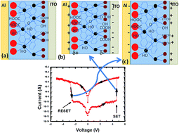
Future nanoelectronics for nonvolatile memory elements require novel materials and devices that can switch logic states with a low power consumption, minimum heat dissipation, high-circuit density, fast switching speed, large endurance and long charge retention period. Herein, we report novel high resistance resistive switching in a polar beta-polyvinylidene fluoride (β-PVDF) and graphene oxide (GO) composite. A high resistance switching ratio was achieved without the realization of the essential current-filament forming condition mainly responsible for switching the device from high to low resistance states. β-PVDF is a well known ferroelectric/piezoelectric material which changes shape and size after application of an external electric field. We propose a model which describes how the present β-PVDF–GO composite changes shape after application of an external electric field (E) which provides a favorable environment for the formation of the current linkage path of GO in the PVDF matrix. The applied positive SET electric fields (+E) switch the composite from a high to a low resistance state, which further re-switches from a low to a high resistance state under negative RE-SET electric fields (−E). The positive and negative E-fields are responsible for the contraction and expansion of β-PVDF, respectively, redox reactions between GO and adsorbed water, oxygen migrations, and/or metal diffusion from the electrode to the β-PVDF–GO matrix. The above mentioned characteristics of the composite allows switching from one high resistance state to another high resistance state. The switching current lies below the range of 10–100 μA with an exceptionally high switching ratio, which meets one of the pre-requisite criteria of low power nanoelectronics memristors.
PVDF polymer and its composite with GO are of special interest due to their possible high resistive states, nonlinear polarization, and tunable breakdown electric (E)-field dependence on the GO composition.13,14 Four different semicrystalline phases of PVDF, such as α-, β-, γ- and δ-phase exist in nature, among them the nonpolar α-phase is most stable.15 The polar β-PVDF has attracted great technological interest, with H and F atoms attached in opposite directions along the main carbon chain which develops a net dipole moment. β-PVDF is a semi-crystalline polymer that possesses high piezoelectric properties, good elastic strength and is easy to process as a film.16 The polar β-PVDF changes shape under the application of an external electric field. The polar β-PVDF and its copolymers are one potential flexible polymer ferroelectric material useful for FERAM, electro-caloric and flexo-electric applications.17 Chang et al. demonstrated the resistive switching effect in a ferroelectric BaTiO3 and GO multilayer structure and found an improved ON/OFF ratio on the order of 103 compared to basic BaTiO3.18 Poly(N-vinylcarbazole)–GO composites have been considered as the first reported example of polymer–GO based resistive switching with a high ON/OFF resistance ratio, excellent retention, and bipolar resistive switching; a similar effect was observed for the triphenylamine-based polyazomethine–GO composite.19,20 The basic mechanism behind the resistive switching in the above mentioned polymer composites has been explained on the basis of electron transfer between GO and the polymer, which in turn reduces GO under the application of an external applied electric field.
Fullerenes, carbon nanotubes, reduced graphene oxide and graphene-based systems have showed exceptionally good resistive switching in the cross-bar metal–insulator–metal (MIM) configuration, suggesting future materials for nonvolatile and tunable RRAM devices.21–23 Graphene oxide (GO) thin films and conjugated-polymer functionalized GO films have shown robust and reproducible resistive switching. Their band-structure and electronic configurations can be easily modulated by changing the chemical functionalities attached to the surface.24–27 High quality GO flakes are usually prepared by chemical oxidation of natural graphite with exfoliation into individual layers. The chemical properties of these individual layers can be significantly tuned by oxidation; one can achieve graphene with the complete removal of the carbon–oxygen (C–O) bond. The presence of hydroxyl (C–OH), epoxide (C–O–C), carboxyl (COOH), and sp2 C in the main carbon chain makes the GO flakes active for oxygen migration under the application of an external E-field.28 Redox reactions and oxygen migration have been considered important mechanisms for the possible resistive switching in GO thin films and flakes. Extensive research has been carried out to understand real mechanisms for resistive switching in GO. The common consensus about the basic mechanisms are as follows: (i) gate-metal diffusion from the gate to the bulk GO matrix, and (ii) oxygen migration/diffusion. However, till now, no tangible agreement among researchers has been achieved.29,30 Jeong et al. provided evidence of oxidized Al (i.e. formation of ultra thin Al2O3 film) near the gate (Al)–GO interface during the growth of Al by thermal evaporation, this process reduced the surface of the GO film.22 They have counter checked the role of the gate-electrode by fabrication of an inert metal gold (Au) electrode in which the resistive effect was absent and finally argued for the formation and destruction of local filaments in the thin insulating barrier near the interface between the top Al electrode and GO film rather than the bulk GO. However the ZnO nanorods embedded in the GO matrix and even GO on a flexible substrate illustrated the formation of bulk filaments under the application of a positive E-field, contrary to the Jeong report.13,31,32 In situ transmission X-ray microscopy studies on a similar system revealed that the redox reaction between GO and AlOx and the oxygen migration are responsible for resistive switching.33 The migrating oxygen ions and related filament formation by metal cations were tested for the different top and bottom metal electrodes, having different work functions with the same metal–GO–metal structure. It has been found that the capability of metal-oxide formation near the GO–metal interface is responsible for the linear and nonlinear response of GO based devices.34,35 Apart from the MIM structure, metal–GO–semiconductor (heavily doped p-Si and p-Ge) structures were also realized with resistive switching behavior.36 Samuele Porro et al. have reviewed the various aspects of the resistive switching in GO based memristor devices.37
We report a novel idea for the resistive switching mechanism where the basic matrix is a flexible piezoelectric polymer whose dimensions can be modified under the application of an external E-field. We will discuss filament-free current switching from one low current state to another nearby current state, however their ratio is very high which meets the criteria for next generation RRAM. We have critically evaluated the possible different types of conduction mechanisms involved in the β-PVDF–GO composite and their theoretical fitting with the physical constants. None of them had the ohmic behavior near the SET and RESET E-fields required for resistive switching. A model has been proposed for the oxygen migration under external and internal (in-built) E-field supported resistive switching.
The device was fabricated on an ITO coated glass substrate; the latter was first cleaned by acetone then by IPA with further ultra-sonication in acetone to remove any contamination on the ITO coated surface. A Spin-NXGM1 model spin coater was used for the thin film preparation. The spin coater was programmed to have a spinning speed of 2000 rpm for 30 seconds. Later, the grown films were annealed at 100 °C on a hot plate for 4 h to remove the solvent. The thin films of β-PVDF–GO composites with an average thickness of 120 nm were fabricated using chemical solution deposition and spin-casting techniques on an ITO/coated glass substrate. Finally, the top aluminium electrodes with a thickness of around 80 nm and a diameter of 200 μm were deposited by the thermal evaporation method using a shadow mask. All the electrical characterizations were performed on a Keithley 236 source meter with the help of microprobes at ambient conditions. A voltage–current sweep was recorded for different bias voltages across the top electrode through a LabVIEW interface program. Room temperature Raman spectra were collected over a wide range of wavelengths using a Renishaw inVia Reflex Raman Spectrometer, UK, with an excitation source of 514.5 nm and with a resolution less than 1.0 cm−1.
To obtain robust and reproducible resistive switching, first we thoroughly investigated the microstructure and crystalline quality of various β-PVDF–GO composite thin films. Fig. 2(a) shows a large area optical image obtained from one of the optimized films grown under the same conditions till a satisfactory level of average surface roughness, ∼15–20 nm, was obtained. The large uncertainties in the average surface roughness are mainly due to uneven distribution of GO in the PVDF matrix. Later the same film was examined for surface morphology and possible grain distribution or GO flake distribution in the PVDF matrix. Fig. 2(b) displays a smooth and homogeneous film with a fine distribution of GO flakes over the large area of the PVDF matrix. The SEM image rules out the formation of grains and grain boundaries and crystalline patches in the films. Raman spectroscopy studies were carried out on the PVDF–GO composite to find the crystalline qualities and β-PVDF phase and the possible defect stoichiometry in the GO in the matrix. The left hand side of the inset image of Fig. 3 shows a sharp intense Raman peak at 840.2 cm−1 suggesting the occurrence of mostly semi-crystalline β-PVDF after annealing of the spin cast film. A small amount of carbon impurities or addition of graphene or graphene related materials in any polymer matrix significantly suppresses the Raman active modes of the matrix. In the present investigation, the major Raman modes were observed from the GO in the composite matrix. The G band of graphene oxide, related to the E2g-vibration mode of sp2 carbon, was around 1596 cm−1 whereas the D band, which represents the structural defects and partially disordered structures of the sp2 domains, was at 1352 cm−1: their D/G intensity ratio was 0.88 which indicates the high quality of the GO flakes in the PVDF matrix with a reduction in the size of the in-plane sp2 domains compared to pristine graphite.39,40 The right hand side inset image of Fig. 3 shows the 2D and D + G peaks of the GO flakes, where the D/G intensity ratio for the high frequency Raman modes was 0.94, again supporting the presence of good quality GO flakes in the PVDF matrix. The SEM image and Raman spectra together confirm the homogeneous distribution of GO in the β-PVDF matrix.
![]() | ||
Fig. 2 (a) The large area optical image of the β-PVDF–GO composite, (b) SEM image indicating the homogeneous distribution of GO flakes in the PVDF matrix. |
The homogeneous β-PVDF–GO composite thin film was further investigated for the current–voltage (I–V) response under various applied E-fields (Fig. 4(a)). These devices also showed robust resistive switching with SET E-fields from 4 to 4.8 eV, however RESET E-fields were in the range from −1 to −2.4 V. The SET and RESET E-fields were independent of the switching cycles. For all cases, either sweeping started from −E to +E and back to −E or from 0 to +E to −E and back to 0, to provide a similar trend of SET and RESET behaviors of the devices. These data indicate that the composite has an envelope of SET and RESET E-fields to switch from high to low resistance states and low to high states, respectively. Fig. 4(b) shows the change in resistance (R) of the β-PVDF–GO composite under the application of an +E-field (i.e. from R ∼ 2.25 × 10¹⁰ Ω to R ∼ 8.4 × 10⁵ Ω). The magnitude of resistance even after switching lies in the megaohm region, which is the basic requirement for a next generation RRAM. Near the SET E-field, the system shows a change in resistance on the order of 104 (LRS on the order of MΩ) suggesting the composite as a potential candidate for high resistance switching elements. The nature of the increase and decrease in resistance before and after the SET E-fields, respectively, never followed the ohmic law with a slope of nearly one, indicating that a nonlinear conduction mechanism prevailed in the system. Current conduction mechanisms have been critically evaluated in the subsequent section.
Various mechanisms such as oxygen diffusion, gate-metal diffusion, and electronic trapping and de-trapping of charge carriers have been employed to support resistive switching in GO and GO-related materials.41–43 Apart from the above mechanisms, we propose a new model which might be also useful in the design of novel resistive switching systems. The model is based on the change in dimensions under the application of an external E-field. β-PVDF and its copolymers are well known piezoelectric/ferroelectric polymers, with piezoelectric coefficients of ∼20–30 pC N−1 depending on composition and stretch conditions.44,45 The physical nature of the two major elements, i.e. hydrogen and fluorine, changes the shape of the β-PVDF matrix under application of an external E-field. Positive hydrogen ions are attracted to the negative side of the E-field and repel the positive side of the E-field whereas the negative fluorine ions are attracted to the positive side of the E-field and repel the negative side of the E-field. An application of a positive E-field in the direction of the poled sample shrinks the device and hence provides a favorable path to flow the charge carriers abruptly across the heterostructure.46–49 Shrink conditions and enough potential for the small oxygen diffusion length lead to the abrupt change in the charge carriers near the SET E-fields as shown in Fig. 5(a–c). However application of a negative E-field separates/increases the diffusion length of oxygen ions and related vacancies and resets the system to HRS (Fig. 5(c)). It may be that the combined piezoelectric effect of β-PVDF and oxygen diffusion makes it possible to provide high resistance resistive switching in the composite; however a careful and in-depth investigation would be necessary to confirm this using a monolayer of β-PVDF and GO sheets/flakes. We cannot rule out other possible mechanisms responsible for conduction in the present case since a thick layer (∼120 nm) of β-PVDF–GO composite with a limited amount of in-homogeneity has been investigated.
To better understand the mechanisms involved in the conduction process, first current–voltage (I–V) switching data were fitted for Schottky emission, as shown in Fig. 6(a), in which current density can be expressed as follows:50
![]() | (1) |
![]() | (2) |
![]() | ||
Fig. 6 Current–voltage (I–V) switching data and their model fitting with (a) the Schottky-Emission (S-E), and (b) the bulk limited Poole–Frenkel (P–F) mechanism. |
To check the involvement of local (trapping and hopping) conduction process responsible for resistive switching, a trap assisted space charge limited conduction (SCLC) process was utilized to fit with the experimental data. According to SCLC theory, trap free charge carriers follow the following physical equation; where current density linearly follows the applied E-field with a slope value of nearly 2.53
![]() | (3) |
![]() | (4) |
![]() | ||
Fig. 7 Current–voltage (I–V) switching data and model fitting with the modified space charge limited conduction (SCLC) mechanism, for (a) the SET process and (b) the RESET process. |
Oxygen diffusion in GO under an E-field has been thoroughly investigated and there are well accepted mechanisms for the conduction in GO.24 It all depends on oxygen diffusion and mobility on the surface of the graphene plane.41 The oxygen diffusivity is determined from the equation: D = d2V0/[4exp(−ΔE/kBT)], where d is the jump distance of oxygen sites, ΔE is the barrier height, and V0 is the attempt frequency.42 According to the site-on-site hopping model, a decrease in barrier height and the jump distance of oxygen sites increases the oxygen diffusivity by many orders of magnitude. Suarez et al. theoretically calculated the hopping energy height of oxygen ions after removal of one electron (under a +E-field) in a graphene layer. They found that their energy lies in the range of 0.7 to 0.9 eV, however during the inclusion of an electron (under −E-field) it was nearly 0.15 eV, which suggests that the SET process is considerably slower and needs higher E-field switching compared to the RESET process.
In summary, a novel β-PVDF–GO composite with a MIM structure was successfully fabricated on an ITO coated glass substrate and demonstrated for high resistance memristive devices. Polar β-PVDF gave an extra degree of freedom to manipulate the conducting path without electroforming during switching from HRS to LRS and vice versa. A model was proposed and illustrated that, during the application of a positive E-field, the polar β-PVDF phase reduced in size due to its high piezoelectric properties, which in turn reduced the hopping path for the oxygen diffusion mainly responsible for the formation of the conductive path. Experimental current–voltage data were fitted to several conduction mechanisms, most of them failed to explain the phenomenon, however deep level trap charge assisted modified SCLC supported the conduction mechanism. The device switches from the pA to the μA current range, which may be considered a major breakthrough in the scaling-down of switching current for RRAM applications. The concept of the conduction model presented in this article may be useful in the fabrication of other forming-free RRAM devices.
This journal is © The Royal Society of Chemistry 2015 |