Band-gap tuning of graphene by Be doping and Be, B co-doping: a DFT study

Saif Ullaha, Akhtar Hussain*bd, WaqarAdil Syeda, Muhammad Adnan Saqlainc, Idrees Ahmadd, Ortwin Leenaertse and Altaf Karimf
aDepartment of Physics, International Islamic University, Islamabad, Pakistan
bTPD, Pakistan Institute of Nuclear Science and Technology (PINSTECH), P. O. Nilore, Islamabad, Pakistan. E-mail: ahmohal@yahoo.com
cDepartment of Chemistry, Quaid-i-Azam University, Islamabad, Pakistan
dDNE, Pakistan Institute of Engineering and Applied Sciences, P. O. Nilore, Islamabad, Pakistan
eDepartment Fysica, Universiteit Antwerpen, Groenenborgerlaan 171, B-2020 Antwerpen, Belgium
fCOMSATS institute of information technology, Islamabad, Pakistan

Received 1st May 2015 , Accepted 17th June 2015

First published on 17th June 2015


Abstract

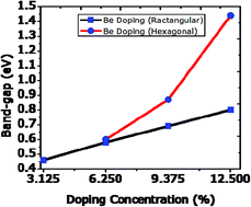
First-principles density functional theory (DFT) calculations were carried out to investigate the structural and electronic properties of beryllium (Be) doped and Be and boron (B) co-doped graphene systems. We observed that not only the concentration of impurity atoms is important to tune the band-gap to some desired level, but also the specific substitution sites play a key role. In our system, which consists of 32 atoms, a maximum of 4Be and, in the co-doped state, 2Be and 3B atom substitutions are investigated. Both dopants are electron deficient relative to C atoms and cause the Fermi level to shift downward (p-type doping). A maximum band gap of 1.44 eV can be achieved on incorporation of 4Be atoms. The introduction of Be is more sensitive in terms of geometry and stability than B. However, in opening the energy gap, Be is more effective than B and N (nitrogen). Our results offer the possibility to modify the band-gap of graphene sufficiently for utilization in diverse electronic device applications.


1. Introduction

Graphene is a one-atom-thick sp2-hybridized monolayer of carbon atoms with a two-dimensional (2D) honeycomb lattice structure and forms the building block of all other graphitic materials, such as 0D fullerenes (Bucky ball), 1D nanotubes and 3D graphite.1–4 In every graphene unit cell there are two non-equivalent carbon (C) atoms, which can be considered as two interweaving triangular sublattices, as shown in Fig. 1. Graphene is an interesting material for scientists and engineers because of its potential applications in semiconductor nanoelectronics by virtue of its remarkable physical, electrical, and optical properties.3,5–7 Graphene has tremendous charge carrier mobility of about 106 cm2 Vs−1, which is 2–3 times greater than conventional semiconductors.8
image file: c5ra08061d-f1.tif
Fig. 1 The unit cell of graphene consists of two non-equivalent sites (atoms) which are denoted by A and B where a1 and a2 denotes the primitive unit vectors.

Beside its exceptional properties, one serious issue in fabricating graphene-based transistors is its zero-gap character. For its use in semiconductor electronics, such as field-effect transistors (FETs), the opening of a band-gap is very important for switching the devices off. Consequently, the band-gap engineering9 of graphene is an essential topic with regard to applications.

Fortunately, there are certain techniques by which the band structure of graphene can be engineered. An efficient technique to induce a band-gap in graphene is to design superstructures of graphene-like nanoribbons,10,11 quantum dots,12,13 and nanomeshes.14 All these superstructures lead to quantum confinement effects, which induce a band-gap. But the fabrication of these superstructures in a controllable way is still a major challenge. The fabrication of superstructures with homogeneous widths and well defined edges under 10 nm is very difficult to achieve with top-down approaches like lithography and etching. It is easier to achieve uniform structures through bottom-up approaches,15 but the extraction procedure of patterned nanoribbons is still an issue which need to be addressed. A simple process to induce a band-gap is to adsorb graphene on an epitaxial substrate such as SiC,16 Al2O3,17 or BN.18 However it is difficult to control the morphology and adsorption energies. One of the promising alternatives to open a band-gap is the doping of graphene with suitable foreign atoms. Chemical and physical doping of graphene came into sight just after the isolation of graphene in 20045 and is now turning into a sizzling area. Jing et al.19 tested graphene, inorganic graphene analogs (IGAs) and their composites for lithium ion batteries (LIB). An excellent review regarding to the doping of graphene and derived graphene nanoribbons, graphane, graphene oxide, fluorographene, graphyne, graphdiyne, and porous graphene has been presented in ref. 20. Graphene can be doped p-type (using Al, B, NO2, H2O, and F4-TCNQ as dopants) as well as n-type (using N, and alkali metals).21–26 These dopants significantly alter the electronic structure of graphene and induce a band-gap. Substitutional doping is usually achieved with boron (B) and nitrogen (N) atoms27–33 because B and N are the closest neighbors to carbon (C).

It is desirable to dope graphene with light atoms like B, N, and oxygen (O) etc., to alter its electronic properties.23,34,35 Another light atom is Be, which has 2 valence electrons and an electronic configuration 2s22p0. Be is relatively lighter than B and obviously C atoms. At high melting temperatures of about 1500 K, Be atoms can be arranged to form an hexagonal close-packed (hpc) crystal structure. The synthesis of beryllium carbide (Be2C), which is a hard material, can be achieved by heating Be and C at about 1173.15 K. Be can also be doped in graphene by using chemical vapor deposition (CVD) techniques. Lee et al. investigated the adsorption of Be on fullerenes36 and its capacity for hydrogen (H) storage has also been investigated with ab initio calculations. These authors found that the aggregation of Be upon pure fullerene was energetically favored, causing the dissociation of H2. DFT calculations were carried out by Ferro et al.37 to investigate the absorption and diffusion of Be in graphite and the formation of Be2C. The authors found that the high absorption of Be in graphite can lead to the creation of Be2C. The structural and electronic properties of CxBem clusters were examined by Patrick et al.38 using first-principles. They argued that in bigger CxBem structures, subclusters of Be atoms can be obtained.

In the current study, an attempt has been made to achieve band-gap engineering by substitutional doping with beryllium and Be along with B in graphene sheet by increasing the doping concentration slowly and systematically. The structural properties and electronic band structures of Be and Be/B co-doped graphene are investigated using DFT calculations.

2. Details of computation

First-principles calculations were performed with the Vienna ab initio simulation package (VASP) based on density functional theory (DFT).39 The electron–ion interaction was described by the projected augmented wave (PAW)40 method and the Perdew, Burke, and Ernzerhof (PBE)41 version of the generalized gradient approximation (GGA) was adopted for the exchange and correlation parts of the electron–electron interactions. The plane-wave expansion of the wave functions was set to a kinetic energy cutoff of 450 eV. A slab model consisting of a 4 × 4 graphene supercell (32 atoms) was selected. Periodic boundary conditions are applied in all directions, so in order to avoid artificial interlayer interactions, the perpendicular distance between the layers was kept to 14 Å. Monkhorst–Pack grids are used to sample the Brillouin zone with 9 × 9 × 1 Γ-centered k mesh.42 For the density of states (DOS) a denser K-point grid of 16 × 16 × 1 was used. Energy minimizations of the structures were performed until the total Hellmann–Feynman forces were smaller than 0.01 eV Å−1. Cohesive energies were calculated using the following formula:
image file: c5ra08061d-t1.tif
in which x stands for {C, Be, B}, Ex and nx represent the atomic energy and the amount of atoms of type x, and N is the total number of atoms present in the system.

3. Results and discussions

First, a geometry optimization was performed for the pristine graphene sheet, allowing all C atoms to relax. The lattice constant and C–C bond lengths of our optimized geometry were found to be 2.46 and 1.42 Å, respectively, as can be seen in Fig. 2(a). These parameters are in good accordance with experimental values.43 The band structure of this optimized geometry was calculated and, as shown in Fig. 2(b), the conduction band minimum (CBM) and valence band maximum (VBM) are touching at the K point, forming the well-known Dirac cone. Our calculated band structure is in good agreement with previous studies in terms of gapless character and linear dispersion.3,44
image file: c5ra08061d-f2.tif
Fig. 2 The optimized geometry of a 4 × 4 supercell of graphene is depicted in part (a). The calculated band structure of this geometry is shown in part (b). The Fermi level is put to zero.

The carbon atoms in graphene can be divided into two types according to the sublattice to which they belong, and are differentiated as A (blue) and B (red) sites as shown in Fig. 3(a). In addition to this division, we found that the obtained results also strongly depend on the specific configuration of atoms to be substituted by the dopants atoms. Therefore, we have chosen two configurations of C atoms to replace, namely rectangular (denoted as R1–R4 in Fig. 3(a)) and hexagonal (referred as H1–H4 in Fig. 3(b)). In rectangular configurations, which are located on A sublattice sites (hollow transparent spheres), the upper R2 and R4 sites in Fig. 3(a) are shifted by 2.46 Å (lattice constant) along the positive x-axis direction relative to the H2 and H4 positions of the hexagonal configuration (see Fig. 3(b)).


image file: c5ra08061d-f3.tif
Fig. 3 The rectangular doping of graphene is pictured in (a) (R1–R4 blue hollow spheres). The hexagonal doping configuration is given in part (b) indicated by red hollow spheres. The high symmetry of the hexagonal doping is depicted in part (c).

Our model of graphene retains a 2D character during geometry optimization process unless the doping concentration is increased to 12.5% (4Be atoms) and co-doping of Be and B to 15.625%. A Bader charge analysis45–47 has been conducted for all the systems and it can be observed that the C atoms, being more electronegative than Be and B atoms, receive all the valence electrons. The charge transferred from either Be and/or B is largely localized on the C atoms lying in close proximity of the impurity atom.

3.1. Rectangular doping configuration

In our graphene model, 1 to 4C atoms were replaced systematically by Be atoms according to the rectangular configuration. The results are discussed in the following:
3.1.1. Doping with single Be atom. First, the graphene sheet was doped with a single Be atom making the concentration of Be 3.125% (1/32) in host graphene. We performed a geometry optimization for this system until it reached the required accuracy. The two-dimensional structure of the system was retained after the optimization procedure. When Be is substituted in a graphene sheet, it binds with three C atoms through sp2 hybridization. Due to the larger covalent radius of Be (102 pm) compared to C (75 pm), a substantial change in the bond lengths occurs. The adjoining Be–C bond lengths are increased to 1.56 Å (where C–C bond lengths are 1.42 Å in graphene). This extension in Be–C bond lengths results in a decrease of C–C bond lengths in the proximity of the Be dopant. The nearby C–C bonds are reduced to 1.38 Å as depicted in Fig. 4(a). A similar extension of 1.48 Å48 and 1.49 Å23 in B–C bond lengths was found in earlier DFT studies. The covalent radii of B (85 pm) is larger than C and smaller than Be. Therefore, one can expect the Be–C bond length to be larger.
image file: c5ra08061d-f4.tif
Fig. 4 Optimized geometry of a graphene sheet doped with single Be atom and its iso-surface plot of charge density are given in part (a) and (b), respectively. The band structure diagram is depicted in (c). STM image45 of the partial charge density is shown in part (e). Contour lines are drawn for clarity. The total and projected DOS are illustrated in part (e).

The cohesive energy of the system has been calculated to be −8.86 eV per atom which is lower than the cohesive energy of pristine graphene (−9.21 eV per atom). This value is in close agreement to the value (−9.20 eV per atom) reported by Rani and Jindal.48

The charge transfer between C and Be atoms was calculated by means of Bader charge analyses.45–47 Due to the higher electronegativity of C relative to Be, all the valence charge (2e) is transferred from Be to C atoms. A charge redistribution among the C atoms occurs with charges ranging from 3.758e to 4.515e. A higher value of charge is assigned to those C atoms which are located in the vicinity of the impurity atom. This is evident from the isosurface of the charge density distribution (see Fig. 4(b)). The white spots show charge depletion in that area. The reddish color between the C–C bonds is denser wherever charge accumulation occurs due to the charge gained (showing an increase in charge density), which is lost by impurity substitutions. However, in all the isosurface plots of doped graphene, this reddish intensity gets weaker when we move away from the impurity atoms. The charge accumulation on nearest neighboring C atoms bonded with Be can also clearly be seen in the form of white sparks in scanning tunneling microscopy (STM) images49 (see Fig. 4(d)).

The total density of states (DOS) and the projected density of states (PDOS) calculations were performed in order to further investigate the role of dopant. The results are presented in Fig. 4(e) which indicate that the Be atom's px/y orbitals (the three orbitals after sp2 hybridization of the original px and py orbitals) strongly hybridize with the px/y orbitals of carbon atoms. This strong overlapping between these p orbitals results in p–σ bonds formation near the Fermi level over an energy range from −0.5 eV to 0 eV. The pz orbitals of carbon and beryllium overlap in conduction band resulting in π bond formation. The pz orbitals of the C atoms are responsible for the DOS around the Dirac point, while the major portion of DOS at the Fermi level comes from all the 2p orbitals, but mainly from the px/y orbitals close to the dopant atom. Lastly, the DOS from C pz orbitals contribute significantly over the wide energy range except at the energy gaps at Fermi level and around the Dirac point.

We also calculated the electronic band structure for this system. As Be atoms are electron deficient, a downward shift of the Fermi level of 0.81 eV below the Dirac point occurs. In other words, Be substitution leads to p-type doping. A similar shift of 0.70 eV due to B doping in graphene has already been reported in previous studies.21,41 Moreover, the additional symmetry of the two graphene sublattices breaks due to the introduction of Be impurity. The band structure of graphene is very sensitive to the sublattice symmetry and can be altered easily by changing this symmetry. This is well illustrated by an h-BN monolayer, which has different elements on its sublattices and, consequently, exhibits a large band-gap.50 In our case, a band-gap of 0.46 eV is induced around Dirac point. Our results indicate that Be induced band-gaps are larger than those reported in previous investigations for single B and N atoms (see Table 1).

Table 1 A comparison of our results for Be with B and N doped graphene
Ref. Dopants type Dopants concentration (%) Band-gap (eV)
Our work Be 3.125 0.46
23 B 2 0.14
23 N 2 0.14
48 B 4 0.28
48 N 4 0.28


A minimal band-gap of 0.4 eV is required for suitable on/off ratios for graphene-based transistors.51 So the value of our calculated band-gap meets this requirement. Furthermore, band-gaps are generally underestimated by DFT,52,53 so the actual value of the band-gap is probably higher than our calculated value.

This remarkable result motivated us to carry out further calculations on graphene with an increasing concentration of dopants. Therefore, the graphene sheet is subsequently doped with 2, 3 and 4Be-atoms, corresponding to dopant concentrations of 6.25, 9.75 and 12.5%, respectively.

3.1.2. Doping with two Be atoms. In the following case two C atoms in graphene were replaced with Be atoms. After geometry optimization of the system, bond length increases among the various Be–C bonds were observed ranging from 1.55 to 1.57 Å, as shown in Fig. 5(a). As a result, the C–C bonds in the proximity of both the Be atoms were reduced in the range of 1.37 to 1.39 Å. The cohesive energy was found to be −8.49 eV per atom, which is smaller than for the case of a single Be atom.
image file: c5ra08061d-f5.tif
Fig. 5 The parts (a), (b) and (c) show the optimized geometry, the resulting iso-surface plot of the charge density and corresponding energy gap at Dirac point, respectively.

The valence charge released by Be is gained by the neighboring C atoms as can be seen by the isosurface plot of the charge density (Fig. 5(b)). The charge redistribution on the C atoms ranges from 3.84 to 4.77e. The average charge gained per C atom was observed to be 0.133e. Band structure calculations reveal a band-gap opening of 0.58 eV (Fig. 5(c)). On increasing the Be concentration, the resulting increase in band-gap is in agreement with previous studies for B and N doping.48

3.1.3. Doping with three Be atoms. The incorporation of three Be atoms leads to a concentration of 9.375% of Be atoms in graphene. After geometry optimization, the neighboring Be–C bonds were stretched (ranging from 1.52 Å to 1.59 Å). Consequently, compression in next neighboring C–C bond lengths occurred. These C–C bond lengths reduced to a value as low as 1.36 Å in the locality of Be atoms. The cohesive energy was found to be −8.13 eV per atom, substantially lower than for pure graphene.

Charge rearrangement on C atoms ranges from 3.78e to 5.18e. A large part of the charge from the Be atoms was gained by the nearest C atoms as shown in the isosurface plot of the charge density in Fig. 6(b).


image file: c5ra08061d-f6.tif
Fig. 6 The optimized geometry of a graphene sheet doped with three Be atoms is depicted in part (a). Isosurface plot of the charge density is shown in part (b). The calculated band structure of this optimized geometry is given in part (c).

The electronic band structure is shown in Fig. 6(c). The calculated band-gap was observed to be 0.69 eV. This gap is also higher than that reported in ref. 48 for doping with 3B and N atoms.

3.1.4. Doping with four Be atoms. The doping concentration was further increased to 12.5% by replacing 4C atoms by 4Be atoms. The Be–C bonds in the neighborhood of Be atoms were either stretched to 1.56 or 1.52 Å. The corresponding compression in C–C bonds was observed to be as low as 1.36 Å. All bond variations resulting from the optimized geometry can be seen in Fig. 7(a). The calculated cohesive energy was significantly reduced to −7.75 eV per atom vs. −9.21 eV per atom for pure graphene.
image file: c5ra08061d-f7.tif
Fig. 7 The optimized geometry of a graphene sheet doped with four Be atoms is depicted in part (a). Isosurface plot of the charge density is shown in part (b). The calculated band structure of the optimized geometry is given in part (c).

The charge relocation on the C atoms ranges from 3.91e to 4.69e and the average charge gained per C atom is 0.28e. The isosurface plot of the charge density, as shown in Fig. 7(b), shows that a major portion of the charge from the Be atoms is gained by neighboring C atoms. The band-gap increases to 0.80 eV (see Fig. 7(c)) at the Dirac point.

3.2. Hexagonal doping configuration

In addition to the impurity concentration, the actual configuration of the substituted C atoms is also an important factor that determines the value of the band-gap. As detailed below, the band-gap opening can be even higher for the same amount of Be impurities as above when different doping configurations are chosen.
3.2.1. Doping with two Be atoms. Two Be atoms were doped in the graphene sheet in such a way that both the atoms have same x-coordinate as shown in Fig. 8(a). We found that the neighboring Be–C bond lengths elongated up to 1.58 Å around the Be atoms after performing a geometry optimization. Consequently, shrinkage in the next-neighbor C–C bond lengths occurred upto 1.36 Å (Fig. 8(a)). The calculated cohesive energy was found −8.50 eV per atom for the present system. This value is very close to that calculated for 2Be atoms (−8.49 eV per atom) in the rectangular case.
image file: c5ra08061d-f8.tif
Fig. 8 The optimized geometry of a graphene sheet doped with two Be atoms (hexagonally) is depicted in part (a). Isosurface plot of the charge density is shown in part (b). The calculated band structure of this optimized geometry is presented in part (c).

As in the previous calculations, a complete transfer of the valence charge occurs from both the Be atoms to graphene. Consequently, the range of charge redistribution on C atoms takes values between 3.75 and 4.80e which is wider than that of the rectangular case (3.84 to 4.77e). The charge relocation can be seen from the isosurface plot of the charge density which shows that C atoms in the proximity of Be atoms gain a large portion of the Be valence charge (Fig. 8(b)).

The calculated band-gap is 0.6 eV, i.e. slightly larger than for the rectangular geometry (0.58 eV), with a slight shift away from the K and towards the M points of the Brillouin zone, as shown in Fig. 8(c).

From these results, it appears that the geometry of the dopant sites is important (see Fig. 3). Although the present structure has the same concentration of dopants, it is different from the system described in section 3.1.2, and consequently we observe differences in bond lengths, cohesive energy, and band-gaps. The results show that in order to obtain a higher value of the band-gap, the dopants should be incorporated in a trigonal way.

3.2.2. Doping with three Be atoms. Similar to that we did for the rectangular case, the replacement of Be atoms is now increased to 3. The neighboring Be–C bond lengths are elongated either to 1.54 or 1.6 Å after structural minimization. The expansion of the Be–C bonds is partly suppressed by the C–C bonds in close proximity to the Be atoms. These C–C bonds are contracted to 1.38 Å. The cohesive energy of the system was found to be −8.14 eV per atom which is similar to the value for rectangular case.

Charge readjustment on C atoms occurs in a range from 3.8e to 4.81e. The isosurface plot of the charge density shows that the excess charge transferred to the graphene sheet is gained by those C atoms which are bonded to Be atoms (see Fig. 9(b)).


image file: c5ra08061d-f9.tif
Fig. 9 The optimized geometry of a graphene sheet doped with three (hexagonal) Be atoms is depicted in part (a). Isosurface plot of the charge density is shown in part (b). The calculated band structure of this optimized geometry is given in part (c).

The electronic band structure calculations reveal the opening of a band-gap of 0.87 eV. The value of this calculated band-gap is higher than the observed band-gap of a graphene sheet doped with three Be atom in a rectangular way (0.69 eV). Thus a significant increase (0.18 eV) in band-gap opening occurs just due to the symmetry of the Be dopants.

3.2.3. Doping with four Be atoms. In order to find the maximum energy gap by incorporating the maximum tolerable impurity concentration, we replaced 4C atoms with Be atoms in graphene as presented in Fig. 10(a). This configuration shows a perfect hexagonal symmetry as discussed in Fig. 3(b) and (c). The Be–C neighboring bond lengths around all the Be atoms are symmetrically elongated to 1.52 Å. At the same time, compression (1.37 Å) in the C–C bonds occurred. Cohesive energy of this system is −7.72 eV per atom, which is slightly lower than the rectangular doping of 4Be atoms (−7.75 eV per atom).
image file: c5ra08061d-f10.tif
Fig. 10 The optimized geometry of a graphene sheet doped with four Be atoms (hexagonally) is depicted in part (a). Isosurface plot of the charge density is shown in part (b). The calculated band structure of this optimized geometry is given in part (c).

As in the previous cases, the whole valence charge transfers from Be to C (charge variation on C from 3.78e to 4.75e) according to a Bader analysis. The major portion of this charge is received by the neighboring C atoms of the Be as evidenced by the isosurface plot of the charge density in Fig. 10(b).

The electronic band structure shows a band-gap opening of 1.44 eV. This value of the band-gap is substantially larger (80%) than the band-gap value of 0.80 eV which was obtained for the rectangular doping of the graphene sheet with four Be atoms. This is the highest value of the gap opening that we could obtain in our calculations. This corresponds to ideal hexagonal doping as the Be atoms actually form a 2 × 2 superlattice (see Fig. 10(a)). Furthermore, an important feature of such a high symmetric case is that the bond length extensions around the Be impurities and the accompanying compressions at all positions are all the same and induce a maximum effect to open up the band-gap.

From the above presented results it can be concluded that as the substitution of C atoms by Be atoms is increased from 1 to 4 in a rectangular way, the band-gap increases linearly from 0.46 to 0.80 eV as depicted in the graph below (Fig. 11). However, the band-gap increases exponentially if the dopant substitutions are done in a hexagonal way. Although our computed values of the band-gap for Be are substantially higher than the reported values for the same concentrations of B and N by Rani and Jindal,48 the trend of increasing band gap with increased doping concentration is similar. We tried to dope beyond this concentration, but the graphene structure could not be retained during the optimization procedure. Finally, we decided to use combinations of Be and B doping with varying concentration. The obtained results are discussed in the following subsection.


image file: c5ra08061d-f11.tif
Fig. 11 The relation between Be doping concentrations and the corresponding calculated band-gaps is plotted. The linear part of graph is for rectangular doping while the exponential part occurs as a result of C atom substitutions at hexagonal positions.

3.3. Co-doping with Be and B

In this section, a combination of 1Be, 1B; 2Be, 2B and 2Be, 3B (at various positions) atoms were substituted in the graphene as co-doping in graphene is reported in earlier studies.54,55
3.3.1. One Be, one B. Here two C atoms of graphene are replaced, one with a B atom and the other with a Be atom (corresponding to a dopant concentration of 6.25%). The structural changes around the Be atom are observed to be the same as in case of single Be doping (section 3.1.1) as depicted in Fig. 12(a). The bond lengths changes are different around the B atom which is smaller compared to Be. The nearby B–C bonds are elongated to 1.48 Å, which is in a good agreement to earlier DFT studies.23,48 The next neighboring C–C bonds were reduced to either 1.41 or 1.4 Å. The B–C bonds are smaller than the Be–C bonds and larger than C–C bonds because the covalent radius of B (85 pm) is smaller than that of Be (102 pm) and larger than that of C (75 pm).
image file: c5ra08061d-f12.tif
Fig. 12 The optimized geometry of a graphene sheet co-doped with one Be and one B atom is shown in part (a). A charge density plot can be seen in part (b). The band structure of this optimized geometry is depicted in (c). Total as well as projected DOS are drawn in part (d).

The cohesive energy of the system is −8.72 eV per atom. This model has a higher cohesive energy than that of a graphene sheet doped with two Be atoms (section 3.1.2, and 3.2.1) and lower than a graphene sheet doped with a single Be atom (section 3.1.1). This shows that B atoms have better chemistry with C atoms than Be.

Because of their respective electronegativity, the valence charge, from both Be (2e) and B (3e) is transferred to the carbon atoms, and is largely concentrated on those C atoms which are closest to the impurity atoms. However, the charge redistribution range (3.72e to 5.11e) has become wider compared to simple Be replacement. The C atoms in the vicinity of B gain a larger amount of charge compared to the C atoms bonded with Be because B loses 3e. This can be seen from the isosurface plot of the charge density as depicted in Fig. 12(b).

As a matter of fact, Be and B are both electron deficient and the Fermi level undergoes a downward shift of 1.13 eV below the Dirac point. This shift is higher than that computed for only Be doping (0.81 eV). As doping with Be and B in a graphene sheet leads in both cases to hole doping, the system shows p-type behavior. As discussed above,50 the band structure can be engineered by breaking the sublattice symmetry of graphene. These dopants lead to an imbalance between the two sublattices of graphene and break the symmetry, resulting in a band-gap opening of 0.49 eV.

The results from DOS and PDOS calculations of this system are depicted in part d of the Fig. 12. The DOS around the Dirac point comes again from the pz orbital of the C atoms. Contrary to the previous case of single Be doping; where the DOS at Fermi level was only due to px/y orbitals of C and Be; here the C pz orbitals are also contributing towards DOS in addition to px/y orbitals of C and Be atoms. The main contribution to the DOS around the Fermi level comes from the C atoms bonded with the Be and B atoms. The Be atom's px/y orbitals strong hybridization with the px/y orbitals of carbon atoms results in p–σ bonds formation near the Fermi level over an energy range from −0.5 eV to 0 eV (similar as in sec. 3.1.1). Similarly, π bond formation just below the Dirac point comes from some overlapping of the pz orbitals of carbon and beryllium atoms. The B atom has very small contributions to the DOS around the Fermi level. Nevertheless, the B 2px/y orbitals have strong hybridization with C 2px/y orbitals in the energy range from −2.5 to −1.7 eV, where p–σ bonds formation occurs. A minor overlapping can also be seen at some points between pz orbitals of C and B in the valance and the conduction band region (Fig. 12(d)).

3.3.2. Two Be, two B. Co-doping with two Be and two B atoms makes the total concentration of the impurities 12.5% in the host graphene. The bonds around Be atoms are either enlarged to 1.57 or 1.52 Å after geometry optimization. The B–C bond lengths are found to be 1.44 Å, and 1.42 Å. The next neighboring C–C bonds in the vicinity of Be and B, on the other hand, are reduced to lower values (with a range from 1.37 to 1.39 Å). The changes in the bond lengths can be seen in Fig. 13(a). The system has a cohesive energy of −8.19 eV per atom, which is higher than the cohesive energy of graphene doped with four Be atoms (−7.75 eV per atom). Thus C–B bonds are stronger relative to C–Be bonds.
image file: c5ra08061d-f13.tif
Fig. 13 The optimized geometry of a graphene sheet co-doped with two Be atoms and two B atoms is depicted in part (a). Isosurface plot of the charge density is shown in part (b). The calculated band structure of this optimized geometry is given in part (c).

The variation of the charge observed on the C atoms is in the range from 3.83e to 4.95e. The average charge per C atom is increased to 0.36e. Most of the charge which is transferred to graphene is acquired by those C atoms which are bonded with impurity atoms (Be, B). The neighboring C atoms of B attained greater amount of charge as compared to the C atoms bonded with Be atoms, as can be seen from the isosurface plot of the charge density (see Fig. 13(b)). The band structure calculations reveal a band-gap opening of 0.99 eV. The band structure diagram is depicted in Fig. 13(c). This value of the band-gap is higher than in the case of doping with 4Be atoms in a rectangular way and lower than in the hexagonal case.


3.3.3.1. Two Be, three B (pattern I). Co-doping with 2Be and 3B atoms makes the total concentration of the impurities 15.625% in the host graphene. To incorporate the site effect, three mechanisms were investigated by varying the dopant position of one of the three B atoms. In pattern I, two Be atoms and two of the three B atoms are incorporated on the same sublattice while the third B atom is integrated on the other sublattice, as depicted in Fig. 14(a). The bonds in the proximity of the Be atoms are enlarged to either 1.52 or 1.57 Å after geometry optimization. Variations in the B–C neighboring bonds range from 1.41 to 1.5 Å (see Fig. 14(a)). The cohesive energy of this model is −8.07 eV per atom, which is significantly higher than a graphene sheet doped with four Be atoms (−7.75 eV per atom). This shows that due to B insertion, the graphene structure is less destabilized than by Be substitution.
image file: c5ra08061d-f14.tif
Fig. 14 The optimized geometry of a graphene sheet co-doped with two Be atoms and three B atoms (pattern I) is depicted in part (a). Isosurface plot of the charge density is shown in part (b). The calculated band structure of this optimized geometry is given in part (c).

The charge redistribution on the C atoms is seen to range from 3.89e to 5.17e. The isosurface plot of the charge density shows more local charge density near those C atoms which are bonded with B atoms as compared to those which are in the locality of Be atoms (see Fig. 14(b)). The average charge gain per C atom is 0.48e. This is the highest value of charge gained per C atom.

A band-gap opening of 0.64 eV is observed. The value of this band-gap is smaller than the band-gap value obtained for a graphene sheet co-doped with two Be atoms and two B atoms. This decrease is understandable because one of the B atoms was incorporated at a different sublattice compared to the other impurity atoms, which results in a smaller value of the band-gap.48 The band structure diagram is shown in Fig. 14(c).


3.3.3.2. Two Be, three B (pattern II). In the next part, the graphene sheet is doped with the same concentration of the same impurity atoms (as in upper case). However, the location of one B atom is changed such that the x-coordinates of all three B atom are the same. The relaxed Be–C neighboring bond lengths are stretched to values ranging from 1.51 to 1.57 Å as shown in Fig. 15(a). The B–C inter-atomic bonds were found to be in the range of 1.44 to 1.46 Å. The cohesive energy of the system is −8.03 eV per atom a bit lower than the system discussed above.
image file: c5ra08061d-f15.tif
Fig. 15 The optimized geometry of a graphene sheet co-doped with two Be atoms and three B atoms (pattern II) is depicted in part (a). Isosurface plot of the charge density is shown in part (b). The calculated band structure of this optimized geometry is given in part (c).

The valence charge from the impurity atoms on the C atoms ranges from 3.87e to 5.95e. Two C atoms which are packed within B atoms have a larger value of accumulated charge (5.95e and 5.84e) as shown in the isosurface plot of the charge density (see Fig. 15(b)).

Band structure calculations show a band-gap opening of 0.96 eV. The value of the band-gap is higher than the one observed for the above system because all the dopants are incorporated at same sublattice sites. The band structure diagram is depicted in Fig. 15(c).


3.3.3.3. Two Be, three B (pattern III). In this new configuration the position of one B atom is changed relative to the previous configuration, as shown in Fig. 16(a). This makes all impurity atoms reside on the same sublattice sites. The stretching of the Be–C bonds in the neighborhood of the Be atoms are in the range of 1.52 to 1.57 Å and the B–C bonds are lengthened up to 1.53 Å. The cohesive energy of the system is −8.06 eV per atom, similar to the above reported patterns I and II (Fig. 17).
image file: c5ra08061d-f16.tif
Fig. 16 The optimized geometry of a graphene sheet co-doped with two Be atoms along with three B atoms (pattern III) is depicted in part (a). Isosurface plot of the charge density is shown in part (b). The calculated band structure of this optimized geometry is given in part (c).

image file: c5ra08061d-f17.tif
Fig. 17 The relation between the band-gap and co-doped concentration of Be and B (left panel). Only the pattern with the highest value of the band-gap is shown here. In the right panel, the variation in cohesive energy with change in doping concentration and position is depicted. The lowest cohesive energy corresponds to 4Be atoms doping hexagonally against the highest value of (1.44 eV) energy gap.

In this case we found a maximum charge of 7.09e on the C atom that is sandwiched between Be and B. This huge charge accumulation can also be nicely observed around the C atoms (the reddish line) near the lower Be atom in Fig. 16(b). Similarly, some C atoms retain a minimum charge of 2.63e. Thus the charge redistribution range is much wider relative to previous cases. This fact is also reflected by the isosurface charge density plot in Fig. 16(b).

The value of the band-gap is observed to be 1.12 eV as depicted in Fig. 16(c); the 2nd highest value we observed in this study. We can conclude that the present pattern with an impurity concentration of 15.625% yields the maximum band-gap value accompanied with maximum distortion in the geometric structure and charge relocation.

All our results are summarized in Table 2. By increasing the impurity concentration, the value of the band-gap increases but at the same time the value of the cohesive energy decreases, indicating a decrease in the stability of the structure as compared to a pristine graphene sheet. Graphene sheets co-doped with Be and B have higher cohesive energies as compared to that of Be doping only. This is because the covalent radius of B is closer that of C. Therefore, the bonds distort little as compared to Be, as illustrated by the variations of the bond lengths.

Table 2 Summary of the results obtained for Be, and, Be/B co-doping in graphenea
Dopants types Concentration (%) Pattern Cohesive energy (eV per atom) Band-gap (eV)
a The cohesive energy of pristine graphene was calculated to be −9.21 eV per atom.
1Be 3.125 Rectangular −8.86 0.46
2Be 6.25 Rectangular −8.49 0.58
3Be 9.375 Rectangular −8.13 0.69
4Be 12.5 Rectangular −7.75 0.80
2Be 6.25 Hexagonal −8.50 0.60
3Be 9.375 Hexagonal −8.14 0.87
4Be 12.5 Hexagonal −7.72 1.44
1Be, 1B 6.25 Same sublattice sites −8.72 0.49
2Be, 2B 12.5 Same sublattice sites −8.19 0.99
2Be, 3B 15.625 Different sublattice sites (pattern I) −8.07 0.64
2Be, 3B 15.625 Same sublattice sites (pattern II) −8.03 0.96
2Be, 3B 15.625 Same sublattice sites (pattern III) −8.06 1.12


4. Conclusions

First-principles DFT calculations were performed to investigate the structural and electronic properties of graphene systems doped with Be and co-doped with Be and B. Graphene was doped with Be atoms at different sites with varying concentration ranging from 1–4 per 4 × 4 graphene supercell. Be doping can significantly modify the electronic and structural properties of graphene. Replacement of a single C atom with a Be atom induces a band-gap of 0.46 eV, which seems sufficient for its use in transistor applications because graphene based FETs required a minimum band-gap of 0.4 eV51 for useful on/off ratios. The shift in Fermi level indicates p-type doping. We studied two configurational symmetries for the dopants, namely rectangular and hexagonal. By an increase in the impurity concentration, a linear rise in the band-gap was observed for rectangular doping. However, an exponential rise (max. value 1.44 eV) was observed for hexagonal doping, proving the superiority of hexagonal doping over rectangular (replacement sites dependency). Co-doping with a second species, namely B, with Be was investigated too. The structure remains intact up to 5 impurity atoms (2Be and 3B) in contrast to doping with only Be atoms in which case only 4 atoms can be tolerated. The position of the B atoms was varied in the structure to check for site-dependent variations in the energy gap. A wide variation in the band-gap from 0.64 to 1.12 eV was observed which illustrates the significance of the doping sites. A lower value of the energy gap resulting from co-doping indicates that pure Be is more efficient in inducing band-gaps. It was also found that because of their higher electronegativity, C atoms receive all the valence electrons of the Be and Be atoms. These electrons mainly accumulate on the C atoms closest to the Be and B atoms. Finally, increasing the impurity concentration leads to a decrease in cohesive energy of the system, indicating weakening the bonds. Our results offer the opportunity to tailor the electronic band structure of graphene up to desired level and allow its use in wide spread applications of electronic devices.

Acknowledgements

We are thankful to Dr Arshad Farhan, Dr Shafqat Hussain Shah and Dr Saqib Javed for their time to time valuable suggestions and discussions.

References

  1. P. R. Wallace, Phys. Rev., 1947, 71, 622 CrossRef CAS .
  2. R. Saito, G. Dresselhaus and M. S. Dresselhaus, Physical Properties of Carbon nanotubes, Imperial College Press, London, UK, 1998 Search PubMed .
  3. A. K. Geim and K. S. Novoselov, Nat. Mater., 2007, 6, 183 CrossRef CAS PubMed .
  4. A. H. C. Neto, F. Guinea, N. M. R. Peres, K. S. Novoselov and A. K. Geim, Rev. Mod. Phys., 2009, 81, 109 CrossRef .
  5. K. S. Novoselov, A. K. Geim, S. V. Morozov, D. Jiang, Y. Zhang, S. V. Dubonos, I. V. Gregorieve and A. A. Firsov, Science, 2004, 306, 666 CrossRef CAS PubMed .
  6. K. S. Novoselov, A. K. Geim, S. V. Morozov, D. Jiang, M. I. Katsnelson, I. V. Grigorieva, S. V. Dubonos and A. A. Firsov, Nature, 2005, 197, 438 Search PubMed .
  7. A. K. Geim, Science, 2009, 324, 1530 CrossRef CAS PubMed .
  8. E. V. Castro, H. Ochoa, M. I. Katsnelson, R. V. Gorbachev, D. C. Elias, K. S. Novoselov, A. K. Geim and F. Guinea, Phys. Rev. Lett., 2010, 105, 266601 CrossRef .
  9. K. S. Novoselov, Nat. Mater., 2007, 6, 720 CrossRef CAS PubMed .
  10. M. Y. Han, B. Ozyilmaz, Y. Zhang and P. Kim, Phys. Rev. Lett., 2007, 98, 206805 CrossRef .
  11. X. Li, X. Wang, L. zhang, S. Lee and H. Dai, Science, 2008, 319, 1229 CrossRef CAS PubMed .
  12. L. A. Ponomarenko, F. Schedin, M. I. katsnelson, R. Yang, E. W. Hill, K. S. Novoselov and A. K. Geim, Science, 2008, 320, 356 CrossRef CAS PubMed .
  13. B. Trauzettel, D. V. Bulaev, D. Loss and G. Burkard, Nat. Phys., 2007, 3, 192 CrossRef CAS PubMed .
  14. J. Bai, X. Zhong, S. Jiang, Y. Huang and X. Duan, Nat. Nanotechnol., 2010, 5, 190 CrossRef CAS PubMed .
  15. J. Cai, P. Ruffieux, R. Jaafar, M. Bieri, T. Braun, S. Blankenburg, M. Muoth, A. Seitsonen, M. Saleh, X. Feng, K. Mullen and R. Fasel, Nature, 2010, 466, 470 CrossRef CAS PubMed .
  16. S. Y. Zhou, G.-H. Gweon, A. V. Fedorov, P. N. First, W. A. d. Heer, D.-H. Lee, F. Guinea, A. H. C. Neto and A. Lanzara, Nat. Mater., 2007, 6, 770 CrossRef CAS PubMed .
  17. B. Huang, Q. Xu and S. Wei, Phys. Rev. B: Condens. Matter, 2011, 84, 155406 CrossRef .
  18. G. Giovannetti, P. A. khomyakov, G. Brocks, P. J. Kelly and J. v. d. Brink, Phys. Rev. B: Condens. Matter, 2007, 76, 073103 CrossRef .
  19. Y. Jing, Z. Zhou, C. R. Cabrera and Z. Chen, J. Mater. Chem. A, 2014, 2, 12104 CAS .
  20. Q. Tang, Z. Zhou and Z. Chen, Nanoscale, 2013, 5, 4541 RSC .
  21. P. A. Denis, Chem. Phys. Lett., 2010, 492, 251 CrossRef CAS PubMed .
  22. A. Lherbier, X. Blasé, Y.-M. Niquet, F. Triozon and S. Roche, Phys. Rev. Lett., 2008, 101, 036808 CrossRef .
  23. M. Wu, C. Cao and J. Z. Jiang, Nanotechnology, 2010, 21, 505202 CrossRef CAS PubMed .
  24. E. H. Hwang, S. Adam and S. D. Sarma, Phys. Rev. B: Condens. Matter Mater. Phys., 2007, 76, 195421 CrossRef .
  25. O. Leenaerts, B. Partoens and F. M. Peeters, Phys. Rev. B: Condens. Matter Mater. Phys., 2008, 77, 125416 CrossRef .
  26. H. Pinto, R. Jones, J. P. Goss and P. R. Briddon, J. Phys.:Condens. Matter, 2009, 21, 402001 CrossRef CAS PubMed .
  27. L. S. Panchakarla, K. S. Subrahmanyam, S. K. Saha, A. Govindaraj, H. R. Krishnamurthy, U. V. Waghmare and C. N. R. Rao, Adv. Mater., 2009, 21, 4726 CAS .
  28. D. Wei, Y. Liu, Y. Wang, H. Zhang, L. Huang and G. Yu, Nano Lett., 2009, 9, 1752 CrossRef CAS PubMed .
  29. Y. Fan, M. Zhao, Z. Wang, X. Zhang and H. Zhang, Appl. Phys. Lett., 2011, 98, 083103 CrossRef PubMed .
  30. X. Fan, Z. Shen, A. Q. Liu and J.-L. Kuo, Nanoscale, 2012, 4, 2157 RSC .
  31. A. K. Manna and S. K. Pati, J. Phys. Chem. C, 2011, 115, 10842 CAS .
  32. D. H. Wu, Y. F. Li and Z. Zhou, Theor. Chem. Acc., 2011, 130, 209 CrossRef CAS .
  33. Y. Li, Z. Zhou, P. Shen and Z. Chen, ACS Nano, 2009, 3, 1952 CrossRef CAS PubMed .
  34. F. Cervantes-Sodi, G. Csanyi, S. Piscanec and A. C. Ferrari, Phys. Rev. B: Condens. Matter Mater. Phys., 2008, 77, 165427 CrossRef .
  35. B. Biel, F. Triozon, X. Blase and S. Roche, Nano Lett., 2009, 9, 2725 CrossRef CAS PubMed .
  36. H. Lee, B. Huang, W. Duan and J. Ihm, J. Appl. Phys., 2010, 107, 084304 CrossRef PubMed .
  37. Y. Ferro, A. Allouche and C. Linsmeier, J. Appl. Phys., 2013, 113, 213514 CrossRef PubMed .
  38. A. Patrick, P. Williams and E. Blaisten-Barojas, J. Mol. Struct.: THEOCHEM, 2007, 824, 39 CrossRef CAS PubMed .
  39. G. kresse and J. Hafner, Phys. Rev. B: Condens. Matter Mater. Phys., 1994, 49, 14251 CrossRef CAS .
  40. P. E. Blochl, Phys. Rev. B: Condens. Matter Mater. Phys., 1994, 50, 17953 CrossRef .
  41. J. P. Perdew, K. Burke and M. Ernzerhof, Phys. Rev. Lett., 1996, 77, 3865 CrossRef CAS .
  42. H. Monkhorst and J. Pack, Phys. Rev. B: Solid State, 1976, 13, 5188 CrossRef .
  43. D. R. Cooper, B. D'Anjou, N. Ghattamaneni, B. Harack, M. Hilke, A. Horth, N. Majlis, M. Massicotte, L. Vandsburger, E. Whiteway and V. Yu, ISRN Condens. Matter Phys., 2012, 2012, 56 Search PubMed.
  44. S. M. Kozlov, F. Vines and A. Gorling, Adv. Mater., 2011, 23, 2638 CrossRef CAS PubMed .
  45. W. Tang, E. Sanville and G. Henkelmen, J. Phys.: Condens. Matter, 2009, 21, 084204 CrossRef CAS PubMed .
  46. E. Sanville, S. D. Kenny, R. Smith and G. Henkelman, J. Comput. Chem., 2007, 28, 899 CrossRef CAS PubMed .
  47. G. Henkelman, A. Arnaldsson and H. Jonsson, Comput. Mater. Sci., 2006, 36, 354 CrossRef PubMed .
  48. P. Rani and V. K. Jindal, RSC Adv., 2013, 3, 802 RSC .
  49. D. E. P. Vanpoucke and G. Brocks, Phys. Rev. B: Condens. Matter Mater. Phys., 2008, 77, 241308(R) CrossRef .
  50. X. Blase, A. Rubio, S. G. Louie and M. L. Cohen, Phys. Rev. B: Condens. Matter Mater. Phys., 1995, 51, 6868 CrossRef CAS .
  51. F. Schwierz, Nat. Nanotechnol., 2010, 5, 487 CrossRef CAS PubMed .
  52. C. S. Wang and W. E. Pickett, Phys. Rev. Lett., 1983, 51, 597 CrossRef CAS .
  53. M. K. Y. Chan and G. Ceder, Phys. Rev. Lett., 2010, 105, 196403 CrossRef CAS .
  54. P. A. Denis, C. P. Huelmo and F. Iribarne, Comput. Theor. Chem., 2014, 1049, 13 CrossRef CAS PubMed .
  55. P. A. Denis and C. P. Huelmo, Carbon, 2015, 87, 106 CrossRef CAS PubMed .

This journal is © The Royal Society of Chemistry 2015
Click here to see how this site uses Cookies. View our privacy policy here.