
An amorphous barium titanate thin film improves light trapping in Si solar cells
A. K. Sharmaab,
B. Geetha Priyadarshini*ac,
B. R. Mehtaa and
Dinesh Kumard
aThin Film Laboratory, Department of Physics, Indian Institute of Technology Delhi, India
bNational Centre for Photovoltaic Research & Education, Indian Institute of Technology Bombay, India
cNanotech Research Innovation & Incubation Centre, PSG Institute of Advanced Studies, Peelamedu, Coimbatore-641004, Tamil Nadu, India. E-mail: bgp@psgias.ac.in; geethapriyadarshini@gmail.com; Fax: +91-422-257-3833; Tel: +91-98438-21434, +91-422-434-4000 ext. 4193
dTATA Power Solar System Limited, Bangalore, India
First published on 1st July 2015
Abstract
A new anti-reflection coating based on amorphous barium titanate (a-BTO) was developed using RF magnetron sputtering technique. Systematic studies on the structural and optical properties were carried on a-BTO thin films deposited on polished Si and textured Si substrates. In the visible range of the solar spectrum, the refractive index was found to be 2.02–1.91 with high transmittance of greater than 85%. Maximum reduction in the reflectance for a-BTO on polished Si and textured Si substrates was found to be 100% (at 550 nm) and 85% (at 400 nm), respectively. Further, improvement in cell efficiency of a Si solar cell with a-BTO anti-reflection coating was found with an increase from 9.3% to 10% accompanied by improvements in overall performance parameters such as short circuit density (Jsc), open circuit voltage (Voc) and fill factor (FF). These results indicate that an a-BTO thin film deposited using RF magnetron sputtering can be used as an alternative anti-reflection coating for Si based photovoltaic cells.
1. Introduction
Barium titanate (BTO) is among the most extensively studied systems in the perovskite class of materials. During cooling from high temperatures, BTO transforms from a highly symmetric paraelectric cubic phase to a slightly distorted ferroelectric structure with tetragonal, orthorhombic and rhombohedral symmetries at low-temperature.1 Due to this phase transformation, BTO materials in bulk form, multi-layers, thin films and nanostructures share a variety of applications possessing exceptional dielectric, ferroelectric and piezoelectric properties.2–6Over the years, anomalous high photovoltages are observed in BTO which show potential for photovoltaic (PV) associated routes of energy generation through various conduction mechanisms. The photovoltaic effect in bulk and single crystal BTO was found to depend on the chemical composition, and grain size.7 One of the early reports by Chynoweth revealed the presence of space charge-fields and potential variations across the crystals are responsible for associated photovoltaic effect in single crystal BTO.8 High photovoltage resulted from the integration of small photovoltage across spontaneously polarized individual BTO grains.9 Recently, Yang et al.10 reported that the photovoltages are significantly higher than the bandgap of ferroelectric materials and the electric-field control over domain structure allows the photovoltaic effect to be reversed in polarity or when turned off. Cudney et al. observed generation of photogalvanic current at least two trap levels with two different strengths when the BTO crystal was illuminated by a spatially periodic light intensity pattern.11 Xing et al. stated the reasons for large generation of photovoltage in BTO/Si heterojunction structure due to the low oxygen content and migration of oxygen vacancies leading to better conductivity.12 Shift current is yet another dominant mechanism in bulk BTO as photocurrent does not only depend on the magnitude of material polarization, but also on electronic states with delocalized, covalent bonding that is highly asymmetric along the current direction.13 However, nanometer-sized BTO glass has wider transmittance window 250 nm–11![[thin space (1/6-em)]](https://www.rsc.org/images/entities/char_2009.gif) 000 nm and high refractive index ∼2.15 which offers lower reflectance to the Si based photovoltaic devices.14 Amorphous BTO thin films of 140 nm thick deposited using metalorganic chemical vapor deposition was reported to show high optical transmittance of 80% with optical band gap of 4.71 eV in the visible wavelength range.15
000 nm and high refractive index ∼2.15 which offers lower reflectance to the Si based photovoltaic devices.14 Amorphous BTO thin films of 140 nm thick deposited using metalorganic chemical vapor deposition was reported to show high optical transmittance of 80% with optical band gap of 4.71 eV in the visible wavelength range.15
Light trapping is essential in order to achieve complete absorption of light in the Si solar cell. A commercial crystalline Silicon (c-Si) solar cell has 180 μm thickness with typical feature size of the texturing is in the range of 5–10 μm.16 At the front side, they are covered with a pyramidal light-trapping texture coated with an 80 nm-thick Si3N4 antireflection layer.17 Antireflection coating (ARC) enhances the absorption of photons through reduction in reflection thereby increasing the short circuit current density (Jsc) that translates into increase in solar cell efficiency. Ideal broadband anti-reflection requires complete removal of impedance mismatch that is possible when a dispersive, graded refractive index medium is used as impedance matching layer.18
In this paper, we investigate the potential of a-BTO thin film coatings for light trapping in Si solar cells which could be an alternative for existing anti-reflection coating like Si3N4, TiO2 and MgF2 etc. in near future. Therefore, the present study focuses on the development of a-BTO thin-films on polished and textured Si substrate with enhanced antireflection properties for improving Si solar cell performance by efficiently trapping visible light. The vital physical properties required for antireflection coating such as refractive index, and transmittance was evaluated for a-BTO thin film. The performance improvement in conventional monocrystalline silicon n+–p diffused junction solar cell for a-BTO coating is also discussed in detail.
2. Experimental details
2.1 Synthesis and characterization of antireflection BTO thin films
In this study BTO thin-films were deposited on the quartz glass, polished Si (n type and p type), textured Si and bare Si solar cells using rf-magnetron sputtering of BaTiO3 target (99.99% purity). The deposition conditions are tabulated in Table 1.| Specification | Particulars |
|---|---|
| Base pressure (Torr) | 1.5 × 10⁻⁵ |
| Deposition pressure (mTorr) | 7.5 |
| RF power (W) | 100 |
| Ar:O2 ratio (sccm) |
20:0, 16:4, 10:10 and 0:20 |
| Deposition temperature (°C) | 30, 500 |
| Deposition time (sec) | 300 |
The structural properties of BTO thin films were investigated using glancing incidence X-ray diffraction (GIXRD) and high-resolution transmission electron microscopy (HRTEM). The optical constants (n, k) and thickness (t) of thin-films was estimated using the M-2000F ellipsometer (J. A. Woollam Co., Inc). The reflectance and transmittance of barium titanate thin films deposited on different substrates was carried out using UV/Vis spectrophotometer (Perkin-Elmer Lambda 35) with an integrating sphere detector.
2.2 Solar cell fabrication and characterization
Boron doped CZ Si wafers of size 125 × 125 mm with thickness 200 ± 10 μm and bulk resistivity in the range of 0.5–3 Ω cm were used as the starting material for the solar cell fabrication. Solar cells were fabricated by the conventional silicon solar cell process with screen print technology. The saw damages and the residual contamination were removed by alkaline chemicals (NaOH, 40% vol/vol at 80 °C for 30 s) followed by alkaline texturization (NaOH, 4% vol/vol, 85 °C for 15 min). Consecutively, P-diffusion was carried out by using POCl3 in a tube furnace. The diffusion was carried out at 880 °C for 40 min to form a shallow junction (∼0.3 micron junction depth). The phosphosilicate glass formed during diffusion process was removed in buffered HF (10% HF for 2 min) followed by plasma based edge isolation. The front and back contacts were made by using conventional screen print technology and simultaneously co-fired to realize the ohmic contacts on the front surface as well as aluminium (Al) back surface field (BSF) on the back surface.In order to evaluate the solar cell performance, the measurements were carried out with (test cell) and without (control cell) a-BTO coating on monocrystalline Si solar cells under one sun (100 mW cm−2) using standard solar spectrum AM 1.5G. The performance parameters such as short circuit current density (Jsc), open circuit voltage (Voc), fill factor (FF), series resistance (Rs) and shunt resistance (Rsh) were calculated from illuminated current density–voltage (J–V) characteristics. Also, solar cell collection efficiency in 400–1100 nm wavelength range was obtained with internal quantum efficiency (IQE) i.e. incident photon to converted electron ratio (IPCE) measurement.
3. Results and discussion
3.1 Structural properties
The structural characterization of sputtered BTO thin-films was done using X-ray diffraction (XRD) at glancing angle 0.5°. Fig. 1 shows the GIXRD pattern of as-deposited BTO thin-films deposited on Si substrate held at 500 °C and with different Ar to O2 ratios. There is no distinct peak signifying the amorphous phase formation due to relatively high deposition temperature of 500 °C at which crystallization is likely to take place. Crystalline peaks of BaTi2O5 emerge in the amorphous background at 2θ = 25°and very low intensity peaks of BaTiO3 co-exists with the BaTi2O5 phase at higher O2 flow rates. Presence of BaTiO3 peaks in XRD profiles indicates that increase in O2 flow rate during deposition favors nucleation of BaTiO3 crystals in deposited thin films. When Ar to O2 ratio was increased to 16:4, co-existence of BaTiO3 and BaTi2O5 phases was observed. For this particular sample, refractive indices were calculated to be 2.42 and 2.15, respectively which might play a major role in minimising the reflection losses. Therefore, for the present study on light trapping, BTO thin films deposited at Ar to O2 gas ratio of 16:4 is chosen. Subsequently, BTO films with Ar:O2 ratio of 16:4 sccm were deposited at room temperature (30 °C) to obtain amorphous phase on different substrates.
 | ||
| Fig. 1 GIXRD pattern of BTO thin films deposited at 500 °C on Si substrate with Ar:O2 gas ratios of (a) 20:0 sccm, (b) 16:4 sccm, (c) 10:10 sccm and (d) 0:20 sccm. | ||
Fig. 2(a) shows the GIXRD patterns for BTO thin films deposited on different Si substrates such as p-Si, n-Si, textured Si and multi-crystalline Si. BTO thin films were predominantly amorphous around 2θ ranging from 25°–30° when deposited at room temperature which is desired for the present work. It is important to point out here, that at present it is difficult to comment on the formation of single phase a-BaTiO3 or a-BaTi2O5 or both (a-BaTiO3 and a-BaTi2O5) in the as-deposited films on different substrates. But it is certain from the XRD profile that the film structure is comprised of both the amorphous and nanocrystals of barium titanate with a broad peak centered at 2θ = 55°.
 | ||
| Fig. 2 BTO thin films (a) GIXRD pattern deposited with Ar:O2 :: 16:4 at room temperature on different substrates; (b) TEM image with SAED pattern (in inset); (c) digital photograph of dark blue coating on textured and polished Si substrates. | ||
Fig. 2(b) shows HRTEM image and corresponding selected are electron diffraction pattern (SAED) consists of broad diffused ring without the presence of bright spots confirming the amorphous nature of BTO film. Despite the presence of amorphous BTO and nanocrystal BTO phase revealed by XRD analysis, a single diffused ring corresponding to glassy phase is obtained possibly due to similar d-spacing of BaTiO3 and BaTi2O5.
Fig. 2(c) is a digital photograph of sputtered a-BTO thin-films on textured (Tx) and polished (P) silicon substrates showing dark bluish colored coatings.
3.2 Optical properties
Major inference can be drawn on anti-reflection properties of the developed coatings by measuring refractive index, transmittance and reflectance values. Ellipsometric studies on broadband, omnidirectionally, and polarization-insensitivity of antireflection coatings were examined systematically and further supported by UV-Vis spectrophotometric studies.Fig. 3(a) shows the refractive index (n), extinction coefficient (k) and real & imaginary parts of the dielectric function (e1, e2) of deposited amorphous BTO thin films. The n value was found to be 2.02 at 400 nm and decreased to 1.89 at 1000 nm and varied from 1.98–1.92 in the range 450–650 nm where maximum photon flux in the entire solar spectrum is available for energy conversion. These values of n agree with the requirement for ideal conditions of silicon solar cell based module.19 The extinction coefficient (k) value found to be 0.009 at 400 nm and increased to a maximum value of 0.015 at 380 nm and then decreased to 0.000 at 1000 nm. In addition, e1 decreased from its highest value 4.01 (at 400 nm) to 3.58 (at 1000 nm), whereas e2 decreased from maximum value of 0.062 (at 486 nm) to a minimum value of 0.00 (at 1000 nm). The loss factor e2/e1 shows maximum dielectric loss in the 400–700 nm and almost zero loss beyond 750 nm. This observation emphasize that the visible portion holds greater dielectric loss in comparison to near infrared radiation of the spectrum signifying the potential of a-BTO layer as the anti-reflection coating in the maximum photon flux available in the solar spectrum.
 | ||
| Fig. 3 (a) Optical constant (n, k) and dielectric constant (e1, e2); (b) relative reduction in reflectance, transmittance for a-BTO thin-films deposited on polished & textured Si substrate, quartz substrate, respectively; in 400–1000 nm wavelength range. | ||
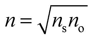
To achieve an optimal anti-reflection effect resulting in zero net reflection in the spectral range of interest 450–650 nm, the amplitudes of the reflected beam at the air-coating interface and coating-substrate interface has to be equal and exactly one-half wave (180°) out of phase, resulting in destructive interference. The first condition can be met when refractive index of the coating (n) equals to the square root of the product of the refractive indices of substrate (ns) and medium (no) expressed by eqn (1)20
 | (1) |
The second condition is that the optical thickness of the ARC layer must be close to a quarter of the wavelength at which zero reflectance should occur (i.e., the reflected wave must be out of phase by π). This condition is expressed by eqn (2):
 | (2) |
Fig. 3(b) shows the percentage reduction in the transmittance for a-BTO coated quartz substrate and reflectance for a-BTO antireflection coating on polished Si and textured Si substrates as function of the wavelength. The transmittance value 85–95% in the wavelength range 400–1100 nm shows acceptance of a-BTO coating as a wide transmission window layer for the solar cell application. Recently, Masuno et al. reported wide transmission range in bulk counterpart of BTO glass in the wavelength range of 370 nm to 7.7 μm.22 The measured transmittance values ensure the merit of transparency for the proposed a-BTO antireflection coating for Si solar cells. The relative reduction in the reflectance shown in Fig. 3(b) emphasize that the reflectance values are reduced for the entire wavelength range corresponds to the reflectance values for the bare substrates (not shown here). For a-BTO coated polished Si substrate, zero reflectance was observed at 550 nm, which depict that 100% relative reduction in reflectance values of bare substrate. However, for a-BTO coated textured Si substrate, the minimum reflectance was found at 400 nm value and shows as 85% relative reduction in pristine reflectance. The observed shift in wavelength value for minimum reflectance in polished Si (at 550 nm) and textured Si (at 400 nm) is possibly due the multiple reflection phenomenon taking place at the interface of a-BTO coating and textured Si substrate.
Typically, the surface of solar cell is textured in order to avoid photon loss due to multiple reflections. Therefore, in present study the solar cell surface assumed to be similar to the of textured Si surface as described in the experimental section.
3.3 Solar cell performance
Fig. 4(a) shows the illuminated I–V characteristics and Table 2 illustrate the performance parameters of control and test Si solar cell. It is worth to mention here that the a-BTO coating was applied on the textured Si substrate. It was found that the Jsc increased by 1.41 mA cm−2 and enhancement in Voc was found to be 0.16 mV, respective to enhancement in current density. Further FF was found to increase by 1.60% along with improvement in resistive losses i.e. increase in Rsh and Rs values by 22.81 Ω and 0.07 Ω, respectively. Therefore, the overall power conversion efficiency was improved by 7.5%. | ||
| Fig. 4 (a) Illuminated I–V characteristics; (b) internal quantum efficiency (IQE) of control and test Si solar cell. | ||
| Parameter | Control cell | Test cell |
|---|---|---|
| Short circuit current density Jsc (mA cm−2) | 28.12 | 29.53 |
| Open circuit voltage Voc (mV) | 558.00 | 558.16 |
| Fill factor FF (%) | 59.24 | 60.84 |
| Efficiency (%) | 9.30 | 10.00 |
| Shunt resistance Rsh (Ω cm2) | 278.26 | 301.07 |
| Series resistance Rs (Ω cm2) | 1.06 | 0.99 |
Fig. 4(b) shows the internal quantum efficiency (IQE) plots for control and test cell that measures the incident photon to converted electron ratio. It is evident from IQE plot that the photon to electron ratio was improved for the absorption wavelength range 400–1100 nm due to the reduced reflectance for a-BTO coating, as previously described. For 400–500 nm spectral range, the relative reduction in reflectance was found to be ∼80% whereas improvement in IQE was 16%. This is because of poor collection of photogenerated carriers, generated in 300 nm thick heavily doped n+ emitter region owing to high absorption coefficient (105 cm−1) of Si. Carrier recombination activity on front surface and heavily doped emitter region of diffused n+–p junction Si solar cell affects not only open-circuit voltage (Voc) and the fill factor (FF) but also the short-circuit density (Jsc) very significantly and can be controlled through surface passivation.23 The inadequate improvement in IQE for spectral range 400–500 nm indicates less effective surface passivation capability of a-BTO coating. Hence with these observations, our future challenge is to improve the surface passivation with a-BTO coating adjunct to retaining the anti-reflection properties.
4. Conclusion
A novel coating based on amorphous barium titanate thin films was developed using RF magnetron sputtering at room temperature. The refractive index values in the range 2.02 –1.91 and transmittance greater than 85% in visible region range shows remarkable light trapping properties suitable as ARC layer for Si based photovoltaic solar cells. After coating with ∼70 nm thick a-BTO thin film, nearly 100% reduction in the reflectance value was observed for polished Si substrate at wavelength 550 nm and 85% for textured Si substrate at 400 nm. The improvement in the performance of Si solar cell with developed anti-reflection coating was also observed as cell efficiency increased from 9.3% to 10%. However, extensive studies are required on surface passivation behavior of a-BTO coating for solar cell in order to make this coating more beneficial to Si based PV devices.References
- G. H. Kwei, A. C. Lawson, S. J. L. Billinge and S. W. Cheong, J. Phys. Chem., 1993, 97(10), 2368–2377 CrossRef CAS.
- J. P. Ball, B. A. Mound, J. C. Nino and J. B. Allen, J. Biomed. Mater. Res., Part A, 2014, 102(7), 2089–2095 CrossRef PubMed.
- E. Farrokh Takin, G. Ciofani, G. L. Puleo, G. de Vito, C. Filippeschi, B. Mazzolai, V. Piazza and V. Mattoli, Int. J. Nanomed., 2013, 8, 2319–2331 Search PubMed.
- J. Y. Kim, H. Kim, T. Y. Kim, S. Yu, J. W. Suk, T. Jeong, S. Song, M. J. Bae, I. Han, D. Jung and S. H. Park, J. Mater. Chem. C, 2013, 1, 5078–5083 RSC.
- N. Joseph, S. K. Singh, R. K. Sirugudu, V. R. K. Murthy, S. Ananthakumar and M. T. Sebastian, Mater. Res. Bull., 2013, 48(4), 1681–1687 CrossRef CAS PubMed.
- R. Guo, L. You, Y. Zhou, Z. S. Lim, X. Zou, L. Chen, R. Ramesh and J. Wang, Nat. Commun., 2013, 1990, 4 Search PubMed.
- W. Käppler and G. Arlt, Phys. Status Solidi A, 1981, 63, 475–480 CrossRef PubMed.
- A. G. Chynoweth, Phys. Rev., 1956, 102, 705–714 CrossRef CAS.
- P. S. Broady, J. Solid State Chem., 1975, 12(3–4), 193–200 Search PubMed.
- S. Y. Yang, J. Seidel, S. J. Byrnes, P. Shafer, C. H. Yang, M. D. Rossell, P. Yu, Y. H. Chu, J. F. Scott, J. W. Ager, L. W. Martin and R. Ramesh, Nat. Nanotechnol., 2010, 5, 143–147 CrossRef CAS PubMed.
- R. C. Cudney, R. M. Pierce, G. D. Bacher, D. Mahgerefteh, A. Funicello and J. Feinberg, Proceedings of the Conference on Lasers and Electro-Optics, Anaheim, CA, USA, 1992, vol. 12 Search PubMed.
- J. Xing, K. J. Jin, H. Lu, M. He, G. Liu, J. Qiu and G. Yang, Appl. Phys. Lett., 2008, 92(7), 071113 CrossRef PubMed.
- S. M. Young and A. M. Rappe, Phys. Rev. Lett., 2012, 109, 116601–116605 CrossRef.
- J. Li, G. Ba, P. Hu, J. Yang, Y. Chen, W. Pan and J. Yu, J. Mater. Chem., 2012, 22, 9450–9454 RSC.
- Y. S. Yoon, Y. K. Yoon and S. S. Yom, Jpn. J. Appl. Phys., 1994, 33, 6663 CrossRef CAS.
- M. A. Green, Solar Cells: Operating Principles, Technology and System Applications, Prentice-Hall, Englewood Cliffs, NJ, 1998 Search PubMed.
- W. H. Southwell, J. Opt. Soc. Am., 1991, 8, 549–553 CrossRef CAS.
- K. H. Kim and Q. H. Park, Sci. Rep., 2013, 3, 1062 Search PubMed.
- B. Sopori, J. Electron. Mater., 2003, 32(10), 1034–1042 CrossRef CAS PubMed.
- J. T. Cox and G. Hass, Physics of Thin Films, ed. G. Hass and R. E. Thun, Academic Press, New York, 1968, vol. 2, p. 239 Search PubMed.
- L. N. Hadley and D. M. Dennison, J. Opt. Soc. Am., 1947, 37, 451–465 CrossRef CAS.
- A. Masuno, H. Inoue, J. Yu and Y. Arai, J. Appl. Phys., 2010, 108(6), 063520 CrossRef PubMed.
- A. K. Sharma, S. K. Agarwal and S. N. Singh, Sol. Energy Mater. Sol. Cells, 2007, 91(15), 1515–1520 CrossRef CAS PubMed.
| This journal is © The Royal Society of Chemistry 2015 |