On the sintering of gold nanorod assemblies towards continuous networks

Fengyuan Laia, Theodorian Borca-Tasciucb, Sushumna Iruvantic and Joel Plawsky*d
aDepartment of Materials Science and Engineering, Rensselaer Polytechnic Institute, Troy, NY 12180, USA
bDepartment of Mechanical, Aerospace and Nuclear Engineering, Rensselaer Polytechnic Institute, Troy, NY 12180, USA
cIBM Systems & Technology Group, Hopewell Junction, NY 12533, USA
dDepartment of Chemical and Biological Engineering, Rensselaer Polytechnic Institute, Troy, NY 12180, USA. E-mail: plawsky@rpi.edu

Received 29th April 2015 , Accepted 15th June 2015

First published on 15th June 2015


Abstract

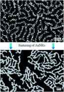
Low temperature sintering of metallic nanoparticles can be used to enhance the thermal properties of composite, thermal interface materials. Here, we present an approach to achieve the coalescence and sintering of a gold nanorod (AuNR) assembly in a block copolymer pattern by thermal annealing at low temperatures. Prior to thermal annealing in a conventional furnace or a rapid thermal processing unit, self-assembly of AuNRs is directed by the guidance of nanochannels in the block copolymer thin films and the removal of surfactants by a brief plasma treatment. Both furnace thermal annealing and rapid thermal annealing are employed to study the sintering behavior of the AuNR assembly. It is found that the sintering process initially takes place locally, resulting in small AuNR aggregates. Eventually the aggregates grow into a globally continuous, percolating network structure. The condensation heat transfer coefficient was measured in an environmental scanning electron microscope by following droplet growth over time and it is shown to be 3.7 times higher for AuNR composites.


1. Introduction

During the past decade, polymer nanocomposites have attracted much attention because of their enhanced optical,1,2 mechanical,3,4 thermal,5–8 and electrical9,10 properties. Various kinds of inorganic nanoparticles, ranging from silver and gold to carbon nanotubes, have been incorporated to improve either thermal or electrical conductivity.7–11 These enhancements are increasingly important in the microelectronics industry since heat dissipation has become a significant problem as the scaling of devices continues. A high loading of thermally or electrically conductive particles that exceeds the percolation threshold, is necessary to achieve a large improvement in the conductivity.12 The connected network structure that exists once the percolation threshold is crossed, provides effective pathways for phonon or electron transport. However, a high volume fraction of inorganic nanoparticles in the polymeric matrix may cause several issues, including reduced flexibility, poor mechanical performance, and dramatically increased viscosity prior to polymer curing. Therefore, great efforts have been made to try to achieve a percolated network without sacrificing other desirable material properties. In our previous work,13 we explored the possibility of using patterned block copolymer thin films to guide the end-to-end self-assembly of gold nanorods and hence to fabricate a continuous network structure within the lamellar pattern. Liu et al. has also achieved ordered two-dimensional gold nanorod arrays via plasma-ashed block copolymer templates.14 Gold nanorods and tellurium nanowires, used as nanoparticle “monomers”, were “polymerized” into long-chain structure following the chain-growth polymerization mode by Wang et al., which offered rational design for complex nanostructures.15 Kim and coworkers studied the correlation between the percolation threshold and the aspect ratio of carbon nanotubes and concluded that the percolation threshold decreased with increasing aspect ratios.16

Many researchers have also investigated approaches to reduce the interfacial resistance between individual nanoparticles and hence to reinforce the connection or bonding strength. Of particular interest has been the sintering process. Melting point depression is a prominent phenomenon in nanoscale materials, which melt at temperatures hundreds of degrees lower than the bulk materials.17 Sintering of these nanoparticles can take place at an even lower temperature due to premelting of the surface atoms.18,19 A variety of techniques, including thermal,7,8,20,21 electrical,22,23 laser,24 microwave,25 plasma,14,26 and electron beam27 methods have been applied to promote the sintering of metal nanoparticles. Surprisingly, the sintering of gold and silver nanoparticles has been demonstrated at room temperature using a simple chemical treatment to remove the surfactants. Since the reaction is exothermic, once the surfactants were removed, the nanoparticles sintered.28,29 While the fusion of isotropic nanoparticles, i.e. nanospheres, has met with great success, there are limited studies30,31 on the sintering behaviour of their anisotropic counterparts, such as nanorods. In many applications, this anisotropy is the origin of some distinct optical,32 physical,33,34 and electrical35,36 properties. It is important to note that most metal nanoparticles are functionalized with an organic capping agent to prevent agglomeration and ensure good dispersion of the nanoparticles in the polymer matrix. However, it is essential to remove these surfactants prior to sintering because they present a high energy barrier for the diffusion of metal atoms. We demonstrated successful use of thermal treatment to detach polyvinylpyrrolidone from silver nanoparticle surface.7,8 Winkler et al. employed oxygen plasma to decompose the organic material on gold nanoparticles.26

There are two primary mechanisms responsible for the sintering process. One is Ostwald ripening, in which individual atoms leave a smaller metal particle and attach to a larger metal particle.37,38 The end result is that large particles grow at the expense of small particles. The other one is attractive migration and coalescence.39,40 In this sintering mechanism, metal particles are either close enough to each other or free to move so that they can collide with other particles, resulting in coalescence. The formation of a neck between adjacent particles is a strong indication of this mechanism.

In this paper, we explored the possibility of achieving a percolating gold network guided by a block copolymer pattern. After deposition of a AuNR dispersion onto the channel patterns, the AuNRs could be directed and sequestered in the block copolymer pattern.13 The AuNR assembly was then thermally annealed at low temperatures ranging from 115 to 200 °C both in a conventional furnace and in a rapid thermal processing unit to sinter the particles and thus form a continuous network nanostructure. The sintering process was initiated by coarsening between neighbouring AuNRs as confirmed by SEM imaging. Further annealing led to a coarse network structure with a small number of isolated AuNRs. Eventually, the migration and integration of individual AuNRs to the main network eliminated isolated particles and the structure was smoothed by surface atom diffusion.

2. Experimental

2.1. Materials

The following chemicals were used as received. Hydrogen tetrachloroaurate trihydrate (HAuCl4·3H2O), hexadecyltrimethylammonium bromide (CTAB, >99.0%), silver nitrate (AgNO3, >99%), sodium borohydride (NaBH4, 99%), 5-bromosalicylic acid (>98.0%), and thiol-terminated polyethylene glycol (PEG-SH) polymers (O-[2-(3-mercaptopropionylamino)ethyl]-O′-methylpolyethylene glycol, Mn = 2000) were purchased from Sigma Aldrich. Polystyrene-block-poly(methyl methacrylate) (SMMA, 95k-b-95k) was obtained from Polymer Source, Inc. Ultrapure water produced by a Milli-Q Integral5 system was used in all experiments.

2.2. Preparation of directed self-assembly of AuNRs in patterned SMMA thin films

AuNRs were synthesized using a seed-mediated approach developed by the Murray group.41 Ligand exchange was performed to replace CTAB with PEG-SH so that the AuNRs could be dispersed in ethanol (see ESI for details). The sample used for the thermal annealing experiments had an average aspect ratio of 3.6 and the mean length of the sample was 38.2 ± 5.4 nm. The SMMA block copolymer patterns were generated by selective removal of poly(methyl-methacrylate) (PMMA) domains using oxygen plasma after SMMA formed lamellar thin films (∼80 nm in thickness) on a silicon substrate. Next, the AuNR dispersion in ethanol was deposited onto a patterned SMMA thin film in a covered Petri dish. Slow solvent evaporation led to controlled assembly of the AuNRs.

2.3. Thermal annealing experiments

Prior to the thermal annealing experiments, the AuNR composite was treated with a 90 W oxygen plasma for 10 s. Then, it was annealed by one of two techniques. In the first method, the annealing was performed in a standard laboratory oven in a dry, nitrogen atmosphere. The samples were heated to the target temperature at a speed of 10 °C min−1 and then held at that temperature for a specified length of time. The samples were cooled at 10 °C min−1 until they reached room temperature. In the second technique, rapid thermal annealing was performed in a Jiplec Jetfirst 100 rapid thermal processor. The temperature of the tool was brought up to target temperatures at a ramp rate of 25 °C s−1 and the dwell time of 1–8 min was used. Then the samples were cooled to room temperature at a rate of 25 °C s−1 using circulating water and inert gas supplies.

2.4. Characterization

Scanning electron microscopy (SEM) images were obtained with a Carl Zeiss Supra SEM operating at 2.0 kV. The condensation of water vapour was performed in a FEI Versa 3D environmental scanning electron microscope (ESEM). The temperature of the samples was controlled by a Peltier cooling stage and the samples were imaged with a gaseous secondary electron detector (GSED). The electron beam energy was set to 10 keV in order to minimize the electron beam heating effects. In the experiment, the temperature of the Peltier cooling stage was held at 1 °C (corresponding to a saturation pressure of 651 Pa) and the chamber pressure was maintained at 660 Pa during imaging. The contact angles of water on the different surfaces were recorded with a Rame-Hart Model 500 Advanced Goniometer.

3. Results and discussion

3.1. Directed self-assembly of gold nanorods in patterned block copolymer thin films

Directed self-assembly of AuNRs was obtained by depositing AuNRs dispersed in ethanol onto patterned block copolymer thin films followed by the slow evaporation of the solvents. The SEM images of polystyrene-block-poly(methyl methacrylate) (SMMA) thin films after selective removal of poly(methyl methacrylate) (PMMA) block via oxygen plasma ashing are presented in Fig. 1a and b, where percolating pathways comprised of PMMA nanochannels are clearly seen. The PMMA regions appear darker than PS domains on the template due to plasma ashing. In our previous work,13 we have shown that evaporation of the solvents leads to formation of a three-phase (vapour-dispersion-substrate) contact line. As the three-phase contact line recedes across the patterned block copolymer thin film, the resultant capillary force drives the movement of the nanorods until they are trapped into the nanochannels. Once the AuNRs are inside the PMMA channels, they are subject to an interface curvature field created by the concave meniscus of the solvents. The curvature-induced field is capable of steering and driving the translation of gold nanoparticles, giving rise to the AuNR ensembles shown in Fig. 1c and d. The majority of AuNRs were confined to the PMMA channels, and they exhibited a preference to align in a parallel configuration with respect to the underlying microdomains. This is advantageous since it facilitates the end-to-end alignment of AuNRs and thus lowers the percolation threshold, which means percolation of the nanoparticles in the block copolymer pattern could be obtained at a lower concentration. It is worth noting that there was a significant amount (∼36% number density) of nanosphere impurities along with AuNRs in the thin films. This is due to the fact that at low aspect ratios, the synthesis leads to a large number of nanosphere by-products. Similar to their nanorod counterparts, gold nanospheres mainly located in the PMMA channels and their presence did not seem to disrupt the percolating assembly. More importantly, sintering could occur between nanospheres and nanorods when thermal energy was applied, as will be discussed later.
image file: c5ra07900d-f1.tif
Fig. 1 SEM images, at two magnifications, of patterned SMMA thin films (a and b) and directed self-assembly of AuNRs (average aspect ratio = 3.6 and mean length of the sample = 38.2 ± 5.4 nm) in the patterned SMMA thin films (c and d). The darker stripes correspond to PMMA domains, in which the AuNRs reside.

3.2. Furnace thermal annealing

While the formation of AuNR assemblies guided by the nanochannels in the patterned block copolymer thin films is crucial, the sequestration of nanorods itself will not be of great use unless the AuNRs are sintered to form continuous pathways and a percolating structure. The AuNRs in all the experiments were protected by a polymer layer, thiol-terminated polyethylene glycol (PEG-SH), so that they would be well-dispersed in the solvent instead of agglomerating. To determine the minimal separation between AuNRs, the thickness of the PEG-SH brush is estimated from the radius of gyration, Rg, using the equation obtained by Devanand and coworkers:42
 
Rg = 0.0215Mw0.583 nm (1)

The molecular weight of the PEG-SH is 2000, resulting in a gyration radius of ∼1.8 nm. Thus, adjacent nanorods are separated by a distance of at least 3.6 nm. This 3.6 nm separation is too far apart for efficient sintering. The large inter-particle distance can be reduced by two routes, either using a PEG-SH with a smaller molecular weight or applying PEG-SH removal. We tried to use PEG-SH with a molecular weight of 800 for the ligand exchange. However, a significant degree of agglomeration of AuNRs was observed from SEM images (not shown), probably due to insufficient protection from short PEG-SH molecules. Thus in this work, the PEG-SH surface coating on AuNRs was removed by applying oxygen plasma for 10 s.

Fig. 2 shows the self-assembled AuNRs in patterned SMMA thin films after furnace thermal annealing (FTA) at 115 °C to 135 °C for different times. When the AuNR ensemble was annealed at 115 °C, they showed no significant difference in size over the first 2 h when compared with those obtained at room temperature. Sintering of the AuNRs due to coalescence between adjacent nanoparticles took place only after 6 h (Fig. 2c).


image file: c5ra07900d-f2.tif
Fig. 2 SEM images of AuNR assemblies in patterned SMMA thin films after furnace thermal annealing at 115 °C (a–d), 125 °C (e–h) and 135 °C (i–l). The samples were annealed for 1 h, 2 h, 6 h and 12 h, respectively, from top to bottom.

This sintering behavior is attributed primarily to the premelting of the gold atoms at the surface of AuNRs. As a result, a liquid layer was formed on a metal core, as shown by Barrat and coworkers using MD simulation.43 Since AuNRs in the assemblies were separated by a very short distance or even in physical contact, the liquid layer on different AuNRs could flow and join one another to form a neck. This is very similar to the morphology of a typical sintering process at the initial stage. No remarkable change of the morphology of the AuNR ensemble was found by further extending the annealing time to 12 h (Fig. 2d). If the annealing temperature was increased to 125 °C, sintering of AuNRs occurred in a shorter time, at 2 h, as is clearly seen in Fig. 2f. However, this sintering behavior was found only locally, where aggregates were composed of at most 3–4 gold nanoparticles. As the annealing progressed, the scope of sintering expanded and more and more AuNRs were joined together until a microscopically continuous gold network with barely any breakage was formed (Fig. 2h). However, individual AuNRs were still present around the network, maintaining their rod shape. At this relatively low temperature, the thickness of the liquid layer on the surface could be very small, and therefore the shape of the nanoparticles was determined by the metal core which remained rod-like in shape. Sintering could be observed even sooner, i.e. in 1 h, when the annealing temperature rose to 135 °C (Fig. 2i). Similar to those annealed at 125 °C, AuNRs started with local sintering, and gradually grew into a network where continuous pathways were accomplished. Moreover, the portion of isolated nanoparticles reduced and the gold networks appeared much smoother than those obtained at 125 °C (Fig. 2l).

The structural and morphological changes for assemblies of AuNR undergoing thermal annealing are quite different from individual AuNRs that have been annealed44 or exposed to laser irradiation.45 For well-distributed AuNRs on a substrate, when they are treated with thermal annealing, the aspect ratio of the nanorods decreases gradually with increasing annealing time up to 2 h and temperature up to 250 °C, and eventually all the rod shaped nanoparticles are transformed into spheres, as evidenced by their time-evolving ultraviolet-visible spectra.44 The maximum temperature examined in that work is much lower than the melting point of the bulk gold, which indicates that the morphological changes stem from surface melting. However, no coalescence of AuNRs due to sintering was seen since they are too far apart to approach one another. Alternatively, when AuNRs are exposed to laser pulses,45 they undergo a different transformation process. Point and planar defects including twins and stacking faults are induced in the as-prepared defect-free AuNRs. In this way the AuNRs convert their less stable facets into more stable facets via surface reconstruction and diffusion to minimize the surface energy.

In the temperature range from 115 °C to 135 °C, sintering among AuNRs in close proximity was evident within 12 h. When the temperature dropped slightly to 100 °C, no sign of sintering could be observed even after annealing for 12 h, as shown in Fig. 3a and b. However, if the annealing temperature was set too high, i.e. 240 °C (Fig. 3c and d), a completely different structure was exhibited. The AuNRs could no longer maintain their rod-like shape, and they transformed to nanospheres instead. At high temperatures, the thickness of the surface melting layer became much larger and perhaps only a small core was not melted. Therefore, to lower the surface energy, the gold atoms would flow and finally reorganized to form spheres. This is very similar to what Petrova et al. observed in their study44 and it reveals the important role of surface melting in the shape transformation. Due to their mobility on the substrate, neighboring particles could further fuse to form a larger sphere, driven by additional reduction in the surface energy. It is important to note that the gold nanoparticles were still well aligned in accordance with the original underlying block copolymer pattern despite the fact that the morphology of the block copolymer degraded at such a high temperature, i.e. 240 °C.


image file: c5ra07900d-f3.tif
Fig. 3 SEM images at two magnifications of AuNR assemblies in patterned SMMA thin films after furnace thermal annealing at 100 °C for 12 h (a and b) and 240 °C (c and d).

3.3. Rapid thermal annealing

Another technique that was applied to obtain sintering of AuNRs was rapid thermal annealing (RTA) in order to reduce the process time. As shown in Fig. 4, coalescence and coarsening between neighboring AuNRs started to take place within just a few minutes. This is due to the much higher power densities in a rapid thermal processing unit than in a conventional furnace. In fact, AuNRs began to sinter within 2 min at 180 °C (Fig. 4b) and within 1 min at 200 °C (Fig. 4e). As the annealing process continued, the grains grew both in width and length by integrating more and more gold nanoparticles, and an extensively continuous network structure was formed in the end, providing direct evidence of coalescence (Fig. 4d and g). The number of isolated gold nanoparticles also decreased probably because they migrated to the main network due to enhanced particle mobility at high temperatures and polymer softening since the working temperature was much higher than the polymer's glass transition temperature (107 °C). In the meantime, the metal stripes comprised of fused AuNRs turned smoother which was caused by surface atom diffusion. This nanostructure was better developed in terms of smoothness and number density of isolated nanoparticles. It is interesting to note that gaps in the range of ∼100 to 300 nm started to appear in the nanostructure during the formation of gold network. The tendency to crack could be attributed to the intrinsic volume reduction46 during the sintering process and weak adhesion between the gold nanoparticles and the polymer films. Despite the fact that the integrity of the network was compromised locally by the cracks and breakages, the nanostructure appeared to remain globally continuous.
image file: c5ra07900d-f4.tif
Fig. 4 SEM images of AuNR assemblies in patterned SMMA thin films after rapid thermal annealing at 180 °C for 1, 2, 4, 8 min (a–d), and 200 °C (for 1, 2, 4 min (e–g), respectively).

3.4. Comparison between FTA and RTA

Both FTA and RTA can serve as effective tools to anneal and eventually sinter AuNRs to form percolating networks. The sintering process was initiated between AuNRs in close proximity. Due to the weak adhesion between AuNRs and the underlying substrate, diffusion of AuNRs can happen so that adjacent nanoparticles come into physical contact with each other. Prior to the complete melting of the nanoparticles, a liquid layer at the surface exists because of premelting of the gold atoms. This is supported by molecular dynamics (MD) simulation performed by Barrat and coworkers.43 The driving force for the coalescence of two AuNRs is the reduction in surface energy since the surface area of the new particle is less than the sum of the surface areas of two original AuNRs. As the annealing temperature rises, it takes less time for the AuNRs to start sintering. At the initial stage of annealing, depending on the orientation of the neighboring AuNRs, the sintering process could be categorized into three types: tip-to-tip, side-by-side, and end-to-end, as shown in Fig. 5. Morphological observation of the SEM micrographs have directly shown these three kinds of sintering processes, as indicated with solid red, dashed green, and dotted blue rectangles, respectively, in Fig. 5a. As presented in Fig. 1d, the AuNRs showed a preference to orient parallel to the underlying block copolymer template, forming the tip-to-tip configuration, especially in linear regions. These AuNRs would sinter in the tip-to-tip fashion. Depending on the ratio between the channel width and the diameter of the AuNR there could be up to 3 AuNRs in a single channel, arranged side by side. These AuNRs would sinter in the second configuration and form a particle with bigger diameter. While in the curved areas, it is necessary for the AuNRs to sinter in an end-to-end way.
image file: c5ra07900d-f5.tif
Fig. 5 SEM image showing the beginning phase of sintering process (a), and schematics of tip-to-tip (b), side-by-side (c), and end-to-end (d) sintering between adjacent AuNRs.

As the thermal annealing continues, locally sintered gold nanoparticles keep growing to form a globally connected structure by merging smaller grains. However, individual AuNRs far away from the metal network would still maintain their rod shape because the solid metal core holds in spite of surface melting. Eventually, these isolated AuNRs are brought closer together, driven by enhanced particle mobility at high temperatures and the softening of underlying polymers, and sinter to become part of the percolating nanostructure. Meanwhile, the atoms of the liquid-like surface layer diffuse and smooth the network to further reduce the system energy. While the mechanism for thermal sintering is similar to both FTA and RTA, there are substantial differences between these two techniques. In FTA, the heat transfer is governed by conduction or convection mechanisms. While in RTA, the high heating rate can be accomplished by high energy radiative sources, typically halogen lamps. Due to the high power density output from the lamp and strong absorption by the gold particles, RTA can be completed in a much shorter time than FTA. This high power density is also beneficial to “heal” the local defects and hence form a well-developed network structure.

3.5. Thermal property measurements with ESEM

Since the thickness of the block copolymer nanocomposites with AuNR assemblies is very small, i.e. less than 100 nm, it is extremely difficult to measure the thermal or electrical conductivity directly. Therefore, water condensation on the surfaces within an environmental scanning electron microscope (ESEM) was employed here to study the thermal properties of the thin film materials. ESEM is a relatively new technique, and it has been widely used to study the growth dynamics and mechanisms of water droplets both on flat surfaces47,48 and complex nanostructures,49,50 due to its enhanced spatial resolution, better control of vapour pressure, and advantage in controlling contamination issues and noncondensable gases. In our experiments, ESEM images were recorded to observe the condensation of water vapour on two surfaces, an annealed block copolymer surface and a gold/polymer composite surface. As displayed in Fig. 6 at the start of data recording, the diameter of the water droplet condensed on the gold composite surface was about 3 times of that on neat SMMA thin film. The droplets on both surfaces grew almost linearly with time. Furthermore, the water droplet growth rate for sintered AuNRs (∼7.3 nm s−1) was larger than that for pristine SMMA thin film (∼2.1 nm s−1) by a factor of ∼3.5. It is known that vapour condensation is an exothermic process. Hence the larger the thermal conductivity of the underlying substrate, the faster the heat released from condensation can be dissipated, and the larger the droplet growth rate. This explains the great enhancement in condensation rate on sintered AuNR nanostructures.
image file: c5ra07900d-f6.tif
Fig. 6 Growth of water droplet on neat SMMA thin film (black square) and sintered AuNRs on SMMA (red circle).

We can use the information on drop growth rate, substrate temperature and system pressure to estimate the mass transfer and heat transfer coefficients for a single drop. To determine the volume of a drop, we assume it is a portion of a sphere and measure the contact angle. The contact angle of water on SMMA thin film and sintered AuNRs on SMMA film were 69.5° and 73.3°, respectively, indicating that both surfaces were hydrophilic. Fig. 7a shows an optical image of the water drop, which could be treated as a spherical cap. The volume of the spherical cap and area of the liquid–vapour interface are given below:51

 
image file: c5ra07900d-t1.tif(2)
 
A = 2πR2(1 − cos[thin space (1/6-em)]θ) (3)
where R is the radius of the sphere, and θ is the contact angle.


image file: c5ra07900d-f7.tif
Fig. 7 (a) Optical image of a sessile water drop on block copolymer thin film. (b) Schematic of a liquid drop on a flat surface.

The ESEM chamber pressure was set at 660 Pa and so we could treat the system as an ideal gas. Hence the mass transfer rate could be expressed in terms of a pressure driving force as:52

 
NA = kp(psat(vap) − psat(surf)) (4)
where NA is the mass transfer rate, kp is the gas-phase mass transfer coefficient, psat(vap) is the saturation pressure of the vapour phase, 660 Pa, and psat(surf) is the saturation pressure of the vapour at the surface temperature, Ts. The Peltier cooling stage in the ESEM was set to 1 °C. Here we assume the temperature of the liquid is the same as that of the substrate, Tl = Ts (Fig. 7b). According to the Antoine equation,53 the relationship between the saturated pressure (in mmHg) and the saturation temperature (in °C) is given by
 
image file: c5ra07900d-t2.tif(5)

For water, the values for the constants A, B, and C are 8.0713, 1730.63, and 233.427, respectively. Therefore, the temperature of the vapour phase, Tsat is calculated to be 1.18 °C and the vapour pressure right above the drop surface, psat(surf) was determined to be 651 Pa. The mass transfer rate based on unit area of the liquid–vapour interface is expressed as:

 
image file: c5ra07900d-t3.tif(6)
where M is the molecular weight of the vapour phase, in our case it is 18 kg kmol−1 for water. Combining eqn (4) and (6), we find that the mass transfer coefficients are 5.50 × 10⁻¹⁰ kmol s kg−1 m−1, and 2.04 × 10⁻⁹ kmol s kg−1 m−1 for the SMMA film and the composite film, respectively.

The corresponding heat transfer rate during the condensation is given by

 
q = hfg = hfgρ[V with combining dot above] (7)

In this equation, hfg is the latent heat of water condensation, 2260 kJ kg−1, and ρ is the density of water, 1000 kg m−3. Hence, the heat flux during condensation is the heat transfer rate per unit area of the liquid–vapour interface

 
image file: c5ra07900d-t4.tif(8)

Meanwhile, the surface heat flux may be expressed as

 
q′′s = h(TsatTs) (9)
where h is the convection heat transfer coefficient, Tsat is the saturation temperature for the water vapour, 1.18 °C. By equating eqn (8) and (9), we can show that the convection heat transfer coefficient for a single drop on a pristine SMMA thin film is 6.71 W m−2 K−1, while that for the composite film is 24.90 W m−2 K−1.

In our system, there are three resistances to transferring heat. The first is getting the vapour molecules to the liquid–vapour interface, the second is converting the vapour to liquid, and the last is removing the heat released during the condensation process. We attribute the difference in heat transfer coefficient to the enhanced ability of the surface to conduct heat away from the drop and maintain the interface at a low temperature. The relatively low heat transfer coefficients overall can be attributed to the low mass transfer rate within the ESEM chamber. The increase in heat transfer coefficient by a factor of 3.7 further proves the improvement in thermal properties of thin films after AuNRs are sintered to form a percolating network nanostructure.

4. Conclusions

In summary, we have demonstrated that gold nanorods can be sintered with thermal annealing after they are selectively sequestered in block copolymer patterns to form a continuous network structure and align in an end-to-end fashion. Both furnace thermal annealing and rapid thermal annealing are explored to study the sintering behaviour of gold nanorods. It has been found that the development of well-defined percolating metal network consists of three phases. In the beginning, gold nanorods in close proximity coalesce with each other in a tip-to-tip, side-by-side or end-to-end manner, which is facilitated by surface premelting and driven by the reduction in surface energy. Then the scope of sintering spreads across the thin film, leading to globally connected gold networks. Finally, individual gold nanorods away from the main frame adhere to the network and smooth gold lines are accomplished. Rapid thermal annealing is advantageous over furnace thermal annealing not only because the processing time is shorter but also because of its capability for better development of percolating gold network due to high power intensity. The condensation of water vapour on sintered AuNR nanostructures is ∼3.5 times faster than that on SMMA thin film, resulting in a 3.7× increase in convection heat transfer coefficient, which indicates the improved thermal conductivity of the materials. These results open up new possibilities in the development of percolating pathways for improvement in thermal and electrical properties.

Acknowledgements

This work is supported by both IBM and NSF under contract #ECCS-1127731.

References

  1. G. Q. Jiang, M. J. A. Hore, S. Gam and R. J. Composto, ACS Nano, 2012, 6, 1578–1588 CrossRef CAS PubMed.
  2. G. Q. Jiang, A. Baba, H. Ikarashi, R. S. Xu, J. Locklin, K. R. Kashif, K. Shinbo, K. Kato, F. Kaneko and R. Advincula, J. Phys. Chem. C, 2007, 111, 18687–18694 CAS.
  3. M. Moniruzzaman and K. I. Winey, Macromolecules, 2006, 39, 5194–5205 CrossRef CAS.
  4. T. Ramanathan, A. A. Abdala, S. Stankovich, D. A. Dikin, M. Herrera-Alonso, R. D. Piner, D. H. Adamson, H. C. Schniepp, X. Chen, R. S. Ruoff, S. T. Nguyen, I. A. Aksay, R. K. Prud'homme and L. C. Brinson, Nat. Nanotechnol., 2008, 3, 327–331 CrossRef CAS PubMed.
  5. P. Meneghetti and S. Qutubuddin, Thermochim. Acta, 2006, 442, 74–77 CrossRef CAS PubMed.
  6. W. L. Song, W. Wang, L. M. Veca, C. Y. Kong, M. S. Cao, P. Wang, M. J. Meziani, H. J. Qian, G. E. LeCroy, L. Cao and Y. P. Sun, J. Mater. Chem., 2012, 22, 17133–17139 RSC.
  7. K. Pashayi, H. R. Fard, F. Lai, S. Iruvanti, J. Plawsky and T. Borca-Tasciuc, J. Appl. Phys., 2012, 111, 104310 CrossRef PubMed.
  8. K. Pashayi, H. R. Fard, F. Y. Lai, S. Iruvanti, J. Plawsky and T. Borca-Tasciuc, Nanoscale, 2014, 6, 4292–4296 RSC.
  9. X. M. Zeng, X. F. Xu, P. M. Shenai, E. Kovalev, C. Baudot, N. Mathews and Y. Zhao, J. Phys. Chem. C, 2011, 115, 21685–21690 CAS.
  10. A. V. Kyrylyuk, M. C. Hermant, T. Schilling, B. Klumperman, C. E. Koning and P. van der Schoot, Nat. Nanotechnol., 2011, 6, 364–369 CrossRef CAS PubMed.
  11. J. W. Chung, S. W. Ko, N. R. Bieri, C. P. Grigoropoulos and D. Poulikakos, Appl. Phys. Lett., 2004, 84, 801–803 CrossRef CAS PubMed.
  12. A. V. Kyrylyuk and P. van der Schoot, Proc. Natl. Acad. Sci. U. S. A., 2008, 105, 8221–8226 CrossRef CAS PubMed.
  13. F. Lai, T. Borca-Tasciuc and J. Plawsky, Nanotechnology, 2015, 26, 055301 CrossRef PubMed.
  14. Z. Liu, H. Huang and T. He, Small, 2013, 9, 505–510 CrossRef CAS PubMed.
  15. H. Wang, X. H. Song, C. C. Liu, J. T. He, W. H. Chong and H. Y. Chen, ACS Nano, 2014, 8, 8063–8073 CrossRef CAS PubMed.
  16. J. Li, P. C. Ma, W. S. Chow, C. K. To, B. Z. Tang and J. K. Kim, Adv. Funct. Mater., 2007, 17, 3207–3215 CrossRef CAS PubMed.
  17. P. Buffat and J.-P. Borel, Phys. Rev. A, 1976, 13, 2287–2298 CrossRef CAS.
  18. J. W. M. Frenken and J. F. Vanderveen, Phys. Rev. Lett., 1985, 54, 134–137 CrossRef CAS.
  19. K. S. Moon, H. Dong, R. Maric, S. Pothukuchi, A. Hunt, Y. Li and C. P. Wong, J. Electron. Mater., 2005, 34, 168–175 CrossRef CAS.
  20. H. Pan, S. H. Ko and C. P. Grigoropoulos, Appl. Phys. Lett., 2008, 93, 234104 CrossRef PubMed.
  21. B. T. Anto, S. Sivaramakrishnan, L. L. Chua and P. K. H. Ho, Adv. Funct. Mater., 2010, 20, 296–303 CrossRef CAS PubMed.
  22. M. L. Allen, M. Aronniemi, T. Mattila, A. Alastalo, K. Ojanpera, M. Suhonen and H. Seppa, Nanotechnology, 2008, 19, 175201 CrossRef PubMed.
  23. M. Hummelgard, R. Y. Zhang, H. E. Nilsson and H. Olin, PLoS One, 2011, 6, e17209 Search PubMed.
  24. S. H. Ko, H. Pan, C. P. Grigoropoulos, C. K. Luscombe, J. M. J. Frechet and D. Poulikakos, Appl. Phys. Lett., 2007, 90, 141103 CrossRef PubMed.
  25. J. Perelaer, B. J. de Gans and U. S. Schubert, Adv. Mater., 2006, 18, 2101–2104 CrossRef CAS PubMed.
  26. K. Winkler, T. Wojciechowski, M. Liszewska, E. Gorecka and M. Fialkowski, RSC Adv., 2014, 4, 12729–12736 RSC.
  27. Y. Chen, R. E. Palmer and J. P. Wilcoxon, Langmuir, 2006, 22, 2851–2855 CrossRef CAS PubMed.
  28. M. J. Coutts, M. B. Cortie, M. J. Ford and A. M. McDonagh, J. Phys. Chem. C, 2009, 113, 1325–1328 CAS.
  29. S. Magdassi, M. Grouchko, O. Berezin and A. Kamyshny, ACS Nano, 2010, 4, 1943–1948 CrossRef CAS PubMed.
  30. B. Q. Sun, R. L. Peterson, H. Sirringhaus and K. Mori, J. Phys. Chem. C, 2007, 111, 18831–18835 CAS.
  31. B. Mukherjee, B. Viswanath and N. Ravishankar, J. Phys. D: Appl. Phys., 2010, 43, 455301 CrossRef.
  32. T. Chen, H. Wang, G. Chen, Y. Wang, Y. H. Feng, W. S. Teo, T. Wu and H. Y. Chen, ACS Nano, 2010, 4, 3087–3094 CrossRef CAS PubMed.
  33. W. U. Huynh, J. J. Dittmer and A. P. Alivisatos, Science, 2002, 295, 2425–2427 CrossRef CAS PubMed.
  34. M. A. Modestino, E. R. Chan, A. Hexemer, J. J. Urban and R. A. Segalman, Macromolecules, 2011, 44, 7364–7371 CrossRef CAS.
  35. S. I. White, B. A. DiDonna, M. F. Mu, T. C. Lubensky and K. I. Winey, Phys. Rev. B: Condens. Matter Mater. Phys., 2009, 79, 021301 Search PubMed.
  36. R. M. Mutiso, M. C. Sherrott, A. R. Rathmell, B. J. Wiley and K. I. Winey, ACS Nano, 2013, 7, 7654–7663 CrossRef CAS PubMed.
  37. P. W. Voorhees, J. Stat. Phys., 1985, 38, 231–252 CrossRef.
  38. C. T. Campbell, S. C. Parker and D. E. Starr, Science, 2002, 298, 811–814 CrossRef CAS PubMed.
  39. W. C. Yang, M. Zeman, H. Ade and R. J. Nemanich, Phys. Rev. Lett., 2003, 90, 136102 CrossRef CAS.
  40. S. Liang, H. L. Zhu, D. H. Kong and W. Wang, J. Appl. Phys., 2010, 108, 073512 CrossRef PubMed.
  41. R. A. Farrell, N. T. Kinahan, S. Hansel, K. O. Stuen, N. Petkov, M. T. Shaw, L. E. West, V. Djara, R. J. Dunne, O. G. Varona, P. G. Gleeson, S. J. Jung, H. Y. Kim, M. M. Kolesnik, T. Lutz, C. P. Murray, J. D. Holmes, P. F. Nealey, G. S. Duesberg, V. Krstic and M. A. Morris, Nanoscale, 2012, 4, 3228–3236 RSC.
  42. K. Devanand and J. C. Selser, Macromolecules, 1991, 24, 5943–5947 CrossRef CAS.
  43. L. J. Lewis, P. Jensen and J. L. Barrat, Phys. Rev. B: Condens. Matter Mater. Phys., 1997, 56, 2248–2257 CrossRef CAS.
  44. H. Petrova, J. P. Juste, I. Pastoriza-Santos, G. V. Hartland, L. M. Liz-Marzan and P. Mulvaney, Phys. Chem. Chem. Phys., 2006, 8, 814–821 RSC.
  45. S. Link, Z. L. Wang and M. A. El-Sayed, J. Phys. Chem. B, 2000, 104, 7867–7870 CrossRef CAS.
  46. S. Sivaramakrishnan, P. J. Chia, Y. C. Yeo, L. L. Chua and P. K. H. Ho, Nat. Mater., 2007, 6, 149–155 CrossRef CAS PubMed.
  47. S. Anand and S. Y. Son, Langmuir, 2010, 26, 17100–17110 CrossRef CAS PubMed.
  48. A. Lauri, I. Riipinen, J. A. Ketoja, H. Vehkamaki and M. Kulmala, Langmuir, 2006, 22, 10061–10065 CrossRef CAS PubMed.
  49. K. Rykaczewski and J. H. J. Scott, ACS Nano, 2011, 5, 5962–5968 CrossRef CAS PubMed.
  50. X. M. Chen, J. Wu, R. Y. Ma, M. Hua, N. Koratkar, S. H. Yao and Z. K. Wang, Adv. Funct. Mater., 2011, 21, 4617–4623 CrossRef CAS PubMed.
  51. V. P. Carey, Liquid Vapor Phase Change Phenomena: An Introduction to the Thermophysics of Vaporization and Condensation Processes in Heat Transfer Equipment, Taylor and Francis, New York, 2nd edn, 2008 Search PubMed.
  52. J. D. Seader, E. J. Henley and D. K. Roper, Separation Process Principles: Chemical and Biochemical Operations, Wiley, 2010 Search PubMed.
  53. G. W. Thomson, Chem. Rev., 1946, 38, 1–39 CrossRef CAS.

Footnote

Electronic supplementary information (ESI) available. See DOI: 10.1039/c5ra07900d

This journal is © The Royal Society of Chemistry 2015
Click here to see how this site uses Cookies. View our privacy policy here.