
 Open Access Article
 This Open Access Article is licensed under a
 Creative Commons Attribution 3.0 Unported Licence
Control of carrier mobilities for performance enhancement of anthracene-based polymer solar cells†
Özlem
Usluer
a,
Sameh
Boudiba
bc,
Daniel A. M.
Egbe
b,
Lionel
Hirsch
d and
Mamatimin
Abbas
*d
aDepartment of Energy Systems Engineering, Konya Necmettin Erbakan University, 42090, Meram, Konya, Turkey
bLinz Institute for Organic Solar Cells, Johannes Kepler University, 4040 Linz, Austria
cLaboratoire des Matériaux Organiques et Hétérochimie, Université de Tébessa, Algeria
dCNRS UMR5218, Université Bordeaux, Laboratoire de l’Intégration du Matériau au Système (IMS), 33607 Pessac Cedex, France. E-mail: mamatimin.abbas@ims-bordeaux.fr; Tel: +33 54000 3675
First published on 21st May 2015
Abstract
High performance organic solar cells were realized using an anthracene-based polymer. Charge carrier mobilities of both electrons and holes in solvent annealed polymer and fullerene derivative mixtures were studied using organic field-effect transistors. Fine tuning of donor to acceptor ratios revealed optimum conditions for balanced mobilities, which led to a high power conversion efficiency (PCE) of 4.02% in the organic solar cells. A methanol wash approach further enhanced the PCE to 4.65%. This work demonstrates the importance of carrier transport control in optimizing the performance of polymer solar cells.
Although polymer solar cells have a number of advantages over silicon based solar cells in terms of their low cost, light weight and flexibility etc., one of the bottlenecks to their application is their relatively low power conversion efficiencies (PCEs). Recent advances in chemical and device engineering have pushed PCEs of polymer solar cells over 10%.1 However, for market applications, the PCE has to be further improved. The development of new materials and their integration into efficient device configurations have to be explored. One of the approaches is to fabricate tandem solar cells. Indeed, until now, the highest PCE reported for polymer solar cells was obtained using a tandem structure.2 In this configuration, two or more cells are stacked in series, thus the device open circuit voltage (Voc) will be the sum of Voc achieved from each sub-cell. The absorption profile of the sub-cells should be complimentary in order to achieve the maximum possible short circuit current density (Jsc) from each sub-cell. Recently, identical active layers comprised of low band gap polymer were proposed with quite thin films.3 However, for a large scale process at an industrial level thicker films are preferred due to the requirements of homogeneity and robustness for high production yield. Therefore, both low and wider band gap polymers should be incorporated into tandem solar cells in each sub-cell, in this case, wider band gap polymers that yield high Voc are most useful. One such promising polymer is the anthracene-based PPV polymer. It has an optical band gap of about 2 eV, with a high oxidation potential, resulting in a generally high Voc in polymer solar cells when combined with [6,6]-phenyl-C61-butyric acid methyl ester (PCBM, classical).4 Several studies have been carried out to optimize device performance. Side chain variation has been shown to have a rather strong impact on the pi–pi stacking ability of the polymer backbone, and consequently on device performance. A PCE of 3.03% was achieved for the polymer with optimum side chain distribution, named AnE-PVstat.5 Fine tuning of macromolecular parameters such as molecular weight and polydispersity resulted in a PCE of 3.26%.6 Through the control of blend morphology, by solution concentration and PCBM weight fraction, a high PCE of 4.33% was recently achieved.7 Applying different fullerene derivatives as acceptors has been proposed, and significant variation in PCE was observed.8 A high PCE of 4.3% was achieved when specific fullerene derivatives were applied, compared to 2.9% from classical PCBM.9 Until now, the highest reported PCE based on this polymer was 4.8%, again reached with specific fullerene derivatives.10 In this work, we demonstrate that comparable efficiency can be achieved using classical PCBM when carrier mobilities are controlled. With this aim, we first looked at electron and hole charge transport behavior in the bulk heterojunction films. We started with the donor to acceptor ratio generally used in the literature, then fine-tuned the ratio towards that where balanced mobilities could be observed. A PCE of over 4% was obtained. Methanol washing of the films gave a 4.65% PCE, the highest reported so far for this promising polymer when classical PCBM is used as the acceptor.
The synthesis of the polymer, AnE-PVstat has been described elsewhere.11 PCBM was purchased from Solaris (>99.5%). Molecular structures are given in Fig. 1(a) and (b). To fabricate the bottom gate, top-contact organic field-effect transistor (OFET) devices, a heavily doped Si substrate with thermally grown SiO2 (200 nm) was used as the gate and dielectric. Water soluble poly(1-vinyl-1,2,4-triazole) (PVT) was used as the passivation layer.12–14 PVT was dissolved in high resistivity ultrapure water in a weight ratio of 3%. The solution was filtered and spin-coated (2000 rpm for 60 s) onto SiO2. The films were dried in a vacuum oven for two hours at 80 °C. AnE-PVstat and PCBM were mixed in different weight ratios and dissolved in 1,2-dichlorobenzene with a polymer concentration of 10 mg mL−1 and spin-coated (1000 rpm for 20 s) directly on top of PVT in a dry nitrogen glove box. Spin coated films were slowly dried in Petri dishes over two hours. As source/drain contacts, Au for p-channel operation and Al for n-channel operation were evaporated thermally through a shadow mask to complete the OFET devices. The channel length was 0.05 mm and the channel width was 1 mm. I–V characterizations were performed using a Keithley 4200 semiconductor analyzer in a dry nitrogen glove box. For solar cell device preparation, etched ITO glass substrates with a sheet resistance of 10 Ω sq−1 were used. After cleaning in an ultrasonic bath with acetone, ethanol, and iso-propanol for 15 min and treatment in a UV/O3 cleaner for 20 min, PEDOT:PSS was spin coated at a spin speed of 4000 rpm for 40 s forming 20 nm thick layers and annealed for 30 min at 110 °C. The same solutions and deposition method were used as those for the OFET devices. The thickness of the active layer was about 170 nm. Finally, the Al cathode (100 nm) was thermally evaporated under high vacuum (10−6 mbar) through a shadow mask determining the active surface area of 10 mm2. Current–voltage (I–V) curves were recorded using a Keithley 2400 semiconductor analyzer under illumination of an AM1.5 solar simulator set at 100 mW cm−2, which was calibrated using an IL1400BL radiometer. Samples were measured in a dry nitrogen glove box.
 | ||
| Fig. 1 Molecular structure of AnE-PVstat (a), octyl and 2-ethylhexyl side chains are randomly distributed; molecular structure of PCBM (b); device structure of OFETs (c); device structure of OPVs (d). | ||
In an earlier study we used OFETs to deduce charge carrier behavior in OPVs in the P3HT/PCBM system, where balanced mobilities in the OFETs correlated well with the drastic enhancement in device performance parameters in polymer solar cells.15 For this, a suitable dielectric with a low trap density for both electrons and holes should be employed. Proper source/drain contacts should be used for efficient injection of both charges. Furthermore, all the device related parameters have to be taken into account for deriving reliable mobility values. Thus, we first fabricated OFET devices with a bulk heterojunction as the active layer. Fig. 2 shows the transfer characteristics of the OFET devices for n-channel and p-channel operations. We chose 1![[thin space (1/6-em)]](https://www.rsc.org/images/entities/char_2009.gif) :2 as the starting ratio, as it has been generally used in previous studies as the optimum ratio for the AnE-PVstat polymer.5,9 We observed a much higher electron current compared to the hole current in OFET devices for this ratio. Thus, we finely tuned the polymer to PCBM ratio, in order to reach a similar current for electrons and holes. The ratio of polymer to PCBM was varied between 1:2 to 1:1, i.e. decreasing the relative amount of PCBM in the mixture of the bulk heterojunction film. A notable observation was made when the polymer fraction increased from 33% (1:2) to 50% (1:1): the hole current did not change much, while the electron current decreased by more than one order of magnitude, which indicated percolation of the polymer phase was not strongly affected due to its bulky nature.
:2 as the starting ratio, as it has been generally used in previous studies as the optimum ratio for the AnE-PVstat polymer.5,9 We observed a much higher electron current compared to the hole current in OFET devices for this ratio. Thus, we finely tuned the polymer to PCBM ratio, in order to reach a similar current for electrons and holes. The ratio of polymer to PCBM was varied between 1:2 to 1:1, i.e. decreasing the relative amount of PCBM in the mixture of the bulk heterojunction film. A notable observation was made when the polymer fraction increased from 33% (1:2) to 50% (1:1): the hole current did not change much, while the electron current decreased by more than one order of magnitude, which indicated percolation of the polymer phase was not strongly affected due to its bulky nature.
 | ||
| Fig. 2 Transfer characteristics of the OFET devices at a drain voltage of −10 V for p-channel devices and 10 V for n-channel devices. Donor to acceptor ratios were varied between 1:2 to 1:1. Au source/drain contacts were used for p-channel devices and Al source/drain contacts were used for n-channel devices. | ||
We derived the respective mobilities of electrons and holes in this system using the gradual channel approximation. In a disordered system, charge carrier mobility is strongly dependent on carrier concentration, i.e. the mobility is gate voltage dependent in an OFET device.16 Gate voltage dependent carrier mobility in the saturation regime is given by the formula below:
 | (1) |
In order to obtain reliable mobility values from OFET devices, device related parameters have to be taken into account. One of them is the threshold voltage. The square root of the drain current versus the gate voltage of the saturation curve can be linearly extended to zero current to determine the threshold voltage. Threshold voltage is dependent on several factors, such as the carrier injection barrier between the source contact and the semiconducting active layer, total trap densities (including dielectric and semiconductor bulk, dielectric/semiconductor interface trap densities), interface dipole and dielectric capacitance. Therefore, in an OFET device, most of the device related parameters are accounted for by the threshold voltage. Contact resistance is another factor to be considered that gives underestimated mobilities at higher gate voltages.5 Taking into account these considerations, effective gate voltage Vgs − Vth dependent mobilities of electrons and holes are given in Fig. 3.
 | ||
| Fig. 3 Upper panel: electron and hole mobilities in the saturation regime for different AnE-PVstat to PCBM ratios derived from OFET devices. Lower panel: mobility values obtained at Vgs − Vth = ±3 V. Six devices were tested for each condition. | ||
As is manifest in the hole and electron currents in the transfer curves, the hole mobilities remained mainly constant for the donor to acceptor ratio change within the considered range, while the responses of the electron mobilities were rather drastic. Both gate voltage dependent mobility curves reached a maximum and started to decrease when the gate voltage further increased, a clear effect of contact resistance. Therefore, avoiding this range of data values, we have chosen mobility values at ±3 V for quantitative comparison, shown in lower panel of Fig. 3.
When the polymer to acceptor ratio was 1:2, electron mobility was almost ten times higher than hole mobility. Electron mobility started to drastically decrease until the ratio of 1.2:1.8 was reached. When the acceptor content further reduced to 53% (polymer to acceptor ratio of 1.4:1.6), we observed that hole mobility became higher than electron mobility.
We fabricated polymer solar cells with the same active layer processing condition as that in the OFETs. J–V curves of the devices tested under 100 mW cm−2 AM 1.5 G illumination for different AnE-PVstat to PCBM ratios are shown in the left panel of Fig. 4, and device performance parameters are given in Table 1.
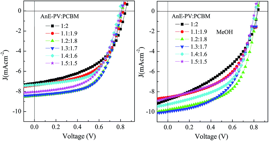 | ||
| Fig. 4 Left panel: J–V curves of solar cell devices tested under 100 mW cm−2 AM 1.5 G illumination for different AnE-PVstat to PCBM ratios. Right panel: J–V curves of the devices where the active layers were treated with methanol. | ||
| AnE-PVstat:PCBM |
J SC (mA cm−2) | V OC (V) | FF (%) | η (%) | R s (Ω) | R sh (Ω) |
|---|---|---|---|---|---|---|
| 1:2 |
7.19 (8.79) | 0.84 (0.84) | 51 (43) | 3.06 (3.14) | 25 (18) | 680 (271) |
| 1.1:1.9 |
7.38 (8.56) | 0.82 (0.82) | 55 (52) | 3.35 (3.61) | 26 (19) | 740 (623) |
| 1.2:1.8 |
8.45 (9.81) | 0.82 (0.84) | 57 (56) | 3.98 (4.65) | 23 (15) | 1079 (515) |
| 1.3:1.7 |
8.37 (9.98) | 0.80 (0.82) | 60 (52) | 4.02 (4.27) | 22 (21) | 1323(674) |
| 1.4:1.6 |
7.35 (9.25) | 0.80 (0.82) | 59 (53) | 3.46 (4.05) | 22 (19) | 1072 (426) |
| 1.5:1.5 |
8.05 (8.63) | 0.80 (0.80) | 55 (53) | 3.56 (3.69) | 29 (19) | 1092 (373) |
The general trend in device performance was quite clear. When the polymer to PCBM ratio was 1:2, we obtained a JSC of 7.19 mA cm−2 and a fill factor of only 51% which consequently yielded the lowest PCE of 3.06%. We attribute this to the large difference (almost ten times) between the mobilities of the holes and electrons as shown in the OFET device mobilities. When charge carrier mobilities are highly unbalanced, built up space charges can be detrimental to charge carrier extraction, which results in a low current density and fill factor. Both JSC and the fill factor were greatly enhanced to 8.37 mA cm−2 and 60%, respectively, for devices with the polymer to PCBM ratio of 1.3:1.7, where electron mobility decreased to be only slightly higher than hole mobility. We achieved a PCE of 4.02% for this device. When the PCBM content was further reduced, the JSC and fill factor started to decrease again. In these cases, we observed lower electron mobilities compared to hole mobilities. One can argue, though, that the difference in electron and hole mobilities is comparable for polymer to PCBM ratios of 1.3:1.7 and 1.5:1.5, as only in the former case is electron mobility slightly higher than hole mobility whereas in the latter case it is vice versa. This can be explained by the differences in the distance for charge carrier collection in thick active layer devices. As has been reported, charge carrier generation in OPVs is mainly limited to the region close to the transparent electrode.17 Therefore, in a conventional device architecture with a thick active layer, electrons have to travel for a longer distance, compared to holes, to be collected. In our case, the active layers were solvent annealed with a thickness of about 170 nm. Hence, a slightly higher electron mobility than hole mobility is favorable for efficient collection of both charges at respective electrodes.
Finally, a methanol wash treatment on the active layer was carried out to further enhance the device performances, as reported in earlier studies for various donor–acceptor systems.18,19 Here we observed that, in all the devices, short circuit current density increased in-line with the decrease in the series resistance. Although fill factors were compensated in accordance with the decreasing trend in shunt resistance, overall the PCE improved in all the devices. The maximum PCE achieved was 4.65% with a JSC of 9.81 mA cm−2 and fill factor of 56%. Passivation of surface trap states has been proposed as the possible mechanism behind the effect of methanol wash on device performance in PTB7/PCBM system.19 Decreased series resistance as well as enhancement in hole mobility towards more balanced electron/hole mobilities have also been suggested. In our study, we did not see an observable difference in both electron and hole mobilities before and after methanol treatment, except at higher gate voltages where the contact resistance effect is pronounced. This is in agreement with the decrease in series resistance in OPV devices after a methanol wash, and comes from enhanced surface charge densities due the passivation of surface trap states.
In summary, we proposed a rational approach to optimize the device performance of a promising anthracene-based polymer. We realized a solar cell device with the highest power conversion efficiency reported for this polymer using classical PCBM as the acceptor. Firstly, we investigated charge carrier mobilities of both electrons and holes in donor/acceptor bulk heterojunction layers using OFETs. We observed almost ten times higher electron mobility than hole mobility for the polymer to PCBM ratio of 1:2, as generally used in the literature. Based on this result, we fine tuned the ratio by reducing the amount of PCBM in the mixture aiming to reach the range where holes and electrons had comparable mobilities. Indeed, we achieved the highest PCE of over 4% at a ratio of 1.3:1.7, where electron mobility was only slightly higher than hole mobility. The methanol wash approach further enhanced cell performances in all the devices leading to decreased series resistance and consequently to increased JSC. The highest PCE of 4.65% was achieved. We consolidated the finding that OFETs are useful in examining charge carrier mobilities in a bulk heterojunction system, providing guidelines towards the optimum ratio of balanced mobilities. We conclude that depending on the device configuration (conventional or inverted) and film thickness, slightly unbalanced charge carrier mobilities may lead to best performance of solar cell devices. Finally, surface treatments (such as methanol wash) can be applied to further push for higher performance.
Acknowledgements
D. A. M. Egbe is grateful to the DFG for financial support in the frame of the priority program SPP1355. He also acknowledges the financial support of FWF through the project Nr: I1703-N20. S. Boudiba acknowledges the financial support of the ICTP, Trieste, Italy, in the frame of the African Network for Solar Energy (ANSOLE) ANEX program.References
- Y. Liu, J. Zhao, Z. Li, C. Mu, W. Ma, H. Hu, K. Jiang, H. Lin, H. Ade and H. Yan, Nat. Commun., 2014, 5, 1–8 Search PubMed.
- A. R. b. M. Yusoff, D. Kim, H. P. Kim, F. K. Shneider, W. J. da Silva and J. Jang, Energy Environ. Sci., 2015, 8, 303–316 CAS.
- J. You, C.-C. Chen, Z. Hong, K. Yoshimura, K. Ohya, R. Xu, S. Ye, J. Gao, G. Li and Y. Yang, Adv. Mater., 2013, 25, 3973–3978 CrossRef CAS PubMed.
- D. K. Susarova, E. A. Khakina, P. a. Troshin, A. E. Goryachev, N. S. Sariciftci, V. F. Razumov and D. A. M. Egbe, J. Mater. Chem., 2011, 21, 2356 RSC.
- O. Usluer, C. Kästner, M. Abbas, C. Ulbricht, V. Cimrova, A. Wild, E. Birckner, N. Tekin, N. S. Sariciftci, H. Hoppe, S. Rathgeber and D. A. M. Egbe, J. Polym. Sci., Part A: Polym. Chem., 2012, 50, 3425–3436 CrossRef CAS PubMed.
- F. Tinti, F. K. Sabir, M. Gazzano, S. Righi, C. Ulbricht, O. Usluer, V. Pokorna, V. Cimrova, T. Yohannes, D. A. M. Egbe and N. Camaioni, RSC Adv., 2013, 3, 6972 RSC.
- C. Kästner, D. A. M. Egbe and H. Hoppe, J. Mater. Chem. A, 2015, 3, 395–403 Search PubMed.
- C. Kästner, D. K. Susarova, R. Jadhav, C. Ulbricht, D. A. M. Egbe, S. Rathgeber, P. A. Troshin and H. Hoppe, J. Mater. Chem., 2012, 22, 15987 RSC.
- P. A. Troshin, O. A. Mukhacheva, O. Usluer, A. E. Goryachev, A. V. Akkuratov, D. K. Susarova, N. N. Dremova, S. Rathgeber, N. S. Sariciftci, V. F. Razumov and D. A. M. Egbe, Adv. Energy Mater., 2013, 3, 161–166 CrossRef CAS PubMed.
- C. Kästner, C. Ulbricht, D. A. M. Egbe and H. Hoppe, J. Polym. Sci., Part B: Polym. Phys., 2012, 50, 1562–1566 CrossRef PubMed.
- D. A. M. Egbe, G. Adam, A. Pivrikas, A. M. Ramil, E. Birckner, V. Cimrova, H. Hoppe and N. S. Sariciftci, J. Mater. Chem., 2010, 20, 9726 RSC.
- M. Abbas, G. Cakmak, N. Tekin, A. Kara, H. Y. Guney, E. Arici and N. S. Sariciftci, Org. Electron., 2011, 12, 497–503 CrossRef CAS PubMed.
- M. Abbas, A. Pivrikas, E. Arici, N. Tekin, M. Ullah, H. Sitter and N. S. Sariciftci, J. Phys. D: Appl. Phys., 2013, 46, 495105 CrossRef.
- D. Thuau, M. Abbas, S. Chambon, P. Tardy, G. Wantz, P. Poulin, L. Hirsch, I. Dufour and C. Ayela, Org. Electron., 2014, 15, 3096–3100 CrossRef CAS PubMed.
- M. Abbas and N. Tekin, Appl. Phys. Lett., 2012, 101, 073302 CrossRef PubMed.
- H. Klauk, Chem. Soc. Rev., 2010, 39, 2643–2666 RSC.
- J. D. Kotlarki and P. W. M. Blom, Appl. Phys. Lett., 2012, 100, 4–6 Search PubMed.
- H. Li, H. Tang, L. Li, W. Xu, X. Zhao and X. Yang, J. Mater. Chem., 2011, 21, 6563 RSC.
- H. Zhou, Y. Zhang, J. Seifter, S. D. Collins, C. Luo, G. C. Bazan, T.-Q. Nguyen and A. J. Heeger, Adv. Mater., 2013, 25, 1646–1652 CrossRef CAS PubMed.
Footnote |
| † Electronic supplementary information (ESI) available. See DOI: 10.1039/c5ra07792c |
| This journal is © The Royal Society of Chemistry 2015 |