P. Motamedi* and
K. Cadien*
Department of Chemical and Materials Engineering, University of Alberta, Edmonton, Alberta, Canada T6G 2V4. E-mail: p.motamedi@ualberta.ca; kcadien@ualberta.ca
First published on 25th June 2015
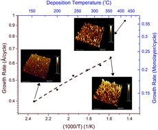
Gallium nitride films were deposited via plasma-enhanced atomic layer deposition (PEALD) using triethylgallium and forming gas as precursors. An optimized process was developed and the effect of growth temperature on the structure and optical properties of the films investigated. In-depth X-ray diffraction analyses show that there is a critical temperature, below which the films are amorphous. Raising the growth temperature above the critical temperature increases the grain size of the polycrystalline film, while degrading the degree of preferred orientation. Azimuthal XRD scans show clear signs of a crystallographic relationship between the (002) planes of the sapphire substrate and GaN. Growth rate shows a steady rise until a rapid jump at 425 °C occurs. The study of the surface profile by AFM shows that the hillocks on the surface start to grow in diameter as well as height, increasing the total growth front area. This also decreases the surface roughness. XRR studies reveal that mass density reaches its maximum value at 240 °C, and is stable after that. Carrier mobility is increased by two orders of magnitude, when the growth temperature is raised from 150 °C to 425 °C. As expected, a similar but reverse trend was observed for the electrical resistivity. Refractive index follows the trends of mass density and crystal quality with a clear increase at the onset of crystallinity. Overall, the surface profile and the engineering properties improve as growth temperature is increased. At the high end of the growth temperature range, PEALD GaN films grown on (002) sapphire were p-type with a hole mobility of 575 cm2 V−1 s−1.
GaN has been grown by metal–organic chemical vapor deposition,1–3 reactive sputtering,4,5 molecular beam epitaxy,6,7 and pulsed laser deposition.8,9 However, there does not appear to be a well-researched method capable of producing crystalline GaN thin films with preferential orientation at low growth temperatures. Atomic layer deposition (ALD) offers exceptional control over the film thickness, conformality, scale-up potential, and considerably lower deposition temperatures.10,11 There are several studies on the effect of growth temperature on the properties of ALD films.12–18 A survey of this literature shows that even when the chemical reactions of the deposition and the physical structure of the films are similar, changing the growth temperature can lead to diverse and even contrasting results. The results of the initial research on the ALD of GaN has been recently published.19–21 However, to date, there is no report on a comprehensive study of the effect of substrate temperature on the growth mechanism, structural evolution, and electrical properties of GaN grown on sapphire.
This paper reports on the effect of substrate temperature on the plasma-enhanced ALD (PEALD) growth mechanism, structural evolution, and electrical properties of GaN, and paves the way for engineering GaN thin films with targeted properties. A comprehensive analysis of the crystal structure, variations of the growth rate and a possible relationship with the changes of the surface roughness is presented. The effect of these structural changes on electrical resistivity, carrier mobility and refractive index of the films are discussed.
The growth rate and film thickness were collected from in situ spectroscopic ellipsometry data. In order to isolate the effect of temperature on the complex dielectric function, total film thickness was derived from ex situ measurements at room temperature, and in situ measurements were exclusively used to study the effect of film thickness on optical properties. X-ray diffraction (XRD) and X-ray reflectometry (XRR) measurements were carried out using a Bruker-AXS D8-Discover machine with a Cu Kα source (Kα2 was removed before analysis). XRD data were collected using a Vantec 500 2-D detector and GADDS software, and analyzed using EVA software. XRR data and azimuthal scans were recorded using a NaI scintillometer. Commander D8 and Leptos programs were used for data acquisition and analysis, respectively. A Bruker Dimension-Edge AFM system was used to map the sample surface. Silicon tips were used in tapping mode, and the amplitude set point was 2.4 V. AFM results were analyzed using Bruker Nanoscope Analysis 1.5 software. Hall effect measurements were done using a Nanometrics HL5500 system operated at 0.01 μA.
Ga(C2H5)3 + H* → Ga(C2H5)2* + C2H6 | (1) |
(2) |
(3) |
In order to establish the optimal deposition parameters for the ALD growth of GaN under saturated ALD conditions, the variation of growth rate (growth per cycle, GPC), measured by X-ray reflectometry, was studied as a function of the precursor pulse width as shown in Fig. 1. For both precursors, the growth rate saturates as the pulse width increases. This is indicative of a self-limited growth regime, which is typical of atomic layer deposition. Based on these studies, a single growth cycle consisted of four segments: 0.04 s TEG exposure, 7 s Ar purge, 15 s N2/H2 plasma exposure, and 7 s Ar purge.
Fig. 3 Two-dimensional XRD frames of 1000-cycle GaN films deposited at (a) 150 °C (b) 200 °C (c) 240 °C (d) 275 °C (e) 325 °C (f) 360 °C (g) 425 °C. |
All the images feature a bright dot at 2θ = 41.6°, which corresponds to the sapphire (006) reflection. The fact that this diffraction creates a dot with a very narrow distribution along χ indicates that the (006) reciprocal lattice vector becomes coplanar with the beam vector only at χ = −90. This is expected from a single crystal wafer. Study of Fig. 3 shows that no significant trace of GaN crystals is detected at 240 °C and below. At 275 °C (Fig. 3d), a bright dot appears at 34.4°. This corresponds to the GaN (002) reflection. The absence of (100) and (101) reflections indicates a preferential growth orientation along the (002) plane normal. At this temperature, the pattern looks similar to that of a single crystal. At higher deposition temperatures, the (002) dot keeps getting brighter, while an arc appears at 2θ = 36.9°, and corresponds to GaN (101) reflection. At 425 °C the (101) dot shows a significant increase in intensity and the brightness is more concentrated at the central point of the arc, but the (101) arc is also more noticeable. The fact that the (101) intensity is distributed along an arc necessitates the integration of data over lines and arcs for comparison. Fig. 4 shows the results of integration over χ along 2θ and confirms that there is no measurable GaN crystallinity at 240 °C and below. The strongest (002) preferential orientation is observed at 275 °C, while at higher temperatures the (101)/(002) peak intensity ratio keeps rising. The degree of preferential orientation along χ is shown in Fig. 4b, where all the samples deposited at and above 275 °C show strong peaks at χ = −90°. In general, the preferential orientation is maintained or improved with increasing temperature, with the exception of the sample deposited at 360 °C, in which a slightly wider distribution is observed.
Fig. 4 Integration of the diffraction intensity as a function of (a) 2θ, (b) χ for GaN films deposited at various substrate temperatures. |
Careful examination of χ-integrated spectra shows that the position of the GaN (002) peak does not show a meaningful change, when the deposition temperature varies. The peak position of 34.4° translates into the interplanar distance of 0.271 nm, which when compared to the commercial fully relaxed wafers tested under the same conditions, results in εcc, the strain along the c-axis, being 0.0032. Eqn (4) shows the relationship among strain along a and c axes, and ν, Poisson's ratio. According to this equation, and considering a value of 0.183 for ϑ,26 this translates into εaa = 0.0071, and σaa = 2.5 GPa, which does not seem to vary with deposition temperature, in the range tested here.
(4) |
While a transition from amorphous to crystalline films has been reported before for ALD deposited semiconductors,13,14,27,28 the further changes of crystal structure observed after the onset of crystallinity at 275 °C is not commonly reported. Yuan et al.17 have reported the tendency of ALD ZnO grown on glass to lose preferential orientation at higher temperature, which is the more extreme case of what we observed for GaN between 275° and 425 °C. Since both studies show an increased growth rate at higher temperatures, this may explain the randomization of crystal orientation, that is, the higher growth rate leaves less time for the atoms to relocate and minimize their surface energy, which is the root cause of the (002) preferential orientation.
A quantitative comparison of the peak intensities among different samples was not undertaken, because in thin films with strong preferential orientation, the diffraction intensity of the planes parallel to the surface is extremely sensitive to sample orientation. The maximum intensity is achieved, when the beam vector and surface normal are exactly coplanar, and that is rarely the case in practice. The effect of this misorientation was demonstrated in the ϕ-scan as shown in Fig. 5. The top spectrum shows the (006) reflection of sapphire and the lower spectrum shows the (002) reflection of GaN with the ω angle set at 20.8° and 17.2°, respectively. 2θ was kept constant at twice the mentioned values, while the sample was rotated 360° around the surface normal. The two independently recorded spectra were then superimposed for comparison. The large variation in the intensity vs. ϕ is evident and is due to the noncoplanarity of the beam vector and the surface normal. Since the exact coplanarity angle can only be detected using a scintillometer, the XRD spectra featured in Fig. 4a recorded with a two-dimensional detector cannot be used for a quantitative comparison of (002) peak intensities. Another noteworthy feature of Fig. 5 is the fact that the two spectra show maxima at the same ϕ values. This is an indication that the normal to the sapphire (006) plane and GaN (002) plane are aligned29 and proof of a crystallographic relationship between the two lattices.
Considering the above discussion, any valid comparison between the samples should be performed when the peak intensity is at its maximum value. XRD rocking curves of GaN (002) peaks were used for this purpose. A ϕ-scan was performed individually for each sample, then ϕ was set at the value that provided the coplanarity condition. The rocking curves were then recorded under this condition, while 2θ was set at the peak position, and the variation of intensity vs. ω was recorded, as shown in Fig. 6. Analysis of the spectra reveals that the FWHM remains constant, while the peak intensity varies among the samples. This indicates that the distribution of interplanar distances remains unchanged for the samples, while the total diffraction intensity increases with increasing temperature. The intensity drop from 325° to 360 °C could be an indication of either lower crystallinity or weaker preferential orientation of the sample deposited at 360 °C. As seen, the intensity at 425 °C is markedly higher than all other samples. This is due to contributions from the degree of crystallinity, the preferential orientation, and the higher growth rate at this temperature, as discussed in Section 3.3.
Growth temperature (°C) | Film thickness (Å) | Number of monolayers |
---|---|---|
a All the films have gone through 1000 cycles of deposition. | ||
150 | 399 | 154 |
200 | 452 | 175 |
240 | 525 | 203 |
275 | 557 | 215 |
325 | 587 | 227 |
360 | 637 | 246 |
425 | 944 | 364 |
The general trend of increasing growth rate with temperature has been reported earlier for temperatures below 500 °C.19,20 Considering the fact that the temperature of the precursor lines and the chamber walls are less than 150 °C, which is well below the homogenous pyrolysis temperature of TEG,30,31 homogeneous decomposition is ruled out. Donnelly and coworkers32,33 have conducted mass spectrometric studies of thermal decomposition of adsorbed TEG on GaAs. They reported that at higher temperatures (>300 °C) a greater portion of the decomposition products consists of hydrocarbons, and that Ga atom sticking probability increases. If a similar trend exists for GaN it could contribute to ALD growth, and lead to higher growth rates at elevated substrate temperatures. As seen in Fig. 7, a large jump in the growth rate is observed for deposition at 425 °C, which does not fit the aforementioned exponential trend. A survey of the literature shows that some authors have suggested that an increase in ALD growth rate at higher temperatures is due to “CVD-like reactions”, hence ruling them out as ALD depositions, solely based upon the growth rate.15,27 In the case of the ALD of GaN using TEG, the homogeneous pyrolysis of TEG is not favorable. In addition, any CVD-like reaction among the products of pyrolysis would compromise the structural integrity of the films. This would manifest itself in the form of disturbed crystal order, lower mass density, and lower carrier mobility. None of these symptoms were observed for the films grown at 425 °C. Furthermore, in the case of pyrolysis and CVD-like reactions, there would be no constraint that limits the growth rate to the characteristic sub-monolayer-per-cycle growth rate of ALD. For the films under study in this paper, even after the growth rate jump at 425 °C, the growth rate is less than 0.5 ML per cycle, which is typical for ALD reactions. Therefore, explanation of the high growth rate at 425 °C requires a comprehensive and multifaceted approach that will be discussed later, in light of XRD and AFM studies.
Atomic force microscopy was employed to measure the average surface roughness of the films, as shown in Fig. 8. The roughness increases with growth temperature and reaches a maximum at 360 °C, before it starts to decrease. It is important to note that in our studies surface roughness was found to increase with film thickness. Considering the fact that GPC at 425 °C is 48% higher than that of 360 °C and that the two films have the same number of ALD cycles, the sample deposited at higher temperature is thicker and expected to have higher surface roughness, yet the opposite is observed. In order to understand this, the changes of the surface morphology must be investigated. Fig. 9 shows the AFM images from the surface of three films deposited for 1000 cycles at different temperatures. At 150 °C the surface of the film is mostly two-dimensional with occasional sporadic bumps. The 360 °C landscape is markedly different, as the entire surface is covered with sharp hillocks of high aspect ratio. The average roughness is therefore expected to be substantially higher than Fig. 9a. In contrast to this trend, in Fig. 9c the surface bumps have become thicker, and show a smaller aspect ratio. It appears that the bumps have a tendency to grow in diameter, as well as height. A good understanding of this behavior needs knowledge about the crystal structure and the nature of the crystallographic directional growth in the films.
Fig. 9 AFM images of 1000 cycle-grown GaN films with the substrate temperature of (a) 150 °C (b) 325 °C (c) 425 °C. |
Comprehensive XRD studies (Fig. 3–6) have shown that the reciprocal lattice vector is parallel to the substrate (001) normal. As a result, the increase in the hillock aspect ratios, demonstrated by the increasing roughness, is due to accelerated growth in the [001] crystallographic direction. Similarly, a decrease in aspect ratio indicates an accelerated growth along 〈100〉 and 〈101〉 directions. The fact that this acceleration occurs at higher temperatures means it is temperature induced, and has a higher activation energy than that of the [001] direction. Gu et al.34 studied the lateral overgrowth of GaN and reported that the ratio of growth along the (002) and (100) surface normals varies significantly with deposition parameters such as the substrate temperature. Similar results have been reported by other researchers.35,36 This concept has been schematically demonstrated in Fig. 10, where the surface hillocks are shown to be comprised of {100} and (0001) planes. As shown, increasing the growth temperature affects the growth rate along {100} surface normals to a greater degree than the (0001) normal.
X-ray reflectometry (XRR) was used to probe the structure of the thin films. Fig. 11 shows XRR curves of ALD GaN thin films deposited at various temperatures. For samples deposited at lower temperatures Kiessig fringes can be clearly observed. The distance between two consecutive peaks is indicative of the film thickness, while roughness and density mainly change the mean intensity and the intensity fluctuation amplitude. The gradual disappearance of Kiessig fringes might be the result of the increasing roughness. This trend agrees with the variation of roughness, as shown in Fig. 8 up to 360 °C. It can be seen that even at 360 °C traces of Kiessig fringes are detectable at lower angles, but the 425° sample shows a completely smooth curve, in spite of the fact that the roughness actually decreases above 360 °C, as shown previously in Fig. 8. If surface roughness were the sole cause of waning Kiessig fringes, the faint intensity fluctuations at lower 2θ angles observed at deposition temperature of 360° would amplify when the substrate temperature is further heated to 425 °C, as the surface roughness decreases. However, the sample deposited at 425° shows the absence of any such fluctuations. The simultaneous occurrence of the two seemingly contradictory observations necessitates the presence of a rival mechanism.
It has been repeatedly demonstrated that exposure of sapphire (001) surface to nitrogen plasma leads to formation of a nitride layer. The formation of this layer has been demonstrated using XPS,37–39 RHEED,40 and AFM.37,41 The existence of such a layer means a gradual transition from Al2O3 to GaN, and the absence of a sharp interface. Kiessig fringes emerge after reflection of X-rays from a well-defined interface, whose absence disallows their existence. Since all the films were exposed to N2/H2 plasma for one minute prior to the start of deposition, formation of this transition AlN layer seems to be a likely contributor to the waning of the Kiessig fringes. Due to the rapid attenuation of the Kiessig fringes, a reliable simulation could not be performed for the films deposited at higher temperatures, and the extraction of mass density from the XRR data requires another method. It is known that with increasing X-ray angle of incidence, there is a critical angle, at which the X-rays start penetrating the surface of the sample, and this angle is proportional to the square root of mass density of the film.42 Using the critical angle, the relative density of the films was derived and plotted versus deposition temperature in Fig. 12. The first minimum in the second derivative of intensity was regarded as the threshold of X-ray penetration. The unit relative density in Fig. 12 corresponds to 5.96 g cm−3, which is 97% of the bulk density. It is observed that at the deposition temperature of 240 °C, the mass density reaches the relative value of 0.98, and no meaningful change occurs at higher temperatures.
Fig. 12 Variations of the mass density as a function of the growth temperature. The numbers are normalized to the maximum observed density. |
The variation of the optical properties of the ALD GaN films was investigated using in situ ellipsometry during growth at different temperatures. The refractive index was a function of thickness for all growth temperatures: a sharp drop was observed during the first initial ∼100 cycles, before it starts increasing (Fig. 14a). This behavior has been reported earlier by the authors, and analyzed in view of TEM studies.51 In short, the layers close to the interface are made up of higher quality crystal, and this phenomenon is reflected in the optical performance of the films. This is particularly noticeable, when compared to the results of a similar study performed on AlN films, deposited through a similar method.52 The variation in the refractive index of the films, after 1000 cycles of deposition, at various temperatures is shown in Fig. 14b. The data are the results of ex situ measurements at room temperature. Three temperature zones are identified on the graph: in zones I and II the refractive index increases with increasing temperature, while a sudden jump is observed between the two. In zone III, the index reaches a plateau, and is no longer dependent on the temperature. The variations in the refractive index can be analyzed for the three different temperature zones. In zone I, below 240 °C, the refractive index shows a steady increase. In this zone, the rise of refractive index is due to the increase in mass density (Fig. 12). Between 240 °C and 275 °C a sudden jump is observed. Fig. 3 shows that 275 °C is the onset of crystallinity. Therefore this jump can be attributed to the difference between the optical properties of amorphous and crystalline GaN. Reports on the effect of crystallinity on the refractive index of semiconductors have been published before.53–55 It was shown that larger grain size and higher quality crystallites, as manifested in XRD patterns, leads to higher refractive index. As Fig. 3 shows, the diffraction patterns of the crystals are more pronounced, as the deposition temperature rises. This leads to an increase in the refractive index up until the deposition temperature of 360 °C, as shown in Fig. 14b. The range of temperature spanning from 275° to 360 °C has therefore been designated as zone II, in which crystal quality determines the refractive index. Temperatures above 360 °C have been designated as zone III, where the increase of temperature does not affect the refractive index of GaN.
This journal is © The Royal Society of Chemistry 2015 |