DOI:
10.1039/C5RA07660A
(Paper)
RSC Adv., 2015,
5, 61035-61043
Design and structure–property relationship of benzothienoisoindigo in organic field effect transistors†
Received
27th April 2015
, Accepted 9th July 2015
First published on 9th July 2015
Abstract
A novel planar π-conjugated small molecule, benzothienoisoindigo (BTII), in which additional benzene rings are fused with the thieoisoindigo (TII) unit, has been designed and synthesized. We report the impact of the planar π-framework and π-conjugation length on the carrier transport properties using three sets of molecules, BTII, isoindigo (II) and TII, bearing the same hexyl-side chain. The absorption spectra are remarkably red-shifted in the order of II < TII < BTII along with the enhanced molar extinction coefficient in the low-energy region, leading to the reduced bandgap. The single-crystal structure analyses revealed that all molecules have a planar backbone, and II and BTII are packed into a slipped columnar structure showing highly one-dimensional π–π interactions, while TII did not form, any noticeable intermolecular overlaps. The carrier transport properties were investigated in field-effect transistors (FETs). All molecules exhibited typical ambipolar properties. Among them, BTII showed the highest FET p-dominant ambipolar performance with the hole mobility of 0.095 cm2 V−1 s−1 and electron mobility of 5.8 × 10⁻³ cm2 V−1 s−1 on the tetratetracontane (TTC)-modified substrate and p-type performance with the hole mobility of 0.18 cm2 V−1 s−1 on the octadecyltrimethoxysilane (OTMS)-modified substrate. The microstructure of thin films was characterized by X-ray diffraction (XRD) and atomic force microscopy (AFM) measurements. These results indicated that smooth and densely packed nanorod-like crystalline grains are formed by extension of the π-conjugation in BTII. Due to the π-extension of planar organic semiconductors, the novel BTII unit can be extended for the rational design of high performance FET materials.
Introduction
Organic semiconductors have been attracting attention due to the advantages of low-cost, large-area printing, mechanical flexibility, and tunable optoelectronic properties for application in organic field effect transistors (OFETs).1–6 Their OFET performance has been significantly improved by the rational design of the molecular structure and optimization of the device architecture.7–9 In particular, ambipolar materials, which enable hole and electron transport, are very important to realize single-component organic logic circuits10,11 and light-emitting transistors12,13 as well as the basic understanding of carrier-transport behavior in the solid state. To date, the performance of ambipolar polymer semiconductors has been dramatically improved, in which their hole and electron mobilities of >1 cm2 V−1 s−1 have been reported.14,15 However, the ambipolar properties of small molecules are still lower than those of polymer semiconductors. Small molecular semiconductors are considered to be promising ambipolar materials due to their advantages of a well-defined molecular structure, high purity, and less batch-to-batch variations compared to polymer semiconductors.16–21
Among the building blocks constituting organic semiconductors, isoindigo (II) is well known as an electron-deficient unit realizing a high performance OFET.22 II has a slightly twisted structure at the central double bond due to the steric hindrance between the phenyl proton and the carbonyl oxygen. In contrast, thienoisoindigo (TII), in which the benzene rings of the II unit are replaced with thiophenes, is a completely planar unit since the non-bonding sulfur–oxygen interaction removes the steric hindrance to form a flat π-surface and enhance the charge delocalization coming from the quinoidal structure of the framework.8,23–35 In a previous study, we reported ambipolar TII-based small molecules, and these molecules displayed well-balanced hole and electron mobilities of 10−2 cm2 V−1 s−1 in spite of the one-dimensional π-system.28 These results prompted us to design a more π-expanded TII-based molecule, benzothienoisoindigo BTII, to ensure strong π–π intermolecular interactions constructing a dense molecular packing preferable for effective charge-transport. In addition, the relationship between the structure and properties of a π-conjugated molecules on carrier-transport performance is worthy of being studied systematically.
In the present study, our efforts focus on the impact of the planar and π-expanded backbone of newly prepared BTII on carrier transport property by comparing those of II and TII derivatives in views of molecular structures, molecular packing motifs, and thin-film microstructures. We now report the OFET performance of II-C6, 1 TII-C6, 2 and BTII-C6, 3 (Fig. 1). Ambipolar characteristics were observed in all devices of 1–3 on the tetratetracontane (TTC)-modified substrate, in which 3 showed the highest mobilities with μh,max = 0.095 cm2 V−1 s−1 and μe,max = 5.8 × 10⁻³ cm2 V−1 s−1 while the device on the octadecyltrimethoxysilane (OTMS)-modified substrate exhibited p-type performance with μh,max = 0.18 cm2 V−1 s−1. The π-conjugated framework of 3 enhances intermolecular couplings and makes well-ordered microstructure in thin film, leading to high carrier mobility compared with 1 and 2. Our results provide an insight into the structure–property relationships for high-performance BTII-based semiconductors.
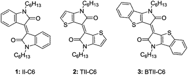 |
| | Fig. 1 Chemical structures of 1–3. | |
Result and discussion
Synthesis and characterization
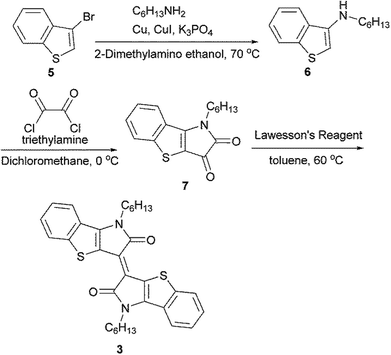
The synthetic routes of 1, 2, and, 3 are shown in Scheme S1.† 1, 4 and 5 were prepared according to previous reports.27,36,37 For the synthesis of 3, the Ullmann-type amination of 3-bromobenzothiophene 5 with hexylamine afforded the aminated product 6. The subsequent treatment with oxalyl chloride provided the corresponding isatin 7. The coupling reaction of isatin 7 using Lawesson's reagent gave compound 3 (Scheme 1). The detailed synthesis procedures are described in the ESI.† The decomposition temperature defined as the 5% weight loss estimated from a thermal gravimetric analysis (TGA) were 299 °C for 1, 296 °C for 2 and 367 °C for 3 (Fig. S1†). Except for molecule 3, the melting points were observed at 113 °C for 1 and 122 °C for 2. These observations indicated that the extended π-conjugation of the planar backbone improved the thermal stability, which is probably related to forming the tight intermolecular π–π stacking due to the enhanced π–π intermolecular interactions.
 |
| | Scheme 1 Synthetic route of 3. | |
Theoretical calculations
To evaluate the electronic structures and optimized geometries of 1–3, density functional theory (DFT) calculations using the Gaussian 09 program based on the B3LYP/6-31G+(d,p) level have been performed on methyl-substituted molecules.38 Fig. 2 shows the energy-minimized structures and the corresponding HOMO and LUMO orbitals of the methyl-substituted 1–3. The optimized molecular geometries of 2 and 3 are completely flat structures, while 1 is twisted by 12.9° at the central double bond. These results imply that TII and BTII are desirable materials for carrier-transport since a high planar backbone often reinforces the π–π interactions to form a high crystalline film.30 The HOMO and LUMO orbitals of all molecules are well delocalized over the π-conjugated skeletons. The calculated HOMO and LUMO levels are −5.89 eV and −2.99 eV for 1, −5.32 eV and −2.84 eV for 2, and −5.19 eV and −3.08 eV for 3, respectively. The high-lying HOMO and low-lying LUMO reduce the bandgap in the order of 1 < 2 < 3.
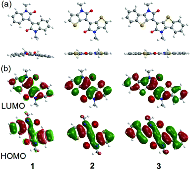 |
| | Fig. 2 (a) Optimized molecular geometries and (b) the calculated distributions of the HOMO and LUMO orbitals of methyl-substituted 1–3 estimated from the DFT calculations. | |
Optical and electrochemical properties
The optical and electrochemical properties of 1–3 have been investigated by UV-vis absorption spectroscopy and cyclic voltammetry (CV), and the data are listed in Table 1. Fig. 3 shows the UV-vis absorption spectra of 1–3 in a 10−5 M chloroform solution and spin-coated thin films. All molecules exhibited the dual main absorption bands in both a solution and thin film, which consist of relatively strong bands in the high-energy region (350–400 nm for 1 and 2 and 370–470 nm for 3) and broad bands in the low-energy region (400–550 nm for 1, 450–550 nm for 2, and 500–800 nm for 3). The low energy absorption bands in solution were remarkably red-shifted in the order of 1 < 2 < 3 along with the enhanced molar extinction coefficient (εmax), indicating that this observation is basically consistent with the order of the molecular planarity and π-conjugation length. Compared to the solution spectra, the absorption spectra in the thin films of 2 and 3 showed an obvious red-shift, suggesting a considerable intermolecular aggregation in the solid state. Especially, the appearance of the more structural peaks for 2 and 3 than that for 1 would be due to the flat molecular structures enhancing the intermolecular π–π interactions. The optical bandgaps (Eoptg) estimated from the absorption onset in solution are 2.03 eV for 1, 1.88 eV for 2, and 1.57 eV for 3, agreeing with the DFT calculation results.
Table 1 Optical and electrochemical properties of 1–3
| |
λsol.maxa (εmaxa) [nm] ([104 M−1 cm−1]) |
λfilmmaxb [nm] |
Eopt.gc [eV] |
ECVHOMOd [eV] |
ECVLUMOd [eV] |
ECVge [eV] |
| In CHCl3 solution. Spin-coat thin films. Estimated from the solution absorption onset. Estimated from cyclic voltammetry vs. Fc/Fc+ (EHOMO = −4.80 eV). ECVg = ECVLUMO − ECVHOMO. |
| 1 |
395 (1.29), 500 (0.41) |
378, 501 |
2.03 |
−5.41 |
−3.10 |
2.31 |
| 2 |
381 (1.25), 401 (1.10), 552 (0.91) |
388, 409, 567 |
1.88 |
−5.21 |
−3.35 |
1.86 |
| 3 |
419 (1.83), 437 (1.81), 651 (1.30) |
437, 678, 733 |
1.57 |
−5.07 |
−3.38 |
1.69 |
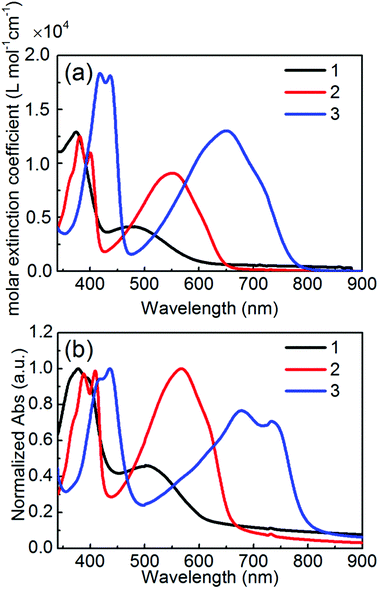 |
| | Fig. 3 UV-vis absorption spectra of 1–3 for (a) 10−5 M CHCl3 solutions and (b) thin films spin-coated from CHCl3 solutions. | |
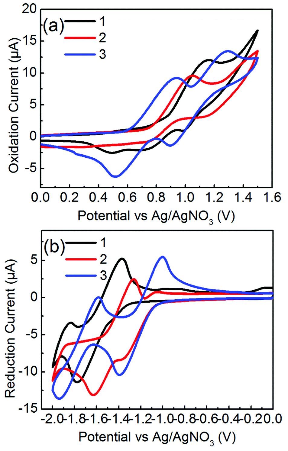
The electrochemical potentials of EHOMO and ELUMO were determined from the onset oxidation potentials and reduction potentials of the cyclic voltammograms, which were calibrated by ferrocene/ferrocenium (Fc/Fc+), whose redox potential was assumed to be −4.8 eV under vacuum level (Fig. 4).39 Molecules 1 and 2 exhibited irreversible oxidation and reduction profiles whereas 3 clearly exhibited two separated reversible oxidation and reduction couples. Molecule 2 has higher HOMO and lower LUMO levels by ca. 0.2 eV than those of 1. This observation is related to the release of the steric twist of 1 to form the flat π-framework of 2. Of particular note is that 3 has a high-lying HOMO level and almost the same LUMO level as 2, suggesting that the π-extension of 3, in which additional phenyl rings are fused to the TII unit, contributes to the increase in the HOMO level without changing the LUMO level. The resulting HOMO–LUMO gaps (ECVg) are 2.31 eV for 1, 1.86 eV for 2, and 1.69 eV for 3, which are consistent with the optical bandgap trend. In general, the ambipolar characteristics for Au electrodes require a HOMO level above −5.6 eV and LUMO level below −3.15 eV.40 The HOMO and LUMO levels of 2 and 3 satisfy these conditions. Therefore, molecules 2 and 3 are expected to exhibit an ambipolar performance in OFETs.
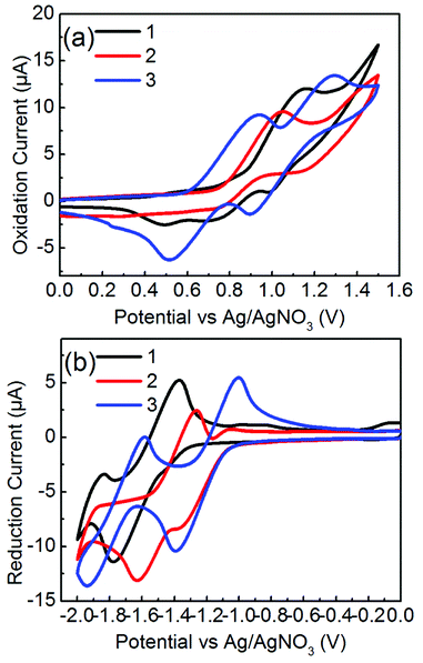 |
| | Fig. 4 Cyclic voltammograms of 1–3 measured in 0.1 M Bu4NPF6 in CH2Cl2 at the scan rate of 100 mV s−1, (a) positive scans for oxidation steps and (b) negative scans for reducing steps. | |
X-ray single-crystal structure analysis
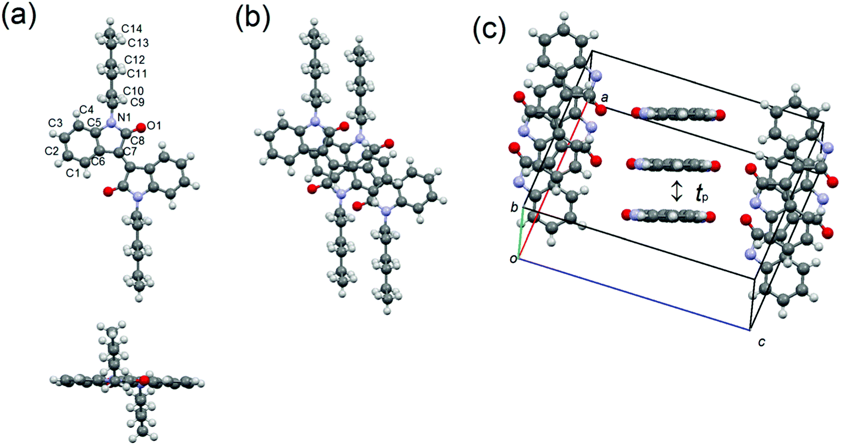
The X-ray structure analyses of 1–3 have been performed using single crystals grown by the slow diffusion of methanol into the chloroform solutions of 1 and 2 and chloroform into toluene solutions of 3. The crystallographic data are listed in Table 2, and the molecular and crystal structures are shown in Fig. 5–7. Molecule 1 crystallizes in the monoclinic system with space group P21/c. A half molecule, which is associated with the 2-fold axis along the c axis, is crystallographically independent (Fig. 5). Unlike the optimized structure estimated from the DFT calculation, the π-framework is almost planar in the solid state, and the alkyl chains are extended out of the planes. The molecules stack into one-dimensional slipped columnar structures along the b axis with the interplanar spacing of 3.33 Å, in which the slip distances of 1 are 2.90 Å along the molecular long axis and 2.30 Å along the molecular short axis (Fig. 5(b)). Assuming the tight binding method,41 the calculated the HOMO and LUMO transfer integrals, tp = 68 meV for HOMO and tp = 51 meV for LUMO, also indicate a one-dimensional transport (Fig. 5(c)).
Table 2 Crystallographic data for 1–3
| |
1 |
2 |
3 |
| R1 = ∑||F0| − |Fc||/∑|F0|. RW = [∑ω(|F0| − |Fc|)2/∑ωF02]1/2. |
| Chemical formula |
C28H34N2O2 |
C24H30N2O2S2 |
C32H34N2O2S2 |
| Crystal system |
Monoclinic |
Monoclinic |
Triclinic |
| Formula weight |
430.59 |
442.63 |
542.75 |
| Sharp |
Red needle |
Black plate |
Black needle |
| Space group |
P21/c |
P21/c |
P(![[1 with combining macron]](https://www.rsc.org/images/entities/char_0031_0304.gif) ) ) |
| a(Å) |
14.8546(3) |
19.2970(3) |
5.05526(9) |
| b(Å) |
4.93706(9) |
8.24241(10) |
8.31652(15) |
| c(Å) |
16.1007(4) |
15.6572(2) |
16.4731(3) |
| α(o) |
90.0000 |
90.0000 |
79.8632(10) |
| β(o) |
92.2269(13) |
114.8240 |
87.7600(12) |
| γ(o) |
90.0000 |
90.0000 |
86.0505(10) |
| V(Å3) |
1179.91(4) |
2260.24(6) |
679.88(3) |
| Z |
2 |
4 |
1 |
| Dcal(g cm−3) |
1.212 |
1.301 |
1.326 |
| Data/parameters |
2150/145 |
4124/271 |
2436/172 |
| Goodness of fit on F02 |
1.100 |
1.075 |
1.137 |
| R1a/RWb |
0.0359/0.1018 |
0.0399/0.1094 |
0.0475/0.1455 |
| Reflections used |
2150 |
4124 |
2436 |
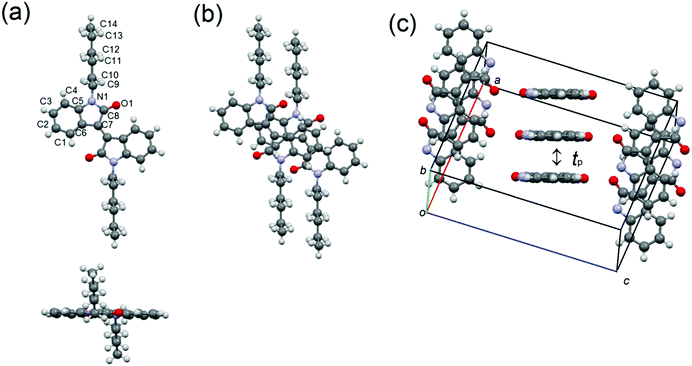 |
| | Fig. 5 (a) Molecular structure, (b) overlap mode, and (c) molecular packing of 1, in which alkyl chains are omitted for clarification. | |
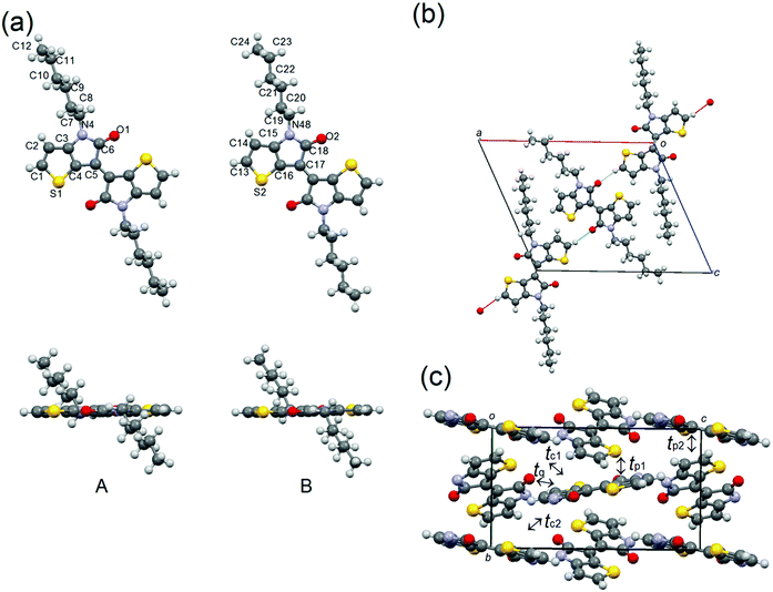 |
| | Fig. 6 (a) Molecular structure, (b) H-bonding chains along the a + c direction, and (c) molecular packing of 2, in which the alkyl chains are omitted for clarification. | |
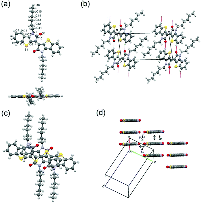 |
| | Fig. 7 (a) Molecular structure, (b) H-bonding chains along the b axis, (c) overlap mode, and (d) molecular packing of 3, in which alkyl chains are omitted for clarification. | |
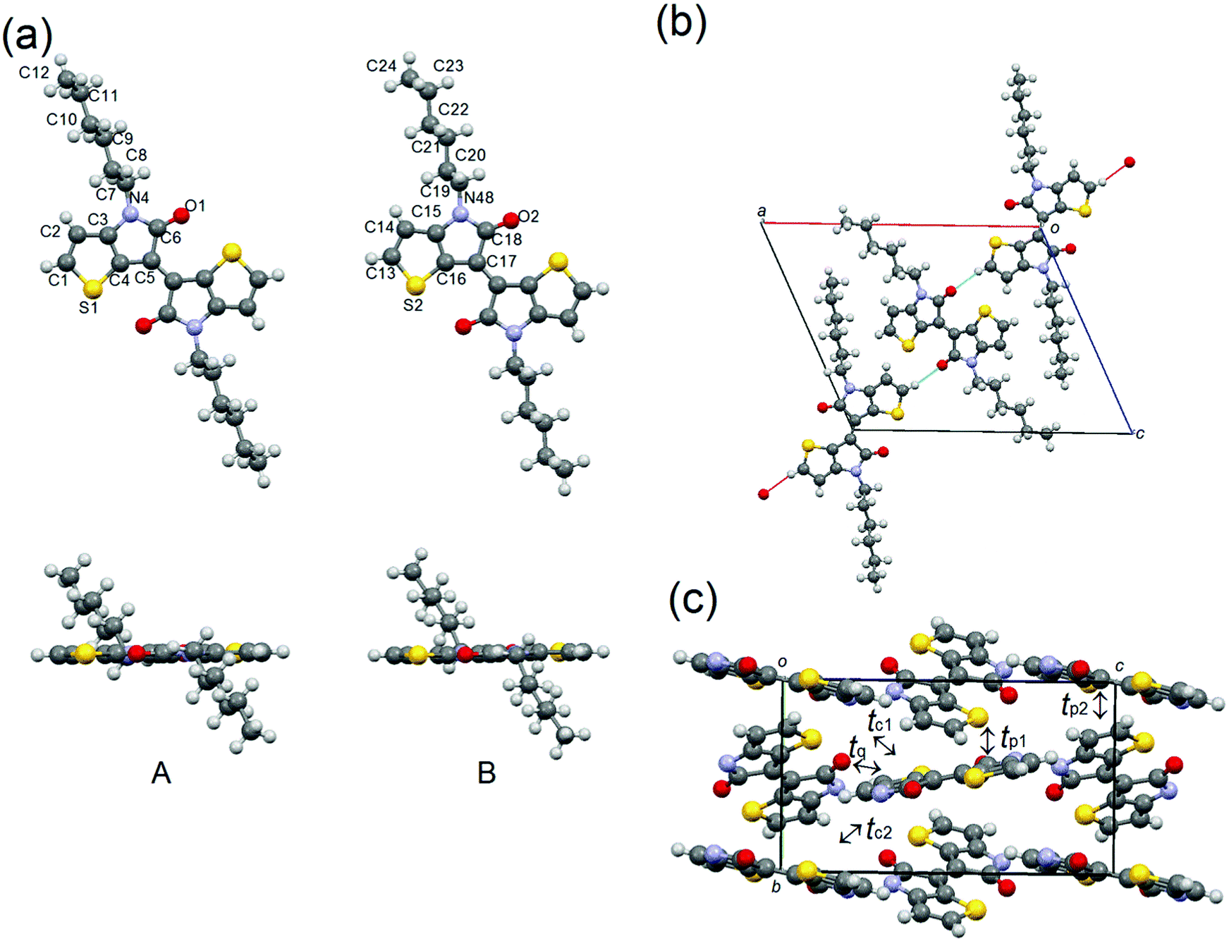
Molecule 2 crystallizes with the same P21/c space group as molecule 1, in which the two half molecules A and B are crystallographically independent (Fig. 6). As expected, the TII unit of the A and B molecules adopt planar conformations, and the alkyl chains are extended out of plane. In the crystal structure, molecules A and B are connected through the H-bonding between the α-protons of thiophene and carbonyl oxygens to form infinite chains aligning along the a + c direction (Fig. 5(b)). No noticeable intermolecular overlaps, desirable for charge-transport, are observed in the structure. Therefore, the calculated HOMO and LUMO transfer integrals are quite low: tp1 = 6 meV, tp2 = 3 meV, tq = 3 meV, tc1 = 2 meV and tc2 = 2 meV for HOMO integrals and tp1 = 2 meV, tp2 = 1 meV, and tq = 12 meV for LUMO integrals (Fig. 6(c)). These small values imply the low charge-carrier mobilities of 2.
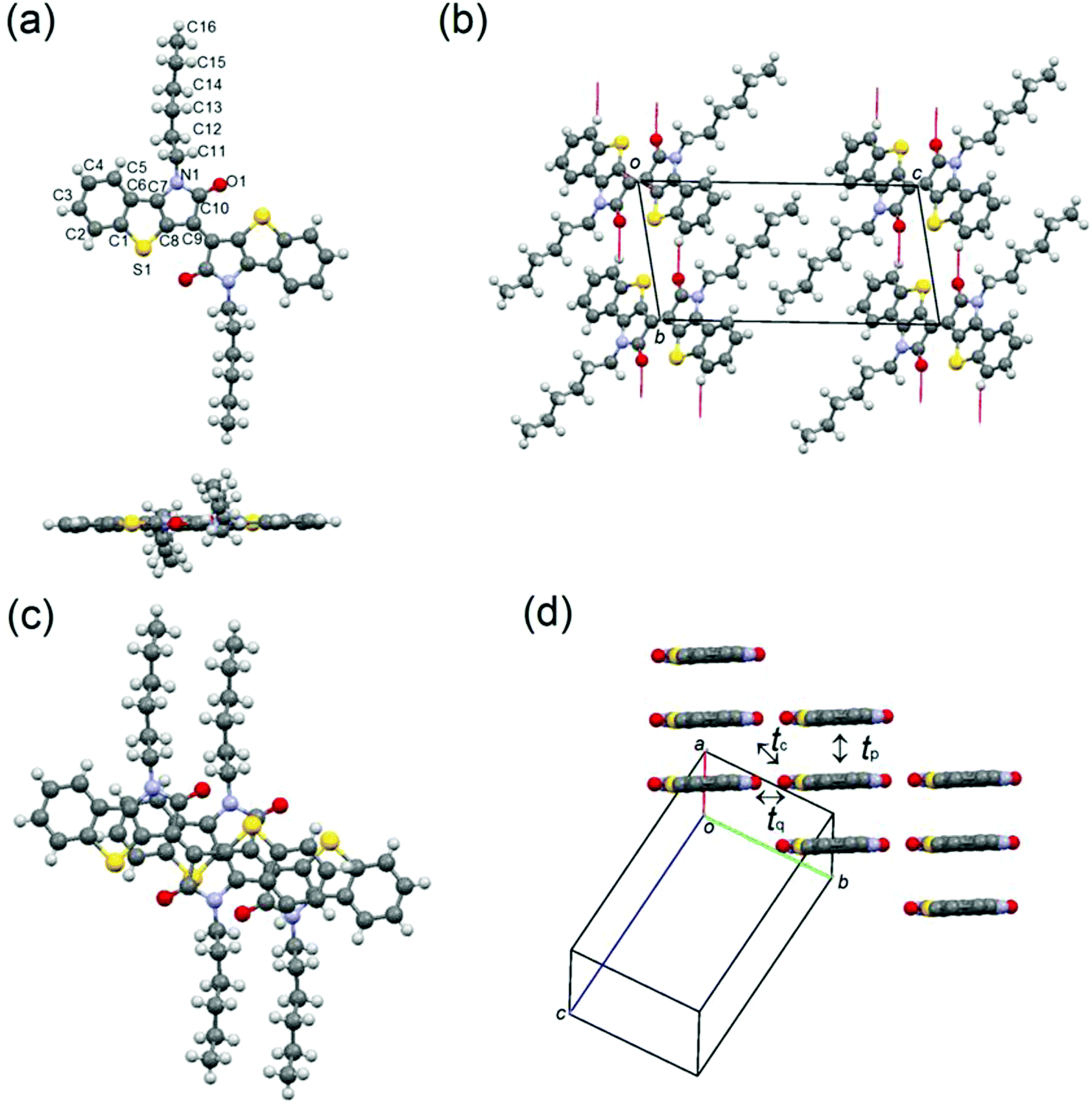
Molecule 3 crystallizes in a triclinic system with the space group P(), in which the half molecules are crystallographically independent (Fig. 7). The π-framework of 3 has a flat conformation, and the alkyl chains are extended in-plane. Similar to the structure of 1, the molecules make one-dimensional slipped stacks along the a axis with the interplanar spacing of 3.40 Å, and the slip distances of 3 are 3.47 Å along the molecular long axis and 1.52 Å along the molecular short axis. The π-stacks connected through the infinite H-bonding chains along the b axis are aligned with a parallel orientation, which is indicative of the presence of side-by-side interactions in contrast to the structure of 1. The calculated HOMO transfer integrals along the stacks are tp = 69 meV, tq = 2 meV, and tc = 2 meV and the LUMO transfer integrals are tp = 57 meV, tq = 3 meV, and tc = 3 meV (Fig. 7(c)). These anisotropic intermolecular interactions also suggest that molecule 3 makes a one-dimensional transport.
Field-effect transistor performance
In order to investigate the charge transport properties of 1–3, we fabricated bottom-gate/top-contact OFET devices with Au as the source and drain electrodes. The thin films (45 nm) were thermally deposited on the tetratetracontane (TTC)-modified SiO2/Si substrates. All the molecules 1–3 exhibited typical ambipolar FET performances, and the corresponding data are summarized in Table 3. The transfer and output curves are provided in Fig. 8 and S2,† respectively. These results are because the energy levels of molecules 1–3 (Table 1) satisfy the requirements to display ambipolar characteristics (−5.6 to −3.15 eV).40 Molecules 1 and 2 exhibited low hole and electron mobilities around 10−5–10−4 cm2 V−1 s−1. In contrast, molecule 3 exhibited the highest hole mobility of 0.095 cm2 V−1 s−1 and electron mobility of 5.8 × 10⁻³ cm2 V−1 s−1. These values are comparable or slightly improved compared to the TII-based copolymers24,31 and the previously reported TII-based small molecules.28 This p-channel dominant character is because the HOMO level estimated from the CV measurement matches the Fermi level (−5.13 eV) of the Au electrode,42 therefore, facilitating the effective hole injection from the Au electrodes to the thin film.
Table 3 OFET characterization for 1–3
| |
p-type |
n-type |
| μavg (μmax) [cm2 V−1 s−1] |
Vth [V] |
Ion/Ioff |
μavg (μmax) [cm2 V−1 s−1] |
Vth [V] |
Ion/Ioff |
| 1 |
3.7 × 10⁻⁴ (7.1 × 10⁻⁴) |
−64.5 |
105 |
2.2 × 10⁻⁵ (4.1 × 10⁻⁵) |
48.4 |
103 |
| 2 |
1.2 × 10⁻⁵ (1.6 × 10⁻⁵) |
−115.8 |
103 |
1.0 × 10⁻⁴ (1.3 × 10⁻⁴) |
77.7 |
104 |
| 3 (TTC) |
0.089 (0.095) |
5.0 |
105 |
4.3 × 10⁻³ (5.8 × 10⁻³) |
76.7 |
104 |
| 3 (OTMS r.t) |
0.088 (0.14) |
−11.3 |
104 |
N/A |
|
|
| 3 (OTMS 80 °C) |
0.13 (0.18) |
−2.4 |
104 |
N/A |
|
|
| 3 (OTMS 100 °C) |
0.094 (0.12) |
2.95 |
104 |
N/A |
|
|
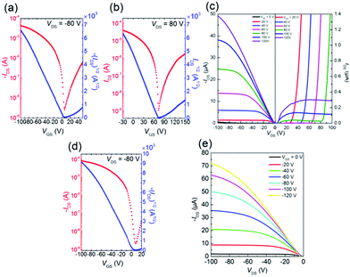 |
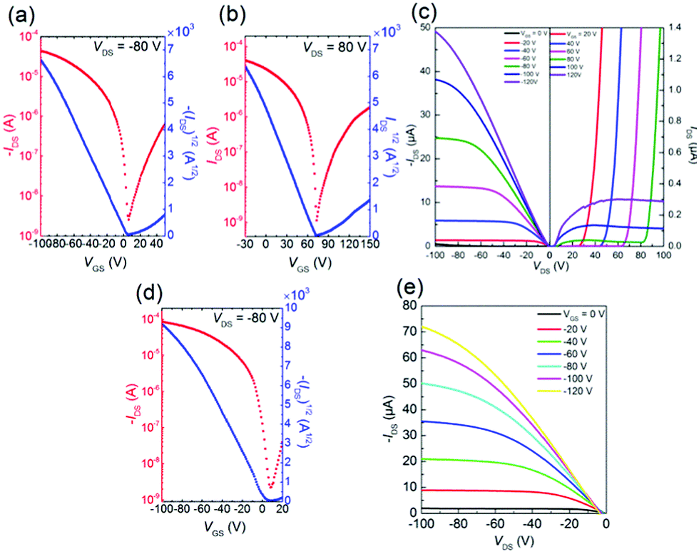
| | Fig. 8 (a) p-type and (b) n-type transfer curves, and (c) output curve for the TTC modified device of 3. (d) p-type transfer curve and (e) output curve for the OTMS modified substrate elevated at 80 °C of 3. | |
The structure analyses of 1 and 3 indicate a similar one-dimensional transport system. However, the higher mobilities are achieved in the thin film of 3. This result suggests that the increased π-conjugation of the BTII unit enables significant co-facial π–π interactions, realizing a tight intermolecular packing.
In general, the substrate temperature during thermal evaporation influences microstructure and morphology in thin film, and thus we deposited thin film of 3 at an elevated temperature (80 °C and 100 °C) on the octadecyltrimethoxysilane (OTMS)-modified SiO2/Si substrates. The transfer and output curves are listed in Fig. 8 and S2.† The thin film of 3 deposited on the OTMS-modified substrate at 80 °C exhibited p-type performance with higher hole mobility of μh,max = 0.18 cm2 V−1 s−1 than that of the device on the TTC-modified substrate. The SAM modification has strong impact of carrier transport polarity: the observed ambipolar behavior on the TTC-modified substrate beneficial for electron-transport basically accords with the previous report.43
Morphology of thin films
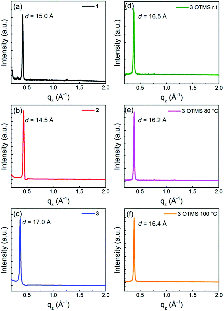
In order to clarify the difference in the FET properties, the thin film microstructure and surface topology of 1–3 on the TTC-modified substrates and 3 on the OTMS-modified substrates, XRD patterns (Fig. 9) and AFM images (Fig. 10) were examined. All the XRD patterns show the primary sharp and intense peaks corresponding to the d-spacings of 15.0 Å for 1, 14.5 Å for 2, 17.0 Å for 3 on the TTC-modified substrates and 16.5 Å at r.t, 16.2 Å at 80 °C, and 16.4 Å at 100 °C for 3 on the OTMS-modified substrates. Considering the bulk crystal lattice estimated from the single-crystal X-ray structure analyses, these d-spacings approximately correspond to a for 1, c![[thin space (1/6-em)]](https://www.rsc.org/images/entities/char_2009.gif) sinβ for 2, and b + c for 3 on the TTC-modified substrates and c at r.t, csinα at 80 °C, and csinβ at 100 °C for 3 on the OTMS-modified substrates. Thus, in the layered out-of-plane direction, the molecular π-frameworks of 1–3 are tilted, and both sets of hexyl chains stand on the substrate; tilt angles are roughly estimated to be 47° for 1, 9° for 2, 20° for 3 on the TTC-modified substrates and 35° at r.t, 30° at 80 °C, and 34° at 100 °C for 3 on the OTMS-modified substrates. In general, the small tilt angle is one of the factors for maximizing the carrier mobility since the charge-transport channel is parallel to the substrate.44 Therefore, the large tilt angle of 1 is unfavorable for charge carrier transport, thus leading to the low mobility. In contrast, thin film of 2 showed low mobility in spite of the smallest tilt angle among 1–3, which would be attributed to poor transfer integrals calculated from the single-crystal X-ray structure analyses. The higher mobility of 3 in comparison with 1 and 2 are owing to the tilt angles around 20–34° with large transfer integrals coming from dense molecular packing and molecular size.
sinβ for 2, and b + c for 3 on the TTC-modified substrates and c at r.t, csinα at 80 °C, and csinβ at 100 °C for 3 on the OTMS-modified substrates. Thus, in the layered out-of-plane direction, the molecular π-frameworks of 1–3 are tilted, and both sets of hexyl chains stand on the substrate; tilt angles are roughly estimated to be 47° for 1, 9° for 2, 20° for 3 on the TTC-modified substrates and 35° at r.t, 30° at 80 °C, and 34° at 100 °C for 3 on the OTMS-modified substrates. In general, the small tilt angle is one of the factors for maximizing the carrier mobility since the charge-transport channel is parallel to the substrate.44 Therefore, the large tilt angle of 1 is unfavorable for charge carrier transport, thus leading to the low mobility. In contrast, thin film of 2 showed low mobility in spite of the smallest tilt angle among 1–3, which would be attributed to poor transfer integrals calculated from the single-crystal X-ray structure analyses. The higher mobility of 3 in comparison with 1 and 2 are owing to the tilt angles around 20–34° with large transfer integrals coming from dense molecular packing and molecular size.
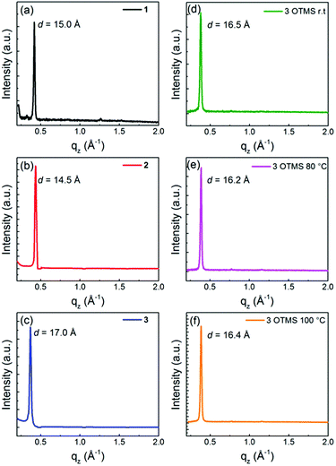 |
| | Fig. 9 X-ray diffraction patterns of (a) 1, (b) 2 and (c) 3 thin films (45 nm) deposited on TTC (20 nm) modified substrates and thin film of 3 deposited elevated substrate temperature at (d) r.t, (e) 80 °C, and (f) 100 °C. | |
 |
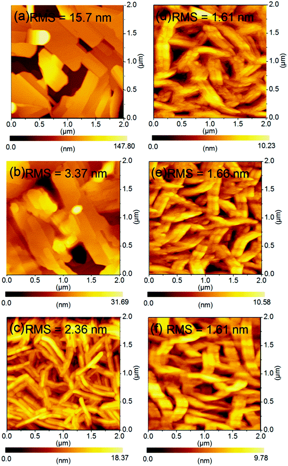
| | Fig. 10 AFM images of thin films (45 nm) of (a) 1, (b) 2 and (c) 3 thermally evaporated on TTC (20 nm) modified substrates and thin film of 3 deposited elevated substrate temperature at (d) r.t, (e) 80 °C, and (f) 100 °C. | |
We next compared the AFM height images of 1–3 in order to understand the FET performances of 1–3. The different FET properties should also originate from the surface morphologies of the thin films, because microscopic thin film structures have a large impact on the charge-transport.45 The thin film of 1 showed the largest plate-like grains among molecules 1–3, however, these grains are separated by obviously disconnected and defective boundaries bearing void-like structures, indicative of a high RMS value. This poor surface morphology is the origin of the low mobilities of 1 as well as the large tilt angle normal to the substrate. Similarly, the thin film of 2 exhibited discontinuous plate-like domains, although the surface roughness was even reduced. This defective thin film morphology is responsible for the low carrier mobilities as well as the smaller intermolecular overlaps. The most important change was observed in the thin film of 3. Molecule 3 formed well-interconnected nanorod-like crystalline grains with the lowest RMS value. The fabrication conditions for the thin films of 1–3 are the same. Therefore, the extended π-conjugation of 3 would contribute to forming the crystalline grains which are laterally grown via an island-like mechanism.46 As a result, the obtained surface morphology of 3 consists of nanorod-like crystalline grains, which makes dense and smoothly connected domains preferable for charge transport. All thin films of 3 deposited on the OTMS-modified substrate are consisted of larger nanorod-like crystalline grains compared with that of 3 on the TTC-modified substrate, especially when comparing the deposited films at r.t. (Fig. 10(c)–(f)), suggesting SAM treatment has a significant effect on film formation. Among thin films on the OTMS-modified substrate, the dense domains and interconnected grain boundaries are formed in addition to the smallest tilt angle in thin film deposited at 80 °C. This is responsible for the highest mobilities of 0.18 cm2 V−1 s−1 of 3. These findings concerning the thin-film microstructures of 1–3 would suggest that the molecular π-surface has a strong impact on the film-formation mechanism.
Conclusions
In this study, we have synthesized and characterized three sets of molecules 1–3 with hexyl side chains in order to understand the structure–property relationship in the FETs. In particular, the BTII of 3 is a novel π-expanded framework of TII. The absorption spectra are remarkably red-shifted in the order of 1 < 2 < 3 along with the enhanced molar extinction coefficient in the low-energy region. The high-lying HOMO and low-lying LUMO levels are realized by the molecular planarity and extended π-conjugation, and then the smaller bandgap of 3 is realized. The single crystal structures of 1–3 were analyzed. Molecules 1 and 3 are packed into one-dimensional columns composed of co-facial intermolecular overlaps whereas molecule 2 does not form noticeable intermolecular overlaps. The OFET of 1–3 on the TTC-modified substrates exhibited ambipolar characteristics. Notably, the thin film of 3 on the TTC modified device showed a p-dominant performance with the highest hole mobility of 0.095 cm2 V−1 s−1 and electron mobility of 5.8 × 10⁻³ cm2 V−1 s−1, which is well associated with the HOMO energy level of 3. On the OTMS-modified substrate, the devices of 3 showed a p-type performance with the mobility up to 0.18 cm2 V−1 s−1. Systematic evaluation of the FET performance on the TTC-modified substrate by comparing three sets of molecules 1–3 concluded that the π-expansion of the TII unit, namely the BTII unit, influences the electronic structure, packing motif in the bulk crystal, and thin film structure, resulting in the improved FET performance. The present study provides a better understanding of the structure–property relationship of the TII-based molecules for the development of high performance ambipolar OFETs.
Acknowledgements
This study was partly supported by a fund from the Development of Human Resources in Science and Technology of the Japan Science and Technology Agency, JST (for H. M.) and a Grant-in-Aid for Scientific Research (C) (No. 26410087) from the Ministry of Education, Culture, Sports, Science and Technology (for M. A). The authors are grateful to the Center for Advanced Materials, Tokyo Institute of Technology, for the microanalysis.
Notes and references
- C. L. Wang, H. L. Dong, W. P. Hu, Y. Q. Liu and D. B. Zhu, Chem. Rev., 2012, 112, 2208–2267 CrossRef CAS PubMed.
- A. R. Murphy and J. M. J. Fréchet, Chem. Rev., 2007, 107, 1066–1096 CrossRef CAS PubMed.
- H. Klauk, Chem. Soc. Rev., 2010, 39, 2643–2666 RSC.
- J. E. Anthony, A. Facchetti, M. Heeney, S. R. Marder and X. Zhan, Adv. Mater., 2010, 22, 3876–3892 CrossRef CAS PubMed.
- J. Zaumseil and H. Sirringhaus, Chem. Rev., 2007, 107, 1296–1323 CrossRef CAS PubMed.
- H. Yan, Z. Chen, Y. Zheng, C. Newman, J. R. Quinn, F. Dötz, M. Kastler and A. Facchetti, Nature, 2009, 457, 679–686 CrossRef CAS PubMed.
- J. Li, Y. Zhao, H. S. Tan, Y. Guo, C.-A. Di, G. Yu, Y. Liu, M. Lin, S. H. Lim, Y. Zhou, H. Su and B. S. Ong, Sci. Rep., 2012, 2, 754–763 Search PubMed.
- G. Kim, S.-J. Kang, G. K. Dutta, Y.-K. Han, T. J. Shin, Y.-Y. Noh and C. Yang, J. Am. Chem. Soc., 2014, 136(26), 9477–9483 CrossRef CAS PubMed.
- C. Luo, A. K. K. Kyaw, L. A. Perez, S. Patel, M. Wang, B. Grimm, G. C. Bazan, E. J. Kramer and A. J. Heeger, Nano Lett., 2014, 14(5), 2764–2771 CrossRef CAS PubMed.
- S. Fabiano, H. Usta, R. Forchheimer, X. Crispin, A. Facchetti and M. Berggren, Adv. Mater., 2014, 26(44), 7438–7443 CrossRef CAS PubMed.
- K.-J. Baeg, J. Kim, D. Khim, M. Caironi, D.-Y. Kim, I.-K. You, J. R. Quinn, A. Facchetti and Y.-Y. Noh, ACS Appl. Mater. Interfaces, 2011, 3(8), 3205–3214 CAS.
- M. A. McCarthy, B. Liu, E. P. Donoghue, I. Kravchenko, D. Y. Kim, F. So and A. G. Rinzler, Science, 2011, 332, 570–573 CrossRef CAS PubMed.
- M. C. Gwinner, D. Kabra, M. Roberts, T. J. Brenner, B. H. Wallikewitz, C. R. McNeill, R. H. Friend and H. Sirringhaus, Adv. Mater., 2012, 24(20), 2728–2734 CrossRef CAS PubMed.
- J. Lee, A.-R. Han, J. Kim, Y. Kim, J. H. Oh and C. Yang, J. Am. Chem. Soc., 2012, 134(51), 20713–20721 CrossRef CAS PubMed.
- J. Lee, A.-R. Han, H. Yu, T. J. Shin, C. Yang and J. H. Oh, J. Am. Chem. Soc., 2013, 135(25), 9540–9547 CrossRef CAS PubMed.
- X. Liu, Y. Sun, B. B. Y. Hsu, A. Lorbach, L. Qi, A. J. Heeger and G. C. Bazan, J. Am. Chem. Soc., 2014, 136(15), 5697–5708 CrossRef CAS PubMed.
- G. C. Welch, L. A. Perez, C. V. Hoven, Y. Zhang, X.-D. Dang, A. Sharenko, M. F. Toney, E. J. Kramer, T.-Q. Nguyen and G. C. Bazan, J. Mater. Chem., 2011, 21, 12700–12709 RSC.
- S. Xu, N. Ai, J. Zheng, N. Zhao, Z. Lan, L. Wen, X. Wang, J. Pei and X. Wan, RSC Adv., 2015, 5, 8340–8344 RSC.
- J. Zhang, G. Wu, C. He, D. Deng and Y. Li, J. Mater. Chem., 2011, 21, 3768–3774 RSC.
- T. Higashino, S. Kumeta, S. Tamura, Y. Ando, K. Ohmori, K. Suzuki and T. Mori, J. Mater. Chem. C, 2015, 3, 1588–1594 RSC.
- O. Pitayatanakul, T. Higashino, T. Kadoya, M. Tanaka, H. Kojima, M. Ashizawa, T. Kawamoto, H. Matsumoto, K. Ishikawa and T. Mori, J. Mater. Chem. C, 2014, 2, 9311–9317 RSC.
- E. Wang, W. Mammo and M. R. Andersson, Adv. Mater., 2014, 26, 1801–1826 CrossRef CAS PubMed.
- R. S. Ashraf, A. J. Kronemeijer, D. I. James, H. Sirringhaus and I. McCulloch, Chem. Commun., 2012, 48, 3939–3941 RSC.
- Y. Koizumi, M. Ide, A. Saeki, C. Vijayakumar, B. Balan, M. Kawamoto and S. Seki, Polym. Chem., 2013, 4, 484–494 RSC.
- G. K. Dutta, A.-R. Han, J. Lee, Y. Kim, J. H. Oh and C. Yang, Adv. Funct. Mater., 2013, 23, 5317–5325 CrossRef CAS PubMed.
- C.-M. Chen, S. Sharma, Y.-L. Li, J.-J. Lee and S.-A. Chen, J. Mater. Chem. C, 2015, 3, 33–36 RSC.
- R. R. Dasari, A. Dindar, C. K. Lo, C.-Y. Wang, C. Quinton, S. Singh, S. Barlow, C. F. Hernandez, J. R. Reynolds, B. Kippelen and S. R. Marder, Phys. Chem. Chem. Phys., 2014, 16, 19345–19350 RSC.
- T. Odajima, M. Ashizawa, Y. Konosu, H. Matsumoto and T. Mori, J. Mater. Chem. C, 2014, 2, 10455–10467 RSC.
- G. W. P. V. Pruissen, F. Gholamrezaie, M. M. Wienk and R. A. J. Janssen, J. Mater. Chem., 2012, 22, 20387–20393 RSC.
- M. S. Chen, J. R. Niskala, D. A. Unruh, C. K. Chu, O. P. Lee and J. M. Fréchet, Chem. Mater., 2013, 25, 4088–4096 CrossRef CAS.
- M. Ide, Y. Koizumi, A. Saeki, Y. Izumiya, H. Ohkita, S. Ito and S. Seki, J. Phys. Chem. C, 2013, 117, 26859–26870 CAS.
- M. Karakawa and Y. Aso, Macromol. Chem. Phys., 2013, 214, 2388–2397 CrossRef CAS PubMed.
- M. Karakawa and Y. Aso, RSC Adv., 2013, 3, 16259–16263 RSC.
- M. Ide, Y. Koizumi, A. Saeki and S. Seki, J. Photopolym. Sci. Technol., 2013, 26(2), 217–221 CrossRef CAS.
- H.-J. Yun, H. H. Choi, S.-K. Kwon, Y.-H. Kim and K. Cho, ACS Appl. Mater. Interfaces, 2015, 7, 5898–5906 CAS.
- L. A. Estrada, D. Y. Liu, D. H. Salazar, A. L. Dyer and J. R. Reynolds, Macromolecules, 2012, 45, 8211–8220 CrossRef CAS.
- J. Youn, M.-C. Chen, Y.-J. Liang, H. Huang, R. P. Ortiz, C. Kim, C. Stern, T.-S. Hu, L.-H. Chen, J.-Y. Yan, A. Facchetti and T. J. Marks, Chem. Mater., 2010, 22, 5031–5041 CrossRef CAS.
- M. J. Frisch, G. W. Trucks, H. B. Schlegel, G. E. Scuseria, M. A. Robb, J. R. Cheeseman, G. Scalmani, V. Barone, B. Mennucci, G. A. Petersson, H. Nakatsuji, M. Caricato, X. Li, H. P. Hratchian, A. F. Izmaylov, J. Bloino, G. Zheng, J. L. Sonnenberg, M. Hada, M. Ehara, K. Toyota, R. Fukuda, J. Hasegawa, M. Ishida, T. Nakajima, Y. Honda, O. Kitao, H. Nakai, T. Vreven, J. A. Montgomery Jr, J. E. Peralta, F. Ogliaro, M. Bearpark, J. J. Heyd, E. Brothers, K. N. Kudin, V. N. Staroverov, R. Kobayashi, J. Normand, K. Raghavachari, A. Rendell, J. C. Burant, S. S. Iyengar, J. Tomasi, M. Cossi, N. Rega, N. J. Millam, M. Klene, J. E. Knox, J. B. Cross, V. Bakken, C. Adamo, J. Jaramillo, R. Gomperts, R. E. Stratmann, O. Yazyev, A. J. Austin, R. Cammi, C. Pomelli, J. W. Ochterski, R. L. Martin, K. Morokuma, V. G. Zakrzewski, G. A. Voth, P. Salvador, J. J. Dannenberg, S. Dapprich, A. D. Daniels, Ö. Farkas, J. B. Foresman, J. V. Ortiz, J. Cioslowski and D. J. Fox, The molecular orbital calculation was carried out using the Gaussian 09, Revision B.01, Gaussian, Inc., Wallingford CT, 2009 Search PubMed.
- J. Pommerehne, H. Vestweber, W. Guss, R. F. Mark, H. Bässeles, M. Porsch and J. Daub, Adv. Mater., 1995, 7, 551–554 CrossRef CAS PubMed.
- M. L. Tang, A. D. Reichardt, P. Wei and Z. Bao, J. Am. Chem. Soc., 2009, 131, 5264 CrossRef CAS PubMed.
- T. Mori, A. Kobayashi, Y. Sasaki, H. Kobayashi, G. Saito and H. Inokuchi, Bull. Chem. Soc. Jpn., 1984, 57, 627–633 CrossRef CAS.
- H. B. Michaelson, J. Appl. Phys., 1977, 48, 4729–4733 CrossRef CAS PubMed.
- M. Irimia-Vladu, E. D. Głowacki, P. A. Troshin, G. Schwabegger, L. Leonat, D. K. Susarova, O. Krystal, M. Ullah, Y. Kanbur, M. A. Bodea, V. F. Razumov, H. Sitter, S. Bauer and N. S. Sariciftci, Adv. Mater., 2012, 24, 375–380 CrossRef CAS PubMed.
- T. Kakinuma, H. Kojima, M. Ashizawa, H. Matsumoto and T. Mori, J. Mater. Chem. C, 2013, 1, 5395–5401 RSC.
- H. N. Tsao and K. Müllen, Chem. Soc. Rev., 2010, 39, 2372–2386 RSC.
- J. A. Venebles, G. D. T. Spiller and M. Hanbücken, Rep. Prog. Phys., 1984, 47, 399–459 CrossRef.
Footnote |
| † Electronic supplementary information (ESI) available: Additional information on material synthesis, thermal properties, X-ray single crystal structure analysis, and fabrication and characterization of organic field-effect transistors. CCDC 1061785–1061787. For ESI and crystallographic data in CIF or other electronic format see DOI: 10.1039/c5ra07660a |
|
| This journal is © The Royal Society of Chemistry 2015 |
Click here to see how this site uses Cookies. View our privacy policy here. 
 Open Access Article
 This Open Access Article is licensed under a Creative Commons Attribution-Non Commercial 3.0 Unported Licence