DOI:
10.1039/C5RA06921A
(Paper)
RSC Adv., 2015,
5, 49708-49718
Morphological evolution of gold nanoparticles on silicon nanowires and their plasmonics†
Received
17th April 2015
, Accepted 29th May 2015
First published on 29th May 2015
Abstract
One-dimensional heterostructures composed of silicon (Si) nanowires and uniformly decorated with gold (Au) nanoparticles were fabricated and used as a substrate for organic detection based on the surface-enhanced Raman spectroscopy. Si nanowires were grown via a silane-based chemical vapor deposition approach. The controlled decoration of Au nanoparticles on the Si nanowires was achieved using wet-chemical nucleation and followed by a thermal treatment process. Various annealing parameters were studied to control the shape, size, and surface dispersion of Au nanoparticles on the heterostructures. Microscopic methods were used to evaluate the configuration or morphological evolution (size, inter-particle spacing and density) of nanoparticles at different annealing conditions. The influence of annealing on the chemical composition of Au nanoparticles were analyzed using X-ray photoelectron spectroscopy (XPS) and the phase transformation kinetics was also studied. Finally, surface-enhanced Raman spectroscopy was used to sense organic species and this was studied for various morphologies of nanowire heterostructures.
Introduction
Surface-enhanced Raman spectroscopy (SERS) has been considered as a powerful analytical tool allowing for significantly-enhanced Raman signals for the target molecules with even a single molecule sensitivity.1,2 In this regard, nanostructured gold and silver have been widely studied as SERS substrates due to their excellent surface plasmonic properties (or localized surface plasmon resonance, LSPR).3–6 LSPR can be effectively modulated by controlling the size, shape, and arrangement of the nanostructures,7,8 or by using suitable supporting materials. Direct dispersion or patterning of the nanostructures on a flat substrate, for instance, has been widely reported.9,10 However, further development of such SERS substrates is limited by the poor nanostructure density, uncontrollable aggregation, and nonuniform distribution of the nanostructures.11 Recently, heterostructures of one-dimensional nanowires integrated with extraneous nanoparticles were demonstrated to be of great interest due to their excellent detection sensitivity, reproducibility, stability, and biocompatibility.12,13
Silicon (Si) nanowires have been utilized in bioelectronics, nanoelectronics, optical devices, and energy devices.14–16 The pristine Si nanowires only exhibit moderate Raman sensitivity for molecular detection, and thus proper surface modification or heterostructuring of the nanowires are of particular interest for the purpose of SERS sensing. Surface decoration for Si nanowires have been well-studied and the decorating materials including metal nanoparticles,17 boron and magnesium,18 diamond-like carbon (DLC)19 and polymers.20,21 In regard to SERS, gold (Au) and silver (Ag) nanoparticles decorated Si nanowires have been fabricated and used for chemical and biological species detection.22–25 Enhancement in Raman signals was observed on such heterostructures and was attributed to (1) the increase of specific substrate surface area for Au nanoparticle loading and target molecule anchoring, (2) the possibility of surface functionalization with Si–H bonds on Si nanowires for sufficient and feasible molecule absorption,26,27 and (3) the modulation of surface plasmonic properties of Au or Ag by integrating with supporting nanowires, which led to generation of more SERS “hot-spots”.28,29 To further increase the performance of SERS devices, tip-enhanced Raman spectroscopy (TERS) using the Au nanoparticles supported on the tips of Si nanowires have also been demonstrated.30–32 However, the aligned arrangement of nanowires and size of Au nanoparticle on the tips were normally hard to control and resulted in weak plasmonics or “hot-spots”. In addition, other hybridized configurations based on the surface decoration of Si nanowires (e.g., Au/C decorated Si nanowires) were also studied for SERS.33,34 However, the major challenges are still lying in the control of morphology and distribution of plasmonic nanostructures on the one-dimensional nanostructures and lack of knowledge in understanding the structure–processing–plasmonic performance relationships. With this regard, development of simple and facile fabrication routes for realizing complex plasmonic heterostructures becomes of interest and importance.
Various approaches have been reported for growing Au nanoparticles on the Si nanowires. These including (1) wet-chemical reduction of the gold salt, (2) physical sputtering/evaporation of gold target, and (3) electroless deposition.35–37 In all these methods, Au nanoparticles can be directly deposited on the Si nanowires with very little damage to the pristine nanowires. However, since the active sites for particle nucleation are randomly dispersed on the nanowires, the resulting Au nanoparticles are normally non-uniform in shape and size. Meanwhile, their inter-particle spacing and density are hard to control. Thus, proper further treatment for these as-produced heterostructures is necessary to control the distribution and modulate the shape and size of these surface nanostructure. It is hypothesized in this paper that a controlled high-temperature treatment (annealing) process will significantly change the surface distribution, shape and size of the Au nanoparticles supported on Si nanowires. This annealing process allows for controlled surface migration and material re-distribution on the surface of curvature Si nanowires, leading to the minimal surface energy configuration for the heterostructures,38 and thus making annealed heterostructures perform as multifunctional and robust SERS substrates.
The fabrication of Si nanowire–Au nanoparticle heterostructures in this paper is completed by combining a wet-chemical nucleation method with the post high-temperature annealing process. This led to the formation of uniformly distributed Au nanoparticles on the surface of Si nanowires with controlled shape, size and inter-particle spacing. The morphology, crystal structure, and chemical composition of the heterostructures before and/or after annealing was demonstrated using various microscopic and spectroscopic methods. The heterostructures were also studied for their surface migration or diffusion kinetics during the annealing at different conditions. Finally, we demonstrated the dependence of SERS enhancement (using R6G as Raman probe) on the configurations of the heterostructures obtained at various annealing conditions. This study provides fundamental understanding on the migration behaviors/kinetics of Au nanoparticles on the Si nanowires during high temperature annealing. The proposed surface decoration strategy of heterostructure fabrication also provides reliable reference for future development of SERS-based chemical sensors.
Experimental
Materials and methods
N-type silicon wafers (100) were purchased from IWS (Colfax, CA). Gold(III) chloride trihydrate (HAuCl4·3H2O, 99.9%) was purchased from Sigma-Aldrich (St. Louis, MO). Sodium borohydride (NaBH4, powder, 98%) was bought from Acros Organics (New Jersey, NJ). Acetone ((CH3)2CO) was purchased from VWR International (West Chester, PA). DI water (18.1 MΩ cm) was obtained using a Barnstead International DI water system (E-pure D4641). All chemicals were used without further purification. Gold sputtering was carried out on a Bio-Rad gold sputtering and coating systems (Agawan, MN). Growth and annealing of Si nanowires were carried out in a GSL-1100X (MTI Corporation) with a quartz tube purchased from ChemGlass (Vineland, NJ).
Chemical vapor deposition of Si nanowires
Atmosphere pressure chemical vapor deposition (CVD) method was used for the growth of Si nanowires. Briefly, the silicon substrate was treated in the piranha solution for 30 min at 100 °C. This was followed by sputtering of gold film (∼20 nm) for 1 min. The substrate was then placed in the center of the reactor tube for the growth of Si nanowires via the vapor–liquid–solid (VLS) mechanism. This CVD process was conducted at ∼625 °C with the flowing silane (SiH4, 30 sccm) as the silicon source and 10% H2/Ar (100 sccm) as the carrier gas. The growth was continued for 5 min and then the furnace was cooled down to room temperature with protection of Ar.
Fabrication of Si nanowire–Au nanoparticle heterostructures
The as-produced Si nanowires were dispersed in ethanol by sonicating the substrate (1 × 1 cm2) for 10 min. This was followed by addition of ∼30 μL as-prepared NaBH4 solution (60 g L−1) into the nanowire dispersion. After slightly stirred for 1 min, ∼50 μL of HAuCl4 (∼5 × 10⁻³ M) was further added. The nucleation reaction was continued for 10 min. The product was washed with ethanol for 3 times and finally dispersed in ∼1 mL ethanol. This process led to the preparation of the as-produced Si nanowire–Au nanoparticle heterostructures. For the subsequent annealing process, the as-produced heterostructures were first dispersed on a surface oxidized silicon substrate (1 × 1 cm2) via the simple drop-casting method. In the following, the heterostructures containing substrates were annealed at various durations, temperatures, and environments as planned in Table S1 (see ESI†).
Surface-enhanced Raman spectroscopy studies
Rhodamine 6G (R6G) was used as the Raman probe or model molecule to evaluate the enhancement of Raman signal on the Si nanowire–Au nanoparticle heterostructures. 50 μL of R6G solution (∼10−4 M in ethanol) was drop-casted on the heterostructure-dispersed substrate. Single nanowire heterostructure was captured under the optical spectroscopy in the Raman system. Raman signal of R6G was collected at various spots along the heterostructures. Approximately ten nanowire heterostructures were selected on each substrate and similar Raman analysis was carried out to get the average intensity of Raman signals for various heterostructure samples shown in Table S1 (ESI†).
Characterization and analysis
FE-SEM JEOL-7000 Scanning Electron Microscopy (SEM) and Tecnai F-20 Transmission Electron Microscopy (TEM) were used for the morphological analysis. TEM samples were prepared by drop-casting the heterostructures dispersion on the lacey carbon TEM grids. Nanoparticle density, size, and inter-particle spacing were estimated according to the TEM analysis. This further enabled the statistical analysis of the combined influence of annealing conditions (time, temperature, and environment) and nanowire diameter on the size and spatial density of Au nanoparticles on Si nanowire. Briefly, ∼25 nanowire heterostructures (with various diameters) corresponding to each annealing condition (Table S1, see ESI†) were used to estimate the average size and spatial density of Au nanoparticles on a specific Si nanowire. The contour maps for the distribution of size and spatial density as a function of annealing condition and nanowire diameter were then generated using the OriginLab® program. Philips X'Pert-MPD X-ray Diffraction (XRD) System was used for the phase analysis. UV-vis absorbance spectra were collected using DH-2000 UV-vis-NIR light source. Kratos Axis 165 X-ray photoelectron spectroscopy (XPS) with mono-aluminum gun was used for binding energy or chemical composition analysis. Raman spectra of R6G on various heterostructures were collected using the Bruker Senterra Raman system. The wavelength of the Raman laser is 785 nm and the diameter of the laser spot is 1 μm. The integration time was set as 10 s with co-conditions of 2.
Results and discussion
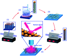
Fig. 1 shows the fabrication steps for Si nanowire–Au nanoparticle heterostructures as a novel substrate for SERS-based organic dye sensing. The following steps (1–5, Fig. 1) were involved: (1) growth of Si nanowires in the CVD approach, (2) wet-chemical synthesis and direct nucleation of Au nanoparticles on the Si nanowires, (3) dispersion of the as-produced Si nanowire–Au nanoparticle heterostructures on the surface-oxidized silicon substrate, (4) morphological evolution of Au nanoparticles on the Si nanowires in a controlled annealing process, and (5) correlation of heterostructure morphology with Raman signal enhancement effect for the organic molecules.
 |
| Fig. 1 Schematic representation of the process for fabricating Si nanowire–Au nanoparticle heterostructures and their application for SERS sensing. (1) CVD growth of Si nanowires, (2) direct and wet-chemical nucleation of Au nanoparticles on Si nanowires, (3) dispersion of the heterostructures on oxidized silicon substrate, (4) thermal annealing of heterostructures, and (5) SERS-based organic dye detection. | |
Growth of Si nanowires and their surface decoration with Au nanoparticles
Fig. 2A and B show the SEM images of the as-produced Si nanowires. Au nanoparticle was always found at the tip of each Si nanowire, indicating the growth was governed by well-known VLS mechanism.39 This growth process utilized sputtered and dewetted Au film on the Si substrate. The authors have thoroughly studied the dewetting of Au films to result in uniform dispersion of nanoparticles in their previous study.40 The resulting Au nanoparticles/islands were further served as the catalysts/seeds for the CVD growth of Si nanowires. The growth was conducted for 5 min and resulted in Si nanowires with a length of ∼8 to 12 μm, suggesting a nanowire growth speed of ∼27 to 40 nm s−1. The diameter of Si nanowires was observed to be consistent with the size of Au nanoparticle tips on the nanowires. From Fig. 2C, it can be estimated that the diameter of Si nanowire was ∼172.44 ± 90 nm. Fig. 2D–F shows the HRTEM images of the as-produced Si nanowires. A lattice spacing of ∼0.31 nm was observed for silicon (111) planes. Gold (111) planes with a lattice spacing of ∼0.23 nm was also observed for Au nanoparticle tips. The lattice structure of both gold and silicon present in the nanowires were further confirmed by the Fast Fourier Transform (FFT) image in the inset of Fig. 2F.
 |
| Fig. 2 (A and B) SEM images of the as-produced Si nanowires. (C) The diameter distribution (∼172.44 ± 90 nm) of Si nanowires. (D) TEM image of the as-produced Si nanowires. (E) HRTEM image indicating the lattice structure of the Si nanowire (marked as “1” in D). (F) HRTEM image indicating the lattice structure of the Au nanoparticle (catalyst/seed) at the tip of the Si nanowire (marked as “2” in D). Note: the average nanowire tip diameter is observed to be ∼154 ± 80 nm in (B). The inset in (F) show the corresponding FFT image for diffraction spots for silicon and gold. | |
As the next step, Si nanowires were decorated with extraneous Au nanoparticles in a wet-chemical nucleation process. This approach involves the chemical reduction of metal salt (HAuCl4) in presence of NaBH4, allowing for direct nucleation of Au nanoparticles on the Si nanowires. Fig. 3A–C show TEM images of the as-produced Si nanowire–Au nanoparticle heterostructures. Significant nanoparticle aggregation on nanowires was observed. The Au nanoparticles exhibited lattice spacing of ∼0.23 nm corresponding to the (111) planes. It is worthy to mention that this direct nucleation process has no significant damage on the structure of Si nanowires, as the silicon (111) crystal planes with a lattice spacing of ∼0.32 nm was also observed. XRD spectra of the as-produced Si nanowires and the Si nanowire–Au nanoparticle heterostructures further confirmed their crystal structure (Fig. 3D). Fig. 3E shows the estimation of size (average diameter ∼10.40 ± 3.59 nm) and inter-particle spacing (∼6.19 ± 2.30 nm) for the as-nucleated Au nanoparticles on the Si nanowires.
 |
| Fig. 3 (A–C) TEM images of the as-produced Si nanowire–Au nanoparticle heterostructures (before annealing). (D) XRD spectra of the as-produced Si nanowires and the Si nanowire–Au nanoparticle heterostructures before annealing. (E) Size and inter-particle spacing of the Au nanoparticle on Si nanowires. | |
Annealing of Si nanowire–Au nanoparticle heterostructures
In order to modulate the shape, size and surface distribution of Au nanoparticles on the Si nanowires, subsequent high-temperature annealing was conducted under various conditions including duration, temperature, and environment.41,42 The detailed experimental parameters can be found in Table S1 (ESI†). Fig. 4A–D show TEM images of the Si nanowire–Au nanoparticle heterostructures after annealing for various durations (15–120 min). As compared to the as-produced heterostructures (Fig. 3A and B), the distribution of Au nanoparticles is much more uniform and with minimized aggregation on the Si nanowires. HRTEM images of the heterostructures (Fig. 4E–H) show the lattice spacing for both silicon and gold. Detailed lattice analysis was further shown in Fig. S1 (ESI†). It could be observed that after the annealing process, the lattice spacing increased at the outer edge of the Au nanoparticle as compared to the inner core, resulting a core/shell nanoparticle configuration on the surface of Si nanowire. This could be attributed to the formation of gold silicide (AuSix) at the interface of Au nanoparticle and Si nanowire, which was growing into a shell structure with increasing annealing duration.43–45 As shown in Fig. 4E, 15 min annealing resulted in core/shell configuration of Au nanoparticles, where the core lattice spacing is observed to be ∼0.20 nm (corresponding to Au (200) plane) and the outer shell region (marked with dotted circle) exhibited lattice spacing of ∼0.22 nm. The shell thickness was observed to increase with annealing duration. When beyond 75 min, the whole nanoparticle exhibited a lattice spacing of ∼0.25 nm. This indicates that prolonged annealing duration (>75 min) resulted in complete phase transformation of Au nanoparticles into gold silicide nanoparticles. The details on kinetics of this transformation are discussed later.
 |
| Fig. 4 TEM images and lattice structure of the Si nanowire–Au nanoparticle heterostructures after annealing for (A and E) 15 min, (B and F) 45 min, (C and G) 75 min, and (D and H) 120 min. (I) Average diameter and inter-particle spacing of Au nanoparticles on Si nanowires after annealing for different durations. Contour graphs showing the distribution of Au nanoparticle (J) diameter and (K) spatial density as a function of the Si nanowire diameter and the annealing duration. Note: baseline annealing conditions were 625 °C in Ar environment. | |
It was observed that the diameter of Au nanoparticles on Si nanowires increased as a function of annealing duration from 15 min to 75 min (Fig. 4I, Table S2 in ESI†). The as-produced heterostructures exhibited an Au nanoparticles diameter of ∼10.4 nm, which was increased to ∼16.2 nm, 18.7 nm, and 22.6 nm after annealing for 15 min, 45 min, and 75 min, respectively. This increase can be explained by the Ostwald's ripening effect and surface migration of Au species, which resulted in growth of larger nanoparticle at the expense of smaller ones.40 However, when the annealing beyond 75 min, a sudden decrease in nanoparticle diameter (∼15 nm) is observed. It has been reported for annealing of Au/Si thin film structure, the silicide formation takes place at much lower temperatures than that used for the annealing.45 It is proposed that the possibility of Au diffusing towards Si or vice versa can lead to consumption of Au and result in shrinking of nanoparticle as observed in case of 120 min annealing. This further corroborates with the TEM observations that shows complete phase transformation of Au nanoparticles to gold silicide nanoparticles beyond 75 min of annealing. In regard to inter-particle spacing on Si nanowires, the as-produced heterostructures exhibited inter-particle spacing of ∼6.2 nm, which was increased to ∼10.1 nm after annealing of 15 min and remained nearly the same beyond this duration. This is an interesting observation as it suggests that surface migration of Au nanoparticles at the annealing conditions used was restricted and the process allowed for the formation of thermally-stable or sinter-resistant nanoparticle dispersion on Si nanowires. Similar observation have been reported for other one-dimensional heterostructures based on oxide nanowire–nanoparticle or carbon nanotube–nanoparticle systems.46–48
The microscopic observations were further utilized to develop contour maps correlating annealing duration and nanowire diameter with the nanoparticle diameter and spatial density (Fig. 4J and K). This uniquely shows that Si nanowires with large diameter favored the growth of nanoparticles, resulting in largest nanoparticles dispersed on the heterostructures. On the other hand, nanowires with small diameter allowed for greater nucleation of nanoparticles and thus, resulted in highest spatial density of the coated nanoparticles. Fig. 4J shows that annealing of 45 min resulted in largest nanoparticle diameters between ∼45–50 nm coated on surface of Si nanowires with largest diameters between ∼250–275 nm. This also suggests that higher the radius of curvature of nanowires, faster the surface migration of nanoparticles with enhanced Ostwald's ripening effect.49–51 Meanwhile, Si nanowires with small radius of curvature present higher surface energy,38 resulting in restricted surface migration and enhanced heterogeneous nucleation for the Au nanoparticles. Thus, the highest nanoparticle spatial density (9–11 × 1010 per cm2) region observed at the intersection of 75 min annealing duration and 50–100 nm diameter for Si nanowires (Fig. 4K).
The influence of annealing temperature on the morphology of Si nanowire–Au nanoparticle heterostructures was shown in Fig. 5A–D. Fig. 5E–H further show the corresponding HRTEM images. Annealing at 300 °C only resulted in slight morphology change (Fig. 5A) of the heterostructures as compared to the as-produced. Meanwhile, no obvious formation of gold/gold silicide core/shell nanoparticles was observed on this sample and the nanoparticle lattice spacing (∼0.23 nm) was similar to that of pristine Au nanoparticles (Fig. 5E). However, significantly improved Au nanoparticle uniformity was observed on the heterostructures annealed at 500 °C. The core/shell structure for the nanoparticles was also observed with the lattice spacing increased from ∼0.23 nm of the core to ∼0.25 nm of the shell (Fig. 5F). When the annealing temperature increased to 700 °C and 800 °C, the nanoparticles on the heterostructures show constant lattice spacing of ∼0.25 nm (Fig. 5G and H), indicating the phase transformation or gold diffusion process becomes more pronounced at high temperatures and the Au nanoparticles were completely converted to gold silicide. In addition, it needs to mention that annealing at 1000 °C led to the partially fusion of Si nanowires and severe destruction of the heterostructures was observed (Fig. S2, ESI†).
 |
| Fig. 5 TEM images and lattice structure of the Si nanowire–Au nanoparticle heterostructures after annealing at (A and E) 300 °C, (B and F) 500 °C, (C and G) 700 °C, and (D and H) 800 °C. (I) Average diameter and inter-particle spacing of Au nanoparticles on Si nanowires after annealing for different temperatures. Contour graphs showing the distribution of Au nanoparticle (J) diameter and (K) spatial density as a function of Si nanowire diameter and the annealing temperature. Note: baseline annealing conditions were 45 min duration and in Ar environment. | |
Fig. 5I further summarized the variation of size and inter-particle spacing of Au nanoparticles on the heterostructures after annealing at various temperatures (also see Table S2, ESI†). Annealing at 300 °C showed obvious influence on the distribution of Au nanoparticle size (even not much on the morphology as shown in Fig. 5A), which was increased from ∼10.4 nm of the as-nucleated (Fig. 3B) to ∼16.8 nm (Fig. 5A). Further increase the annealing temperature (from 500 °C to 800 °C) resulted in continuous increase of particle size. This is understandable since the diffusion efficiency of gold is increased at higher temperature, which is prone to the migration and merging of Au nanoparticles. The inter-particle spacing of Au nanoparticles increased from ∼6.19 nm (Fig. 3B) to ∼7.55 nm when annealed at 300 °C (Fig. 5A) and to ∼9.66 nm when annealed at 500 °C (Fig. 5B). Further increasing the temperature showed little effect on the inter-particle spacing, which kept a constant value of ∼10 nm (Fig. 5C and D). Fig. 5J and K show the correlation of particle size and spatial density with the annealing temperature and the diameter of Si nanowires. The largest Au nanoparticles were mainly distributed on the heterostructures with largest Si nanowire diameter and that treated at high temperature. This is due to the increase of gold migration rate on the low curvature nanowires (same as described above) and at high temperature.48 With this regard, one can understand that the highest spatial density of Au nanoparticles was mainly observed on the small-diameter nanowires and the heterostructures annealed in low temperatures (Fig. 5K).
TEM images of the Si nanowire–Au nanoparticle heterostructures annealed in various environments were shown in Fig. 6A–H. The aforementioned core/shell nanoparticles can be observed on the heterostructures that annealed in 5% O2/Ar and N2 environments (Fig. 6E and G). Meanwhile, the lattice spacing of nanoparticles on the heterostructures annealed in 10% H2/Ar and vacuum environment was increased from ∼0.23 nm of the pristine to ∼0.24 nm to ∼0.25 nm due to the formation of gold silicide. Fig. 6I further summarized the variation of particle diameter and inter-particle spacing of the heterostructures (see Table S2, ESI†). The heterostructures annealed in 5% O2/Ar environment show smaller average nanoparticle diameter (∼16.3 nm) as compared with that annealed in pure Ar (∼18.5 nm). This is because the outer layer of Si nanowires and Au nanoparticles was partially oxidized in the presence of O2. The oxide layers mitigated the direct diffusion of gold into Si nanowires as well as the surface migration of Au nanoparticles, leading to less changes in nanoparticle size during the annealing.52,53 The average diameter of nanoparticles after annealing in 5% H2/Ar was ∼16.8 nm (Fig. 6B and I). This relatively smaller size is due to the presence of hydrogen, which removed the pristine surface oxide layer on the Si nanowires and facilitated the diffusion of Au nanoparticles into Si nanowires.56 As a result, the surface migration and aggregation of Au nanoparticles was not significant. Moreover, annealing in vacuum also resulted in a less increased nanoparticle diameter (∼16.2 nm, Fig. 6D and I), which is probably due to the high diffusion rate of gold in silicon at low pressure.54 Heterostructures annealed in N2 environment (Fig. 6C and I) showed no significant difference on particle size and inter-particle spacing with that annealed in Ar.55 Contour images in Fig. 6J–K show the distribution of particle size and spatial density according to various environments and nanowire diameter. Similar with that observed in previous duration and temperature study, nanoparticles with the largest diameter were observed on large Si nanowires while the region with highest spatial density were observed on small nanowires. In addition, the region with highest spatial density was observed on heterostructures treated in the H2/Ar environment owning to the mitigation of surface migration and merging of Au nanoparticles in the presence of hydrogen.
 |
| Fig. 6 TEM images and lattice structure of the Si nanowire–Au nanoparticle heterostructures after annealing in various environments including (A and E) 5% O2/Ar, (B and F) 10% H2/Ar, (C and G) N2, and (D and H) vacuum. (I) Average diameter and inter-particle spacing of Au nanoparticles on Si nanowires after annealing for different environments. Contour graphs showing the distribution of Au nanoparticle (J) diameter and (K) spatial density as a function of Si nanowire diameter and the annealing environment. Note: baseline annealing conditions were 45 min duration and in Ar environment. | |
Histograms in Fig. S3 (ESI†) summarized the size distribution and inter-particle spacing distribution of Au nanoparticles on the heterostructures before and after annealing at various conditions. Composition analysis for the heterostructures before and after annealing (at 500 °C, 45 min and Ar environment) was conducted using STEM-mode EDS line profile. STEM images in Fig. S4A and B (ESI†) show different contrast of gold and silicon in the heterostructures, which were further identified by the EDS spectra in Fig. S4C and D (corresponding to spot “1” and “2” in Fig. S4B, see ESI†). Representative EDS line profiles of the nanowire heterostructures before and after annealing process is shown in Fig. S4E and F (ESI†). These line profiles clearly show the elements present and their maps as a function of location on the nanowire.
XPS study for the formation of gold silicide
TEM images (Fig. 4–6) clearly demonstrate a lattice spacing shift for nanoparticles on the heterostructures from ∼0.23 nm to ∼0.25 nm before and after annealing. This has been attributed to the formation of gold silicide according to the previous literatures.51–53 In order to make further quantitative conclusions, XPS was utilized to study the variation of chemical composition for the heterostructures annealed at various annealing conditions and further understand the surface migration/diffusion kinetics of Au nanoparticles on the Si nanowires. Wide-range XPS spectra and further deconvoluted Au 4f spectra were shown in Fig. S5–S7 (ESI†). Different elements such as Si, Au, O, C, and Na were observed for all the tested samples (Fig. S5A, S6A, and S7A, see ESI†). The existence of Na is due to NaBH4 used in the Au nanoparticle nucleation process.56 However, this peak was only observed on the as-produced nanowire heterostructures and was almost negligible after annealing. In addition, C and O are common contaminants resulting from the oxidized silicon substrate.
The peaks observed at ∼83.86 eV and ∼87.50 eV were assigned to Au 4f7/2 and Au 4f5/2 of metallic Au nanoparticles that nucleated on the Si nanowires (Fig. 7A).63 The further deconvolution fitting of this Au 4f spectrum shows nearly 100% pure metallic gold. This indicates that no gold oxide or Au3+ remaining on the heterostructures after Au nanoparticle nucleation. At the same time, the gold and silicon phases are chemically intact, which is consistent with the TEM images in Fig. 3A–C and EDS line profile in Fig. S4E (ESI†). The Au 4f spectrum for the heterostructures annealed for 15 min (corresponding to sample #1 in Table S1, see ESI†) was shown in Fig. 7B. The deconvolution resulted in two additional peaks in high binding energy region (∼84.43 eV and ∼88.55 eV) and the peak area of metallic gold (at ∼86.65 eV and ∼87.68 eV) became relatively small. The emergence of these two peaks was also observed and attributed to the chemical reaction of gold and silicon atoms owning to the formation of gold silicide.57–59 This observation is consistent with the core/shell nanoparticles observed in the TEM image (Fig. 4E) and confirms gold silicide formation. The same phenomenon was observed on the spectrum obtained on the heterostructures annealed for 45 min (Fig. 7C, corresponding to sample #2 in Table S1, see ESI†). Further decreased peak area for metallic gold (at ∼83.53 eV and ∼87.68 eV) was observed on this sample. After annealing the heterostructure for 75 min (Fig. S5E, sample #3†) and 120 min (Fig. S5F, sample #4†), no peaks for the metallic gold was observed in the deconvoluted spectra. This further confirmed the lattice variation observed in Fig. 4G and H since no metallic gold core was observed on these heterostructures (sample #3 and #4 in Table S1, see ESI†).
 |
| Fig. 7 (A–C) Deconoluted XPS spectra (Au 4f) of the Si nanowire–Au nanoparticle heterostructures (A) before and after annealing for (B) 15 min and (C) 45 min. (D) Schematic showing the formation of gold silicide (AuSix) shell on Au nanoparticles and the geometrical model for the XPS analysis. (E) Variation of AuSix shell thickness as a function of annealing duration at different temperature. (E) Linear plot showing the relationship between the diffusion coefficient and temperature for the AuSix formation activation energy calculation. | |
Since XPS is a surface characterization technique with the detection depth of ∼8 nm,63 and meanwhile the diameter of Au nanoparticles on the annealed heterostructures was varying from ∼15 nm to ∼20 nm (see Table S3, ESI†), the metallic gold detected by the photoelectrons will be only from part of the nanoparticles. Thus, it is necessary to establish a theoretical model to calculate the accurate molar fraction of metallic gold and thickness of the gold silicide shell. This will also lead to further understanding on the kinetics of the gold silicide formation process. The model was schematically shown in Fig. 7D. Here we assume the nanoparticles on Si nanowires are spherical and composed of a concentric gold core and gold silicide shell. The incident X-ray is from the top of the core/shell structure with a penetrating depth of 8 nm. Accordingly, one can realize that the molar fraction (FAu) directly calculated by the area ratio from the XPS spectra is only for the spherical cap in Fig. 7D (photoelectron region). The volume of this spherical cap (V) being detected by XPS was given by
|
 | (1) |
where
R is the outside radius of the core/shell structure,
H is the photoelectron emission depth and was assumed to be 8 nm. Thus, according to
Fig. 7D,
FAu calculated from the area ratio of XPS spectra can be written as
|
 | (2) |
where
r represents the radius of the metallic gold core. It needs to mention here that
eqn (2) is only suitable for the core/shell nanoparticles with
R −
r ≥
H (these show metallic gold peaks in XPS spectra). Furthermore, knowing
FAu from the XPS spectra, the real molar fraction (
FAu, real) of the core/shell nanoparticles can be calculated by
The obtained molar fraction values were summarized in Table S3 (see ESI†). It has been reported that diffusion of silicon atoms in the gold at the elevated temperature is a thermodynamically feasible process due to its high solubility in gold and the low eutectic temperature of gold and silicon (∼363 °C).39 It can be observed that annealing the heterostructures at 625 °C for 15 min resulted in a metallic gold content of 19.23% (sample #1, Table S3, see ESI†). When the annealing was conducted for 45 min, the remaining metallic gold is 4.10%.
XPS spectra of Au 4f for the nanowire heterostructures annealed at various temperatures and environments (sample #5–#13) were also deconvoluted and shown in Fig. S6 and S7 (see ESI†). The peak locations were further summarized in Table S3 (ESI†). For all these annealed samples, two addition gold silicide peaks were observed in the positive direction (with a binding energy shift of ∼1 eV compared to the metallic gold). Metallic gold peaks were only observed on heterostructures annealed at 300 °C and 500 °C, but not on these annealed at 700 °C, 800 °C and 1000 °C. This is because the diffusion rate of silicon in gold is much higher at high temperature, resulting complete phase transformation from gold to gold silicide. In the environment set, we observed the metallic gold peaks on the heterostructures annealed in Ar, N2, and 5% O2/Ar but not on the samples annealed in 5% H2/Ar and vacuum environments. This is consistent with the TEM observations in Fig. 6 and further confirmed above reasoning that the presence of hydrogen or low pressure facilitated the diffusion and alloying of silicon and gold.
Kinetics for the formation of gold silicide
Considering that the formation of gold/gold silicide core/shell nanoparticles on the heterostructures during the annealing fundamentally involves the diffusion of Si atoms in Au nanoparticles, one can apply the Fick's second law (eqn (4)) to this process and further study the formation kinetics of gold silicide. |
 | (4) |
where c is the concentration of Si in Au nanoparticles, t is the time and D is the chemical interdiffusion coefficiency and only depends on temperature. Solving eqn (4) with the following boundary conditions: c = c0 at t = 0 and c = cs at x = 0, we can get: |
 | (5) |
where x can be considered as the thickness of gold silicide shell, (x = R − r, the values for various samples were shown in Table S3, see ESI†), erf is the Gauss error function and can be express as
. Further consider c(x, t) = cs, the following equation can be obtained, |
 | (6) |
Accordingly, we were able to calculate D at various temperatures according to the slopes of x ∼ t1/2 plots (Fig. 7E).60,61 These linear plots further indicate that the formation of AuSix is controlled by the Si diffusion process and thus the following Arrhenius equation can be used to describe the activation energy (Ea) of this diffusion process.62
|
 | (7) |
where
T is the temperature,
D0 is pre-exponential factor and
k is the Boltzmann's constant. The plot of ln
D(
T) ∼ 1/
T was further shown in
Fig. 7F and the calculated activation energy is 1.23 eV. This value is slightly lower than the previously calculated activation energy for the formation of platinum silicide,
60–62 which can be explained by the high solubility of silicon atoms in gold.
Surface-enhanced Raman scattering (SERS) effect
Controlled annealing of the heterostructures resulted in uniform dispersion of Au nanoparticles on the Si nanowires with specific size, inter-particle spacing and density, which further opens a great opportunity for reproductive and sensitive organic detection based on the Surface-enhanced Raman scattering (SERS). Various heterostructure samples as shown in Table S1 (ESI†) were dispersed on the oxidized silicon substrate. This was followed by anchoring R6G molecules on the heterostructures as Raman probe. As shown in Fig. 8A, Raman tests were conducted at various locations along the heterostructures to evaluate their reproducibility and sensitivity. Fig. 8B further shows the representative optical image of the heterostructures dispersed on the oxidized silicon substrate. The colored spots marked on the nanowire heterostructure represents various locations for Raman test. The resulting Raman signal intensity (estimated for Raman peak of R6G at ∼1360 cm−1) for the as-produced Si nanowires, Si nanowire–Au nanoparticle heterostructures before and after annealing at different duration were shown in Fig. 8C. The columns with different colors for each sample are corresponding to the spots marked in Fig. 8B. The same test were conducted on ten nanowires for each sample to evaluate the Raman detection sensitivity. The average intensity values for all the tested spots on these nanowires/heterostructures were summarized in Fig. 8D.
 |
| Fig. 8 (A) Schematic showing the collection of Raman signal along the Si nanowire–Au nanoparticle heterostructures. (B) Optical images of the heterostructures and corresponding spots for the Raman measurement. (C) Intensity of Raman signal for R6G at various spots along the Si nanowires or Si nanowire–Au nanoparticle heterostructures. (D) Average Raman intensity for various samples corresponding to (C). (E) Representative Raman spectra of R6G collected on samples corresponding to (C). The same Raman test was conducted on samples in the temperature and environment study and the results were shown in (F–H, temperature set) and (I–K, environment set). Note: the Raman intensity was evaluated using the peak located at ∼1360 cm−1. The average intensity in D, G and J was calculated by collecting Raman signal from ten heterostructures. | |
Representative Raman spectra of R6G for various samples were further shown in Fig. 8E. No signal of R6G was observed on the blank substrate (without any nanowire heterostructure), indicating the substrate is nearly insensitive for this Raman probe molecules. The as-produced Si nanowires show weak signals for R6G while the signals on the as-produced Si nanowire–Au nanoparticle heterostructures were significantly increased. As described above, such Raman enhancement has been attributed to the presence of localized surface plasmon resonance (LSPR) on Au nanoparticles.3–6 The heterostructures annealed at 625 °C for 15 min (sample #1) and 45 min (sample #2) show further enhanced Raman signal of R6G due to the reconfiguration (size, inter-particle spacing, and density, see Fig. 4) of surface nanoparticles. However, the Raman signals on the heterostructures annealed for 75 min (sample #3) and 120 min (sample #4) were decreased as compared with that for 45 min. This can be attributed to the increase of inter-particle spacing (Fig. 4I) and decrease of particle density (Fig. 4K) on the Si nanowires. Another possible reason is that after annealing for a long duration (>45 min), most of these Au nanoparticles have been converted to gold silicide and the Au core was nearly disappeared. This may lead to the insensitivity for R6G due to the weakening of the LSPR on the surface of gold silicide nanoparticles.
The same Raman tests were also conducted on the Si nanowire–Au nanoparticle heterostructures annealed at various temperatures and environments (sample #5–#13, Table S2, ESI†). The heterostructures (sample #5) annealed at 300 °C show no obvious enhancement of Raman signal since the size and inter-particle spacing of this sample (Fig. 5A and I) was not significantly changed as compared with the as-produced heterostructures. The highest Raman enhancement was observed on the heterostructures annealed at 500 °C. This is consistent with that observed in Fig. 5K, where the highest particle density was observed on the sample annealed at this temperature. These closely located nanoparticles have high possibility to overlap their surface electrical field, which will significantly enhance the Raman spectra of the anchored molecules.63 The heterostructures annealed at 700 °C and 800 °C show weakened Raman signals than these annealed at 500 °C and 625 °C. This is because the diffusion of silicon in gold nanoparticles was facilitated at high annealing temperature (>700 °C) and most of the particles have converted to silicide.
The heterostructures annealed in the oxygen and hydrogen environments show weak enhancement on the Raman signal while these annealed in inert environments (Ar, N2, and vacuum) show significant signal improvement (Fig. 8I). These observations can be explained by the particle configuration (size, inter-particle spacing, and density) showing in Fig. 6. The heterostructures annealed in oxygen environment resulted in formation of surface SiO2 and this might shadow the surface plasmon resonance effect of Au nanoparticles.64 For the heterostructures annealed in the hydrogen environment, the existence of H2 facilitated the diffusion between gold and silicon, resulting Au nanoparticles partially diffused into the Si nanowires. As a result, the particle size becomes small and the Raman enhancement was not significant. The heterostructures annealed in N2 environment show similar enhancement with that annealed in the Ar environment. Further improved Raman enhancement was observed on these heterostructures annealed in the vacuum environment. This can be attributed to the relatively small inter-particle spacing of surface nanoparticles that formed during the annealing at low pressure.
Conclusions
In this paper, we report a facile approach for the fabrication of Si nanowire–Au nanoparticle heterostructures using a wet-chemical nucleation – annealing approach. The surface migration behaviors (including variation of chemical composition and phase transformation kinetics) of Au nanoparticles on the Si nanowire during annealing were further studied in detail. The results indicate that the surface dispersion (size, inter-particle spacing and spatial density) of Au nanoparticles has a significant dependence on the annealing conditions including duration, temperature and environment. TEM and XPS study further show that such high temperature annealing led to significant migration/diffusion of Au nanoparticles and further resulted in the formation of gold silicide in the nanoparticles. Kinetics analysis indicates that this silicide formation process was controlled by the diffusion of silicon atoms in Au nanoparticles. The activation energy for this process is ∼1.23 eV. For the SERS-based organic detection, Raman enhancement showed a significant dependence on the distribution and chemical state of Au nanoparticles on the heterostructures. Highest Raman enhancement was observed on the heterostructures annealed at 500 °C in Ar for 45 min. This study provides fundamental knowledge on the surface migration and diffusion behavior of Au nanoparticles on Si nanowire at high temperature process and leads to reliable guidance for future development of SERS-based chemical sensors.
Acknowledgements
This work was supported by National Science Foundation (Award #: 0925445) and NSF-EPSCoR-RII award. The authors thank the University of Alabama's Office of sponsored programs and Research Grant Committee Award for additional support for this research. The authors thank the Central Analytical Facility (CAF).
Notes and references
- X. Gong, Y. Bao, C. Qiu and C. Jiang, Chem. Commun., 2012, 48, 7003 RSC.
- B. Zhang, H. Wang, L. Lu, K. Ai, G. Zhang and X. Cheng, Adv. Funct. Mater., 2008, 18, 2348 CrossRef CAS PubMed.
- P. Luo, C. Li and G. Shi, Phys. Chem. Chem. Phys., 2012, 14, 7360 RSC.
- J. P. Camden, J. A. Dieringer, J. Zhao and R. P. Van Duyne, Acc. Chem. Res., 2008, 41, 1653 CrossRef CAS PubMed.
- Z. Q. Tian, B. Ren, J. F. Li and Z. L. Yang, Chem. Commun., 2007, 34, 3514 RSC.
- H. Ko, S. Singamaneni and V. V. Tsukruk, Small, 2008, 4, 1576 CrossRef CAS PubMed.
- R. Gunawidjaja, E. Kharlampieva, I. Choi and V. V. Tsukruk, Small, 2009, 5, 2460 CrossRef CAS PubMed.
- N. J. Halas, S. Lal, S. Link, W. S. Chang, D. Natelson, J. H. Hafner and P. Nordlander, Adv. Mater., 2012, 24, 4842–4877 CrossRef CAS PubMed.
- X. M. Lin, Y. Cui, Y. H. Xu, B. Ren and Z. Q. Tian, Anal. Bioanal. Chem., 2009, 394, 1729 CrossRef CAS PubMed.
- M. Fan, G. F. Andrade and A. G. Brolo, Anal. Chim. Acta, 2011, 693, 7–25 CrossRef CAS PubMed.
- M. W. Shao, M. L. Zhang, N. B. Wong, D. D. D. Ma, H. Wang, W. Chen and S. T. Lee, Appl. Phys. Lett., 2008, 93, 233118 CrossRef PubMed.
- S. Deng, H. M. Fan, X. Zhang, K. P. Loh, C. L. Cheng, C. H. Sow and Y. L. Foo, Nanotechnology, 2009, 20, 175705 CrossRef CAS PubMed.
- C. Fang, A. Agarwal, E. Widjaja, M. V. Garland, S. M. Wong, L. Linn and N. Balasubramanian, Chem. Mater., 2009, 21, 3542 CrossRef CAS.
- K. Q. Peng and S. T. Lee, Adv. Mater., 2011, 23, 198 CrossRef CAS PubMed.
- Y. Li and N. Chopra, MRS Proceedings, 2013, 1572, mrss13-1572 CrossRef.
- M. Lv, S. Su, Y. He, Q. Huang, W. Hu, D. Li and S. T. Lee, Adv. Mater., 2010, 22, 5463 CrossRef CAS PubMed.
- K. Q. Peng, X. Wang, X. L. Wu and S. T. Lee, Nano Lett., 2009, 9, 3704 CrossRef CAS PubMed.
- M. W. Shao, Y. Y. Shan, N. B. Wong and S. T. Lee, Adv. Funct. Mater., 2005, 15, 1478 CrossRef CAS PubMed.
- F. Zhao, D. D. Zhao, S. L. Wu, G. A. Cheng and R. T. Zheng, Surf. Coat. Technol., 2013, 228, S349 CrossRef CAS PubMed.
- F. Zhang, T. Song and B. Sun, Nanotechnology, 2012, 23, 194006 CrossRef PubMed.
- B. Eisenhawer, S. Sensfuss, V. Sivakov, M. Pietsch, G. Andrä and F. Falk, Nanotechnology, 2011, 22, 315401 CrossRef CAS PubMed.
- Z. Peng, H. Hu, M. I. B. Utama, L. M. Wong, K. Ghosh, R. Chen and Q. Xiong, Nano Lett., 2010, 10, 3940 CrossRef CAS PubMed.
- Y. Li, J. C. Dykes and N. Chopra, MRS Online Proc. Libr., 2013, 1551, mrss13-1551 Search PubMed.
- Y. He, S. Su, T. Xu, Y. Zhong, J. A. Zapien, J. Li and S. T. Lee, Nano Today, 2011, 6, 122 CrossRef CAS PubMed.
- H. Wang, X. Jiang, S. T. Lee and Y. He, Small, 2014, 10, 4455 CrossRef CAS PubMed.
- X. Wang, W. Shi, G. She and L. Mu, J. Am. Chem. Soc., 2011, 133, 16518 CrossRef CAS PubMed.
- M. Shao, L. Cheng, X. Zhang, D. D. D. Ma and S. T. Lee, J. Am. Chem. Soc., 2009, 131, 17738 CrossRef CAS PubMed.
- Y. Li, W. Shi, J. C. Dykes and N. Chopra, MRS Proceedings, 2013, 1547, 103 CrossRef.
- E. Galopin, J. Barbillat, Y. Coffinier, S. Szunerits, G. Patriarche and R. Boukherroub, ACS Appl. Mater. Interfaces, 2009, 1, 1396 CAS.
- M. S. Schmidt, J. Hübner and A. Boisen, Adv. Mater., 2012, 24, 11 Search PubMed.
- M. Hu, F. S. Ou, W. Wu, I. Naumov, X. Li, A. M. Bratkovsky and Z. Li, J. Am. Chem. Soc., 2010, 132, 12820 CrossRef CAS PubMed.
- S. H. Christiansen, M. Becker, S. Fahlbusch, J. Michler, V. Sivakov, G. Andrä and R. Geiger, Nanotechnology, 2007, 18, 035503 CrossRef CAS PubMed.
- S. Y. Baik, Y. J. Cho, Y. R. Lim, H. S. Im, D. M. Jang, Y. Myung and H. S. Kang, ACS Nano, 2012, 6, 2459 CrossRef CAS PubMed.
- R. Chen, D. Li, H. Hu, Y. Zhao, Y. Wang, N. Wong and Q. Xiong, J. Phys. Chem. C, 2012, 116, 4416 CAS.
- C. P. Li, X. H. Sun, N. B. Wong, C. S. Lee, S. T. Lee and B. K. Teo, J. Phys. Chem. B, 2002, 106, 6980 CrossRef CAS.
- S. Y. Sayed, J. Buriak, D. Wang, F. Wang, P. Li and M. Malac, CrystEngComm, 2012, 14, 5230 RSC.
- S. Y. Sayed, F. Wang, M. Malac, A. Meldrum, R. F. Egerton and J. M. Buriak, ACS Nano, 2009, 3, 2809 CrossRef CAS PubMed.
- J. B. Hannon, S. Kodambaka, F. M. Ross and R. M. Tromp, Nature, 2006, 440, 69 CrossRef CAS PubMed.
- V. Schmidt, J. V. Wittemann, S. Senz and U. Gösele, Adv. Mater., 2009, 21, 2681 CrossRef CAS PubMed.
- N. Chopra, J. Wu and L. Summerville, Carbon, 2013, 62, 76 CrossRef CAS PubMed.
- Y. Li and N. Chopra, Phys. Chem. Chem. Phys., 2015, 17, 12881 RSC.
- Y. Li and N. Chopra, Appl. Surf. Sci., 2015, 344, 27 CrossRef CAS PubMed.
- S. Chakraborty, J. Kamila, B. Rout, B. Satpati, P. V. Satyam, B. Sundaravel and B. N. Dev, Surf. Sci., 2004, 549, 149 CrossRef CAS PubMed.
- L. J. Chen, JOM, 2005, 57, 24 CrossRef CAS PubMed.
- U. M. Bhatta, A. Rath, J. K. Dash, J. Ghatak, L. Yi-Feng, C. P. Liu and P. V. Satyam, Nanotechnology, 2009, 20, 465601 CrossRef PubMed.
- Y. Li, K. Kumar and N. Chopra, Nanomater. Energy, 2014, 3, 93 CrossRef.
- Y. Li and N. Chopra, MRS Proceedings, 2013, 1543, 119 CrossRef.
- N. Chopra, Y. Li and K. Kumar, MRS Proceedings, 2014, 1675, mrss14 CrossRef.
- T. Kawashima, T. Mizutani, T. Nakagawa, H. Torii, T. Saitoh, K. Komori and M. Fujii, Nano Lett., 2008, 8, 362 CrossRef CAS PubMed.
- Y. Wan, Y. Wang, B. Chen, Y. Fang and J. Sha, Phys. Status Solidi C, 2009, 6, 687 CrossRef CAS PubMed.
- V. A. Sivakov, R. Scholz, F. Syrowatka, F. Falk, U. Gösele and S. H. Christiansen, Nanotechnology, 2009, 20, 405607 CrossRef CAS PubMed.
- T. Xie, V. Schmidt, E. Pippel, S. Senz and U. Gösele, Small, 2008, 4, 64 CrossRef CAS PubMed.
- W. Lerch and N. A. Stolwijk, J. Appl. Phys., 1998, 83, 1312 CrossRef CAS PubMed.
- M. A. Nicolet, Thin Solid Films, 1978, 52, 415 CrossRef CAS.
- G. J. Sprokel and J. M. Fairfield, J. Electrochem. Soc., 1965, 112, 200 CrossRef CAS PubMed.
- J. Wu, W. Shi and N. Chopra, J. Phys. Chem. C, 2012, 116, 12861 CAS.
- B. Sundaravel, K. Sekar, G. Kuri, P. V. Satyam, B. N. Dev, S. Bera and F. Caccavale, Appl. Surf. Sci., 1999, 137, 103 CrossRef CAS.
- R. Khalfaoui, C. Benazzouz, A. Guittoum, N. Tabet and S. Tobbeche, Vacuum, 2006, 81, 45 CrossRef CAS PubMed.
- D. K. Sarkar, S. Bera, S. Dhara, K. G. M. Nair, S. V. Narasimhan and S. Chowdhury, Appl. Surf. Sci., 1997, 120, 159 CrossRef CAS.
- A. K. Pant, S. P. Murarka, C. Shepard and W. Lanford, J. Appl. Phys., 1992, 72, 1833 CrossRef CAS PubMed.
- M. Wittmer, J. Appl. Phys., 1983, 54, 5081 CrossRef CAS PubMed.
- J. M. Poate and T. C. Tisone, Appl. Phys. Lett., 2003, 24, 391 CrossRef PubMed.
- N. J. Halas, S. Lal, S. Link, W. S. Chang, D. Natelson, J. H. Hafner and P. Nordlander, Adv. Mater., 2012, 24, 4842 CrossRef CAS PubMed.
- I. Al-Ogaidi, H. Gou, A. K. Al-kazaz, Z. P. Aguilar, A. K. Melconian, P. Zheng and N. Wu, Anal. Chim. Acta, 2014, 811, 76 CrossRef CAS PubMed.
Footnote |
† Electronic supplementary information (ESI) available. See DOI: 10.1039/c5ra06921a |
|
This journal is © The Royal Society of Chemistry 2015 |
Click here to see how this site uses Cookies. View our privacy policy here.