DOI:
10.1039/C5RA06102D
(Paper)
RSC Adv., 2015,
5, 52235-52242
Single-source mediated facile electrosynthesis of p-Cu2S thin films on TCO (SnO2:F) with enhanced photocatalytic activities†
Received
6th April 2015
, Accepted 4th June 2015
First published on 5th June 2015
Abstract
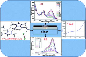
Electrosynthesis of p-Cu2S thin films on a fluorine-doped tin oxide coated transparent conducting TCO (SnO2:F) glass substrate is carried out by chronoamperometry and cyclic voltammetry (CV) using an ethanolic solution of a single-source precursor (SP), [Cu(mdpa)2][CuCl2] (where mdpa is 3,5-dimethyl pyrazole-1-dithioic acid). The appropriate potential at which the formation of stoichiometric p-Cu2S thin films occurs was found to be −0.48 V. The mechanism of the selective deposition of the p-Cu2S phase can be described by the electroreduction of Cu–N/S bonds in the coordination sphere following the dissociation of a precursor complex into Cu+ and mdpa. The free ligand mdpa is reduced to sulfide ion producing volatile organics in the electrochemical process. The quality deposition of thin films depends on the optimization of the SP concentration. An X-ray diffraction study reveals the high chalcosite phase of copper sulfide with preferential orientation along the (110) plane. The I–V characteristic of the as deposited Cu2S/TCO thin film shows a non-ohmic behavior suggesting the formation of a p–n heterojunction diode. The p-Cu2S/TCO thin films are found to be excellent photocatalysts for the photo-degradation of Congo Red (CR) under visible light irradiation. It has also been shown that the photocatalytic activity of the deposited thin films increased many fold with the addition of a catalytic amount of hydrogen peroxide in the photo-degradation of Rose Bengal (RB) dye under visible light irradiation. A possible mechanism for the improved photoactivity of p-Cu2S/TCO is proposed and involves the electron scavenging property of H2O2 followed by OH− radical formation, significantly accelerating the photodegradation of RB dye.
1. Introduction
Metal chalcogenides have received tremendous interest because of their various applications in optoelectronics devices,1 solar cells,2,3 Light emitting diodes,4,5 cathodic materials in lithium rechargeable batteries6,7 and photoelectrochemical cells.8 CuxS (1 ≤ x ≤ 2) is one important class of semiconducting materials with very different electrical and optical properties depending on the exact composition. The prominent and distinct phases of copper sulfide are chalcocite (Cu2S), djurleite (Cu1.96S), annilite (Cu1.75S) and covellite (CuS) at room temperature.9 It has been proved that the compounds exhibit a p-type semiconductor character with copper vacancy defects as acceptors and the photocurrent observed is increased with the increase of the x value in CuxS. The band gap of copper sulfide can vary in a wider range (1.2 to 2.5 eV) with stoichiometric composition, which makes it a highly desirable material for solar cells,10,11 nonvolatile memory devices,12 nano-scale switches,13 lithium ion batteries,14 gas sensing15,16 and theranostic applications.16 Cu2S can also be used as an ideal light absorber in extremely thin absorber (ETA) solar cells due to non-toxicity, low cost, abundance, and good absorption characteristics.17
In literature, various methods are reported to synthesize CuxS which include chemical vapor deposition (CVD),18 ultrasonic spray pyrolysis,19 chemical bath deposition (CBD),20 reactive evaporation,21 RF sputtering22 and electrochemical processes.23 Among these the electrochemical synthesis of nanomaterials and thin films could be a cost effective technology for the production of photoelectrochemical cell. These film based on photovoltaic technologies are being developed as a means of substantially reducing the cost of PV-system. The rationale for this is that thin films modules are expected to be cheaper in manufacture owing to their low materials cost, energy consumption and handling cost. Several techniques have been reported for the synthesis of copper sulfide nanostructured thin films and materials. The electroless chemical deposition of thin films of Cu2S, Cu1.8S, Cu1.4S, and CuS on glass, polyester, and metal substrates from aqueous copper thiosulfate in acidic medium was reported by Grozdanov.24 Elsewhere, spray pyrolysis deposition from aqueous solution containing CuCl2, thiourea (TU), and cationic surfactant has been used for CuS thin film fabrication.25 There are very few reports on electrochemical synthesis of copper sulfide nanostructures. Yang and Hu26 synthesized CuS nanoparticles using a copper electrode as a sacrificial anode in a Na2S2O3 and thioglycerol aqueous solution at a constant potential of 0.5 V. Yang and Hu also noticed that the production of OH− at the cathode facilitated the reaction between Cu2+ and dissolved sulfur species. Lai et al.27 have reported the template-assisted electrochemical synthesis of Cu2S nanowires where copper deposition occurred into the pores of an anodic aluminum oxide. Afterward, the template was removed and vapor (H2S) sulfidation of copper nanowires produced Cu2S nanowires. In an another report,28 fabrication of CuS nanowire was done by AC electrodeposition from aqueous solutions of dimethylsulfoxide solution containing copper chloride and elemental sulfur into anodic aluminum oxide templates. Ghahremaninezhad29 reported electrosynthesis of copper sulfide nanowires from a mixture of dilute Cu2+ solution and thiourea complexing agent. The Cu2S thin films deposition on a substrate was reported following thermal co-evaporation of the elemental constituents.30 Ricardo Cordova et al. reported the electrosynthesis and electrochemical characterization of a thin phase of CuxS (x → 2) on ITO electrode.31 In an another report, cathodic electrodeposition of Cu2S thin films was performed on Ti-substrate by K. Anuar et al.32 T. Mahalingam reported cathodic deposition of copper sulfides thin films of onto ITO substrate potentiostatically under various bath temperatures and deposition potentials.33 In an another report, cyclic voltammetry (0.10 to 1.50 V) method is used to synthesize Cu2S nanoparticles in the presence of polyvinylalcohol as stabilizer.34 However, the electrochemical deposition of copper sulfide thin films using only single-source precursor solution without using any external surfactants and/or stabilizers is still not found in literature though the uses of single-source precursors have some key advantages over the other conventional methods for preparing inorganic powders, nanoparticles, and thin films. Here, we report for the first time the electrosynthesis of Cu2S nanostructured thin films from a SP solution. Mostly, the single-source precursors are metal–organic or organo-metallic compounds which have century long advanced science and the ease of synthesis of SPs in ambient conditions popularizes the use of it in preparation of semiconductor chalcogenides.35,36 The protocol of single-source route is based on the advantages of mildness, safety and simplified one-pot synthesis of nanocrystals.37 Lastly, the presence of all constituent elements in required atomic ratios is chemically maintained in a SP strategy, which offers a clean synthetic method to produce pure compounds.38,39 Use of SP in the electrochemical method might be relatively inexpensive, scalable and easily controllable in making films and particles with desire thickness. Here, we demonstrate the SP mediated electrosynthesis of p-type Cu2S thin films without using any external stabilizing agents and checked the photocatalytic activities towards the degradation of CR and RB dyes in visible light.
2. Experimental
2.1. Synthesis of SP, [Cu(mdpc)2][CuCl2]
The synthesis of ligand, methyl ester of 3,5-dimethyl pyrazole-1-carbodithioc acid (mdpa) was carried out following a method.40 In brief, the SP was synthesized by mixing of a 20 mL ethanolic solution of CuCl2, 2H2O (10 mmol, 1.70 g) and a 20 mL ethanolic solution of methyl ester of 3,5-dimethyl pyrazole-1-carbodithioc acid (mdpa) (10 mmol, 1.86 g) with constant stirring. Stirring is continued for half an hour where a deep blue compound separated out. The precipitate formed was filtered, washed with excess ethanol and dried in an oven at 90 °C.
2.2. Deposition of Cu2S thin film
The film deposition was carried out in a three electrode system using an electrochemical workstation of CH Instruments (600 D Series) applying Cyclic voltammetry (CV) and chronoamperometry (CA) technique. First TCO glass of 3 × 1 cm2 was cleaned with boiling methanol then ultrasonicated for 5 minutes. The properly cleaned TCO glass substrate was taken as the working electrode, a Pt foil and a saturated Ag–AgCl electrode were served as the counter and reference electrodes, respectively and all are vertically clamped in a chemical bath containing 40 mL 0.017 M SP and 10 mL 0.01 M KCl (as supporting electrolyte). The total volume of the solution was maintained to 50 mL with deionized water. The TCO served as the cathode. The electrodes were short-circuited externally through a copper wire. The deposition was carried out at room temperature i.e., 25 °C without stirring the solution. Electrical characterization was carried out using DC I–V measurements. The DC voltage was applied along the thickness of the films using a KITHLEY 4200 instrument. Graphite was used as contact both with Cu2S and TCO (SnO2:F) (highly conducting materials) keeping the area of contacts (ca. 0.20 cm2). Photographs of films are given in ESI (Fig. S1†).
2.3. Characterization
UV-Visible absorption spectra of the samples were recorded on a Perkin Elmer Lambda 35 spectrophotometer in the wavelength range region 200–800 nm at room temperature. X-ray diffraction (XRD) of the films were recorded using a Seifert XDAL 3000 diffractometer using graphite-monochromated Cu-Kα radiation (λ = 1.54 Å) with a scan rate 5° min−1 over a range of 5° < 2θ < 80° with steps of 0.02° and scintillation detector is operating at 40 kV and 40 mA. The FESEM of thin films were analyzed with a JEOL JSM7600F (FESEM) field emission scanning electron microscope (FESEM) with 20 kV accelerating voltage. Energy dispersive X-ray (EDX) analysis of the sample was carried out on Oxford instrument INCA attached to the SEM in the scanning range of 20 keV. Photocatalytic activity of Cu2S/TCO was studied with a 50 mL of 0.9 × 10⁻⁴ and 1.5 × 10⁻⁵ M aqueous solution of CR and RB, respectively in a 100 mL beaker using visible light source. A 250 W indoor fluorescent lamp was used as light source. To test the photocatalytic degradation of CR, a solution of known CR concentration and photocatalyst (Cu2S/TCO and Cu2S NCs) was allowed getting adsorption equilibrium for 120 min in the darkness. Then the solution was exposed to visible light irradiation under magnetic stirring. At 10 min interval, 3 mL of solution and/or suspension was sampled and centrifuged to remove the photocatalyst films/powders. The concentration of the dye after photocatalytic degradation was determined with a UV-Vis spectrophotometer (Perkin Elmer Lambda 35).
3. Results and discussion
Single-source precursor (SP), [Cu(mdpa)2][CuCl2] (where mdpa is 3,5-dimethyl pyrazole-1-dithioic acid) was synthesized and structurally characterized (Fig. S2†) by us and it was used to synthesize in the selective synthesis of higher chalcosite (Cu2S).40 The details of the mdpa and SP syntheses and their characterizations were done earlier by us40 through available instruments. The out of plane position of the two adjacent pyrazole rings leads to less steric crowding among two methyl group at 3 and 5 positions (see ESI, Tables S1 to S4†). The overall distorted tetrahedral structure of the SP makes it vulnerable to ligand substitution prior to formation of Cu2S. The complex also easily undergoes into the alcohol which is essential for electrolytic synthesis. The fair solubility and the structural feature of SP prompt us to use it as electrolyte in electrodeposition of Cu2S onto TCO.
3.1. Electrodeposition
3.1.1 Cyclovoltammetry. The cyclovoltammetry (CV) and chronoamperometry (CA) are used to study the behavior of SP in electrochemical depositions.41 CV studies were carried out in a standard three electrode cell using a potentiostat and a data acquisition system. The CV experiments were performed using an aqueous ethanolic solution comprising of certain amount of dried SP (MW 570) in 40 mL methanol and 10 mL 0.05 M KCl as supporting electrolyte. Electrolyte solutions containing 0.008, 0.017 and 0.026 M of SP were prepared for electrodeposition. Cyclic voltammograms of Cu2S thin films deposition with different molar concentration of SP are shown in Fig. 1. All experiments were performed under constant temperature (25 °C) at pH 4 without using any stabilizing/complexing agents. Electrochemical setup was a standard three-electrode cell comprising TCO glass substrate as working electrode, a Pt foil as counter electrode and a saturated Ag–AgCl as reference electrode. The potential range of electrodeposition of the Cu2S thin films is chosen between 0.0 to −1.0 V vs. Ag–AgCl with a scan rate 20 mV s−1. In the negative-going potential scan with 0.017 M SP solution, the observed cathodic peaks at −0.09 V and −0.48 V (Fig. 1a) attributed to the electroreduction of copper followed by dissociation of complex and the Cu2S deposition at the electrode, respectively.29 The only effect found with increased SP concentration (0.026 M) was the increase of current density at the potential of −0.12 V and decrease of current density at −0.61 V for reduction copper complex and deposition of Cu2S, respectively (Fig. 1c).31,32 On the other hand, the CV with low SP concentration (0.008 M) showed a regular increase of current density which is lower than former cases with negative going potential scan for electrodeposition of Cu2S (Fig. 1b). So, the best deposition of Cu2S thin films could be made at molar concentration 0.017 M SP with a scan rate 20 mV s−1. The dissociation of complex is best described by stoichiometric interchange association (Ia) mechanism where bidentate mdpa ligand (NS donor) is reluctant to leave the metal centre but an external biased potential polarizes the Cu–N and/or Cu–S bonds of SP. This polarization effect causes the reduction of electron density of Cu–N and/or Cu–S bonds in the presence of the external bias and the reduction of electron density in the coordinate bond results dissociation of complex into free Cu+ and mdpa. The mdpa ligand in the electrochemical process reduced into S2−, 3,5-dimethyl pyrazole, CO and CH3SH at the cathodic potential at −0.09 V.26 To understand the function of mdpa in the Cu2S deposition, CV (Fig. S3†) of the free mdpa was performed in the same set of experimental setup with different scan rate. In all the cases, the smooth increase of cathodic current attributed to the irreversible process of reduction of mdpa to S2− and other organic volatiles at a potential scan range −0.5 to −0.7 V. The S2− thus produced at the electrode surface has less contribution in charge transfer owing to its less ionic mobility than Cl− present in the background electrolyte but help to gain a steady state of the system reacting with copper ion at the electrode surface to deposit Cu2S. It is believed that the dissociation of complex, reduction of mdpa ligand happened instantaneously following Cu2S deposition in the irreversible electrochemical process (Scheme 1).
 |
| | Fig. 1 Cyclic voltammogram of SP in (a) 0.017 M, (b) 0.008 M and (c) 0.026 M concentration. | |
 |
| | Scheme 1 Reactions steps in electrochemical process. | |
3.1.2 Chronoamperometry. In this work, chronoamperometry is used as an electrochemical method for Cu2S deposition and at the same time it is used to establish the nucleation mechanism of the nanoparticles. In chronoamperometry, the potential is stepped from open-circuit potential to the potential at which Cu2S deposition takes place. Under this condition, the system make a transition from initial state to the steady state condition that controlled by the rate of mass transfer of cuprous ions towards the working electrode surface. Such transition is always followed by the current transient until a steady state is achieved.42 The localized sulfide ions present in the electrode surface domain may thus react with cuprous ion to maintain the steady state. The charge transfer through chloride ions present in the background electrolyte solution eventually occurs in a faster rate than the sulfide ions produced in the electrolysis. Several attempts to deposit Cu2S from the SP solution in the same set of experiment without using background electrolyte KCl are failure. In the case of heterogeneous systems, nuclei form on the surface of TCO contributes to the active surface area available for further reaction. Initial current density increases for heterogeneous systems is due to increase of surface area when nucleation starts. On progression of nucleation, the nuclei will begin overlapping i.e., growth occurs. Each nucleus will define its own diffusion zone through which Cu+ has to diffuse, representing the mass supplying mechanism for continuation of growth. Since the diffusion zones are much larger than the underlying nuclei, the overlapping zones would eventually include the entire electrode area which confirms uniform deposition of Cu2S throughout the working electrode (TCO) surface. Further reaction is strictly controlled by the rate of mass transfer through the control area of the diffusion zone i.e., system is under steady state conditions with formation of Cu2S. The mathematical models which were provided by Scharifker and Hills43 describe the two limiting nucleation mechanisms, the instantaneous and the progressive mechanism for electrodeposition. In instantaneous mechanism the nucleus corresponds to a slow growth of nuclei on a small number of active sites whereas progressive nucleation corresponds to fast growth of nuclei on many active sites in the electrode. The quality deposition of Cu2S during electrolysis of SP (0.017 M) on TCO occurs following progressive mechanism whereas the Cu2S deposition in higher or lower concentration of SP than 0.017 M follow instantaneous mechanism with lower growth rate as revealed by the Fig. 2. The experiment results amicably prove that SP concentration is an important parameter for the thin films deposition and the optimization of concentration of SP results good thin films.
 |
| | Fig. 2 Chronoamperometry of Cu2S during electrodeposition on TCO electrode at voltage −0.5 eV of 0.017 M (a), 0.008 M (b) and 0.026 M (c) SP concentration. | |
3.2. Structural characterization
3.2.1 XRD analysis. XRD pattern of the thin films deposited onto TCO glass substrates is shown in Fig. 3. All the distinct diffraction peaks correspond to the (102), (103), (110), (108) and (116) reflections of high chalcosite Cu2S (JCPDS 84-1770). The similar result is also reported earlier.44 The extra peaks marked * appeared due to TCO. The height of (110) peak is found higher than all other peaks in the XRD pattern indicated that the crystallites are preferentially oriented along (110) plane. The additional peaks at 31.86°, 35.14°, and 50.16° are due to the characteristic diffraction peaks of TCO.
 |
| | Fig. 3 X-ray diffraction patterns of as-deposited Cu2S thin film (* marked due to TCO substrate). | |
3.2.2 FESEM images. Fig. 4 shows FESEM images of the electrodeposited Cu2S at room temperature. It clearly demonstrates that the formation of Cu2S nanoparticles obtained in electrolysis of SP. The FESEM images of Cu2S thin films are three dimensional hierarchical flowers like structure with high level of porosity (Fig. 4b). High porosity in the 3D structure of film confers the high level of photocatalytic activities. Fig. S4† shows the cross sectional view of the thin films where thickness of the film layer appears 20 μm. The energy dispersive X-ray (EDX) spectrum of the film shows about 2
:
1 Cu
:
S atomic ratio, indicating a high chalcosite phase, as shown in Fig. S5.†
 |
| | Fig. 4 FESEM images of Cu2S thin film. | |
3.3. Optical characterization
Copper sulfide (CuxS where x = 1 to 2) is a p-type semiconducting materials with varied band gap energy in the range of 1.2 to 2.5 eV with stoichiometric composition. The UV-Vis spectrum of the as deposited Cu2S films show (Fig. 5) a broad absorption peak near 610 nm with long trail in the visible region confirming significant blue shift in the band gap energy. The band gap plots of (αhν)2 vs. E (=hν) as per Tauc's equation [(αhν = k(hν − Eg)1/2] for the direct band gap is given in the inset of Fig. 5. The measure band gap is 2.26 eV. This indicates that the Cu2S thin film has a suitable band gap for photocatalytic decomposition of organic dyes under visible light irradiation.
 |
| | Fig. 5 UV-Vis absorption spectrum of as-deposited Cu2S thin film (corresponding Tauc's plot in inset). | |
3.4. Electrical characterization
I–V measurement of Cu2S/TCO system was carried out at room temperature. The schematic of Cu2S/TCO junction with graphite contact is shown in Fig. 6. The I–V characteristic of the as deposited Cu2S thin film on TCO shows nonlinear non-ohomic behavior (Fig. 7). At forward bias, the current varies exponentially with the applied voltage, however with a slower rise than expected. This suggests that the heterojunction p–n diode behavior of Cu2S/TCO is controlled by the bulk resistance of Cu2S. At 0.5 V reverse bias, the leakage current is 1.1 × 10⁻⁸ A compared to a current of 6.5 × 10⁻⁸ A at the same forward bias, resulting in a forward-to-reverse current ratio of about 6. As the TCO is a highly conducting semiconductor, the p–n junction formed is not ideal and the reverse saturation current (leakage current) is somewhat more.
 |
| | Fig. 6 Schematic of the p-Cu2S/TCO structure for I–V measurement. | |
 |
| | Fig. 7 Forward and reverse bias IV characteristics of Cu2S/TCO system. | |
3.5. Photocatalytic activity
Nanoparticles with high surface area, low specific densities and high surface chemistry are highly efficient electrocatalysts for the oxidation of small organic molecule (e.g., MeOH, EtOH, formic acid etc.) as well as oxygen reduction reaction.45 The formation of hetero junctions (donor/acceptor) in nanomaterials is predicted to enhance photocatalytic activity as compared to single-component semiconductor systems.46 Anisotropic hetero-structures will exhibit better catalytic and photocatalytic activities because the anisotropy in the structure results polarization of certain planes in the crystal. The exposed surface of polarized planes with high energy facets absorb effectively with the polar sites of organic dyes. These preferential attachments facilitate the photodegradation of dyes. Congo Red (CR) and Rose Bengal (RB) dyes were chosen as model substrates to check the photocatalytic activity of p-Cu2S thin films. The CR, sodium salt of 3,3′-([1,1′-biphenyl]-4,4′-diyl)bis(4-aminonaphthalene-1-sulfonic acid), is an important diazo-dye used in textile and paper industries. The polar amine and sulphonic acid groups of CR can effectively bind with the polar facets of hetero-structures catalytic materials. Where RB (4,5,6,7-tetrachloro-2′,4′,5′,7′-tetraiodofluorescein) is a stain which has fluorescent and photosensitive properties. It has many applications in biomedical sciences. Apparently, RB has no polar groups in its structure like CR which can bind effectively with the polar facets of hetero-structures. This may be the reason for lower photodegradation of RB in Cu2S/TCO thin films. We also compare the photocatalytic activities of as prepared Cu2S/TCO thin films and Cu2S NPs derived from the same SP. The experiments are carried out in a batch-type photoreactor where 10−3 to 10−5 M aqueous solution of dye is illuminated for the time being under visible light source with constant stirring where three 2 × 1 cm2 Cu2S films immersed in the solution. In a regular interval of 10 minutes, 3 mL portion of reaction solution was withdrawn followed by centrifugation and the concentration was measured spectrophotometrically. The results are given in Table 1. The intensity of characteristic absorption peak of CR at 495 nm is remarkably reduced with time in presence of Cu2S/TCO electrode upon visible light irradiation as shown in Fig. S6.† It is interesting to note that Cu2S/TCO thin films show better CR dye degradation than Cu2S NPs. This can be attributed to the higher porosity and high energy facets due to anisotropy in the Cu2S films on TCO. Fig. 8 displays a comparison study of photodegradation of CR as function of Ln (Ct/C0) vs. irradiation time (min) under visible light illumination between Cu2S/TCO system and Cu2S NCs obtained from the same SP suggesting better photocatalytic activity of Cu2S/TCO than Cu2S NCs. The linear relationship between ln
C0/Ct and time demonstrated that the photocatalytic degradation of CR followed the first order kinetics (ln
C0/Ct = kt where k is rate constant) in both the catalysts Fig. 9. The data in the Table 1 show that the photodegradations of RB by the Cu2S/TCO system and free Cu2S NCs are very low compared to CR dye in the same set of experiments but the addition of catalytic amount H2O2 (10 μL) enhanced the RB dye decomposition many fold in both catalysts. Fig. S7† shows the intensity of the characteristic absorption peaks of RB diminishes with irradiation time of visible light in the presence of Cu2S/TCO and H2O2. The kinetics of the decomposition processes of RB in the presence of Cu2S NCs and Cu2S/TCO in presence of trace amount H2O2 follows pseudo first order kinetics (Fig. 10) and the percents degrade after 90 minutes are 59 and 90, respectively (Fig. 11).47 CR having polar sites amine and sulphonic acid group effectively absorbed with the polar facets of the 3D Cu2S films and causes facile degradation of dye molecule when irradiated in visible light. On the other hand, apparently non polar RB could not effectively bind with the catalyst surfaces to exhibit photodegradation with electrons conduction band. But the H2O2 in the system acts as electron scavenger forming OH˙ radicals. The free OH˙ radicals when react with RB produced X˙ (X = Cl and I) ensuring photodegradation of the dye (Scheme 2). This mechanism increases the charge separation in the Cu2S/TCO system. However, the photodegradation of CR in absence of H2O2 may be due to the formation of OH˙ radical with the photogenerated hole (h+) in valence band and electron (e−) in conduction band of Cu2S. Such photogenerated electrons and holes are subsequently transferred to the surface of the crystals and react with O2 and H2O to form O2− and HO˙ radical respectively.43 Further, photo-reduction of O2− and H2O2 produced OH˙ radical which is responsible for CR dye degradation.
Table 1 Reaction rate and % D of Congo Red (CR) and Rose Bengal (RB) in Cu2S nanoparticles, Cu2S/TCO in absence and presence of H2O2
| Dyes |
CR |
RB |
| Rate (min−1) |
% D |
Rate (min−1) |
% D |
| Cu2S NPs |
13.1 × 10⁻³ |
80 |
— |
3.1 |
| Cu2S/TCO |
16.6 × 10⁻³ |
89 |
— |
5.3 |
| Cu2S NPs + H2O2 |
13.5 × 10⁻³ |
81 |
8.8 × 10⁻³ |
59 |
| Cu2S/TCO + H2O2 |
16.9 × 10⁻³ |
89 |
18.7 × 10⁻³ |
90 |
 |
| | Fig. 8 Logarithmic change in relative concentration of CR as a function of irradiation time. | |
 |
| | Fig. 9 Plot of ln(C0/Ct) with time (in min) for kinetics study of CR dye in presence of Cu2S NPs and Cu2S/TCO film. | |
 |
| | Fig. 10 Plot of ln(C0/Ct) with time (in min) for kinetics study of RB dye in presence of Cu2S NPs and Cu2S/TCO film with catalytic amount of H2O2. | |
 |
| | Fig. 11 Logarithmic change in relative concentration of RB as a function of irradiation time. | |
 |
| | Scheme 2 Mechanistic pathway of photodegradation in presence and in absence of H2O2. | |
4. Conclusion
Galvanic deposition of p-Cu2S thin films was performed on TCO using a new single source precursor. Cyclovoltammetric and chronoamperometry studies prove that optimization of SP concentration is required for the quality deposition of thin film and the nucleation and growth of Cu2S films deposition follow the progressive mechanism. Current–voltage characteristics of the prepared Cu2S/TCO film shows rectifying behavior. Surface morphology of thin films reveals that the 3D flowers like nanostructures of deposited Cu2S films have high level of porosity with polar (110) facets. Blue shift in UV-Vis spectrum of the as deposited Cu2S films confirms quantum confinement in the sample with separated valence and conduction band that suitable for photocatalyst. Porous Cu2S thin films show excellent catalytic activities towards CR dye degradation in the presence of visible light and the RB dye degradation can be increased many fold by Cu2S/TCO using catalytic amount of H2O2 (10 μL). Comparison of the catalytic activity between Cu2S nanoparticles and Cu2S/TCO system proves the enhanced photocatalytic activities of two component hetero structure (Cu2S/TCO) than single component Cu2S nanoparticles. The results highlight that precursor mediated galvanic deposition has the potential viability outlined here as a high impact and low material loss for the applications over conventionally employed processes for metal chalcogenides. Further studies on heterocycle based single-precursor will give impetus in determination the structure and activity relationships for the rational synthesis of metal sulfides/selenides thin films and nanostructured materials for photoelectrochromatic and solar cell applications.
Acknowledgements
Authors PB and GM gratefully acknowledge the research grant from Council for Scientific and Industrial Research (CSIR), Government of India [no. 1(2534)/11/EMR-II]. Authors are also thankful to University Grants Commission (UGC), Government of India for providing financial assistance through major research project no. F 42-280/2013(SR) for carrying out this research. We are also thankful to the people of CRNN, Calcutta University for SEM/FESEM pictures.
References
- C. H. Lai, M. Y. Lu and L. J. Chen, J. Mater. Chem., 2012, 22, 19–30 RSC.
- T. L. Li, Y. L. Lee and H. S. Teng, J. Mater. Chem., 2011, 21, 5089–5098 RSC.
- M. J. Bierman and S. Jin, Energy Environ. Sci., 2009, 2, 1050–1059 CAS.
- D. Moore and Z. L. Wang, J. Mater. Chem., 2006, 16, 3898–3905 RSC.
- X. S. Fang, Y. Bando, G. Z. Shen, C. H. Ye, U. K. Gautam, P. M. F. J. Costa, C. Y. Zhi, C. C. Tang and D. Golberg, Adv. Mater., 2007, 19, 2593–2596 CrossRef CAS PubMed.
- K. C. Chen, W. W. Wu, C. N. Liao, L. J. Chen and K. N. Tu, Science, 2008, 321, 1066–1069 CrossRef CAS PubMed.
- M. Law, L. E. Greene, J. C. Johnson, R. Saykally and P. D. Yang, Nat. Mater., 2005, 4, 455–459 CrossRef CAS PubMed.
- M. Gratzel, Nature, 2001, 414, 338–344 CrossRef CAS PubMed.
- Y. Wu, C. Wadia, W. Ma, B. Sadtler and A. P. Alivisatos, Nano Lett., 2008, 8, 2551–2555 CrossRef CAS PubMed.
- L. Reijnen, B. Meester, A. Goossens and J. Schoonman, Chem. Vap. Deposition, 2003, 9, 15–20 CrossRef CAS PubMed.
- M. C. Lin and M. W. Lee, Electrochem. Commun., 2011, 13, 1376–1378 CrossRef CAS PubMed.
- L. Chen, Y. D. Xia, X. F. Liang, K. B. Yin, J. Yin, Z. G. Liu and Y. Chen, Appl. Phys. Lett., 2007, 91, 073511–073513 CrossRef PubMed.
- T. Sakamoto, H. Sunamura, H. Kawaura, T. Hasegawa, T. Nakayama and M. Aono, Appl. Phys. Lett., 2003, 82, 3032–3034 CrossRef CAS PubMed.
- L. Zhao, F. Tao, Z. Quan, X. Zhou, Y. Yuan and J. Hu, Mater. Lett., 2012, 68, 28–31 CrossRef CAS PubMed.
- A. A. Sagade, R. Sharma and I. Sulaniya, J. Appl. Phys., 2009, 105, 043701 CrossRef PubMed.
- S. Goel, F. Chen and W. Cai, Small, 2014, 10, 631–645 CrossRef CAS PubMed.
- M. Page, O. Niitsoo, Y. Itzhaik, D. Cahen and G. Hodes, Energy Environ. Sci., 2009, 2, 220–223 CAS.
- M. Kemmler, M. Lazell, P. O. Brien, D. J. Otway, J. H. Park and J. R. Walsh, J. Mater. Sci.: Mater. Electron., 2002, 13, 531–535 CrossRef CAS.
- S. Y. Wang, W. Wang and Z. H. Lu, Mater. Sci. Eng., B, 2003, 103, 184–188 CrossRef.
- S. H. Chaki, M. P. Deshpande and J. P. Tailor, Thin Solid Films, 2014, 550, 291–297 CrossRef CAS PubMed.
- H. S. Randhawa, R. F. Bunshah, D. G. Brock, B. M. Basol and O. M. Stafsudd, Sol. Energy Mater., 1982, 6, 445–453 CrossRef CAS.
- Y. B. He, A. Polity, I. Osterreicher, D. Pfisterer, R. Gregor, B. K. Meyer and M. Hardt, Phys. B, 2001, 308–310, 1069–1073 CrossRef CAS.
- R. Cordova, H. Gomez, R. Schrebler, P. Cury, M. Orellana, P. Grez, D. Leinen, J. R. R. Barrado and R. Del Rio, Langmuir, 2002, 18, 8647–8654 CrossRef CAS.
- I. Grozdanov and M. Najdoski, J. Solid State Chem., 1995, 114, 469–475 CrossRef CAS.
- C. Nagcu, I. Pop, V. Ionescu, E. Indrea and I. Bratu, Mater. Lett., 1997, 32, 73–77 CrossRef.
- Y. J. Yang and S. Hu, J. Solid State Electrochem., 2008, 12, 1405–1410 CrossRef CAS PubMed.
- C. Lai, Q. Wu, J. Chen, L. Wen and S. Ren, Nanotechnology, 2010, 21, 215602–2156606 CrossRef PubMed.
- C. Wu, J. B. Shi, C. J. Chen, Y. C. Chen, Y. T. Lin, P. F. Wu and S. Y. Wei, Mater. Lett., 2008, 62, 1074–1077 CrossRef CAS PubMed.
- A. Ghahremaninezhad, E. Asselin and D. G. Dixon, J. Phys. Chem. C, 2011, 115, 9320–9334 CAS.
- A. Bollero, S. Fernández, K. Zuzek Rozman, Z. Samardzija and M. Grossberg, Thin Solid Films, 2012, 520, 4184–4189 CrossRef CAS PubMed.
- R. Cordova, H. Gomez, R. Schrebler, P. Cury, M. Orellana, P. Grez, D. Leinen, J. Ramon, R. Barrado and R. D. Rio, Langmuir, 2002, 18, 8647–8654 CrossRef CAS.
- K. Anuar, Z. Zainal, M. Z. Hussein, N. Saravanan and I. Haslina, Sol. Energy Mater. Sol. Cells, 2002, 73, 351–365 CrossRef CAS.
- S. Thanikaikarasan, T. Mahalingam, A. Kathalingam, H. Moon and Y. D. Kim, J. New Mater. Electrochem. Syst., 2010, 13, 29–33 CAS.
- L. Fotuhi and M. Rezaei, Microchim. Acta, 2009, 167, 247–251 CrossRef.
- D. Fan, M. Afzaal, M. A. Mallik, C. Q. Nguyen, P. O'Brien and P. J. Thomas, Coord. Chem. Rev., 2007, 251, 1878–1888 CrossRef CAS PubMed.
- P. S. Nair and G. D. Scholes, J. Mater. Chem., 2006, 16, 467–473 RSC.
- B. I. Kharisov, O. V. Kharissova and U. O. Mendez, J. Coord. Chem., 2013, 66, 3791–3828 CrossRef CAS PubMed.
- P. Bera and S. I. Seok, J. Nanopart. Res., 2011, 13, 1889–1896 CrossRef CAS.
- P. Bera and S. I. Seok, Solid State Sci., 2012, 14, 1126–1132 CrossRef CAS PubMed.
- G. Mondal, P. Bera, A. Santra, S. Jana, T. N. Mondal, A. Mondal, S. I. Seok and P. Bera, New J. Chem., 2014, 38, 4774–4782 RSC.
- J. Heinze, Angew. Chem., Int. Ed. Engl., 1984, 23, 831–847 CrossRef PubMed.
- D. Grujicic and B. Pesic, Electrochim. Acta, 2002, 47, 2901–2912 CrossRef CAS.
- B. Scharifker and G. Hills, Electrochim. Acta, 1983, 28(7), 879–889 CrossRef CAS.
- I. J. Plante, A. Teiteboim, I. Pinkas, D. Oron and T. Mokari, J. Phys. Chem. Lett., 2014, 5, 590–596 CrossRef.
- M. Y. Lu, M. P. Lu, Y. A. Chung, M. J. Chen, Z. L. Wang and L. J. Chen, J. Phys. Chem. C, 2009, 113, 12878–12882 CAS.
- A. K. Sahoo and S. K. Srivastava, J. Nanopart. Res., 2013, 15, 1591–1598 CrossRef.
- X. Li, C. Hu, X. Wang and Y. Xi, Appl. Surf. Sci., 2012, 258, 4370–4376 CrossRef CAS PubMed.
Footnote |
| † Electronic supplementary information (ESI) available. See DOI: 10.1039/c5ra06102d |
|
| This journal is © The Royal Society of Chemistry 2015 |
Click here to see how this site uses Cookies. View our privacy policy here.