Modulation of photovoltage in mesoscopic perovskite solar cell by controlled interfacial electron injection

Hyun-Woo Kang , Jin-Wook Lee, Dae-Yong Son and Nam-Gyu Park*
School of Chemical Engineering and Department of Energy Science, Sungkyunkwan University, Suwon 440-746, Korea. E-mail: npark@skku.edu; Fax: +82-31-290-7272; Tel: +82-31-290-7241

Received 28th March 2015 , Accepted 21st May 2015

First published on 21st May 2015


Abstract

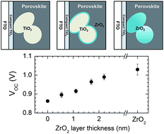
Controlled interfacial electron injection was investigated by surface modification of mesoporous TiO2 film with insulating thin ZrO2 layer in a mesoscopic CH3NH3PbI3 perovskite solar cell. Open-circuit voltage (Voc) was linearly increased with increasing the thickness of the surface ZrO2 film from 863 mV for the bare TiO2 to 988 mV for the surface modified TiO2 with 2.2 nm-thick ZrO2 layer (Voc was 1030 mV for the mesoporous ZrO2), which was due to decrease in electron injection by thickening the surface ZrO2 layer. Change in electron injection was confirmed by photoluminescence spectra. Charge collection was diminished with the surface ZrO2 layer, which might be related to the limited electron diffusion length in the solution-processed perovskite layer due to the reduced injection into TiO2. Fill factor was reproducibly improved by surface modification, which is due to increased shunt resistance. By the controlled electron injection method, a power conversion efficiency was improved from 11.7% to 13.6% by introducing 1.1 nm-thick ZrO2 layer on the TiO2 surface.

1. Introduction

Perovskite solar cells have been proved to be a promising next-generation photovoltaic technology since the report on long-term durable perovskite solar cells in 2012.1 Organometal halide perovskite materials with chemical formula of CH3NH3PbX3 (X = Br or I) were first attempted as sensitizer in dye-sensitized solar cell structure in 2009,2 which showed power conversion efficiency (PCE) of 3–4%. The low PCE in the sensitized structure was improved to 6.5% in 2011 by optimizing coating condition.3 Thanks to the pioneer works on perovskite solar cell, especially on the solid-state perovskite solar cells based on mesoporous TiO2 (ref. 1) and Al2O3 (ref. 4) together with the confirmed long-term stability,1,4 researches on perovskite solar cell has been intensively performed. Consequently, power conversion efficiencies (PCEs) of 18–20% were recently certified.5,6 CH3NH3PbI3 (MAPbI3) material possess intriguing opto-electronic properties such as high absorption coefficient,2,7–9 low reflectivity,9–11 small exciton binding energy,12 photo-induced giant dielectric constant,13 long charge diffusion length ranging from 1 μm for the solution-processed perovskite films14,15 upto 10 μm for the millimeter scale single crystal,16 and high charge carrier mobility.17 Due to the balanced charge transport behavior and small exciton binding energy, MAPbI3 can be applied to various types including mesoscopic structure and p–i–n or p–n junction planar structure.18–21

Electron injection from MAPbI3 to TiO2 is obvious for the sensitization structure, where the MAPbI3 nanodots were deposited locally on TiO2 surface and the mesopores in the TiO2 film were filled with hole transporting spiro-MeOTAD.1 However, working mechanism may be different in case of the mesoscopic structure in which pores of the TiO2 film is filled with MAPbI3. Although charge separation was observed at both TiO2 and spiro-MeOTAD junctions in the mesoscopic structure by transient laser spectroscopy and microwave photoconductivity measurements,22 it was argued that the dominant transport pathway would be the perovskite absorber even in the mesoscopic structure.23 This indicates that electron injection is debatable in the mesoscopic structure with mesoporous TiO2 film impregnated with MAPbI3. We are thus motivated to study on the degree of electron injection in the mesoscopic structure by depositing the electron non-accepting ZrO2 layer24 on TiO2 surface and controlling the thickness of ZrO2 layer.

Here, we report on effect of the ZrO2 layer deposited on TiO2 surface on photovoltaic performance of the mesoscopic structured perovskite solar cell. In order to investigate electron injection behavior, the thickness of the ZrO2 thin layer was varied from about 5 Å to 22 Å by changing the concentration of zirconium butoxide coating solution. Photovoltaic parameters were substantially changed with increasing the ZrO2 layer thickness, where photovoltage increased with ZrO2 layer thickness and eventually approached to that for the pure ZrO2 mesoporous film. Our experimental observation proves that electron injection occurs at least in the interfacial MAPbI3 being in contact with TiO2 surface.

2. Experimental

2.1 Preparation of mesoporous TiO2 films

Anatase TiO2 nanoparticles (average diameter of about 50 nm) were hydrothermally synthesized by two step method.25 The paste was prepared by mixing the TiO2 nanoparticles with terpineol (Aldrich, 99.5%), ethyl cellulose (Aldrich, 46 cp) and lauric acid (Fluka, 96%). The nominal composition of TiO2[thin space (1/6-em)]:[thin space (1/6-em)]terpineol[thin space (1/6-em)]:[thin space (1/6-em)]ethylcellulose[thin space (1/6-em)]:[thin space (1/6-em)]lauric acid was about 1.25[thin space (1/6-em)]:[thin space (1/6-em)]6[thin space (1/6-em)]:[thin space (1/6-em)]0.9[thin space (1/6-em)]:[thin space (1/6-em)]0.1. Fluorine-doped tin oxide (FTO) glass (Pilkington, TEC-8, 8 Ω sq−1) was cleaned by UV/ozone treatment and sonication with ethanol. FTO surface was covered with a thin compact TiO2 layer prior to deposition of the mesoporous TiO2 film by spin-coating the 0.15 M titanium diisopropoxide bis(acetylacetonate) (75 wt%, Aldrich) solution in 1-butanol at stepwise spin rate of 700 rpm for 8 s, 1000 rpm for 10 s, and 2000 rpm for 40 s, which was followed by drying at 125 °C for 5 min and then finally annealed at 500 °C for 15 min. The nanocrystalline TiO2 paste was deposited on the compact TiO2 layer using spin-coating technique at the rate of 2000 rpm for 20 s and subsequently annealed at 550 °C for 1 h in a muffle furnace to obtain mesoporous TiO2 film. Thickness of the annealed mesoporous TiO2 layer was measured to be 300 ± 20 nm by an alpha-step IQ surface profiler (KAL Tencor). The annealed TiO2 film was immersed in the 20 mM TiCl4 (Aldrich) aqueous solution at 70 °C for 10 min. The substrates are washed with distilled water and dried under air flow, which was followed by annealing at 500 °C for 30 min.

2.2 Formation of ZrO2 thin layers on TiO2 surface

A 2-propanol solutions of 0.01 M, 0.02 M, and 0.04 M zirconium(IV) butoxide (Sigma-Aldrich, 80 wt% in 1-butanol) were prepared in argon atmosphere to be used as the precursor solution. 20 μL of the precursor solution was spin-coated on the annealed mesoporous TiO2 film at spin rate of 4000 rpm for 20 s. The film was then dried under N2 flow. After drying at room temperature, the film was annealed at 500 °C for 20 min in air. The thickness was controlled by varying precursor concentration and the number of spin coating/annealing cycles.

2.3 Preparation of mesoporous ZrO2 film

ZrO2 nanoparticles were prepared according to the method reported elsewhere.26 Zirconium(IV) propoxide solution (51.43 mL, 70% in propanol) was mixed with acetic acid (13.5 mL) under argon condition, to which H2O (214.29 mL) was added under vigorous stirring at room temperature. Colorless precipitate was formed. After stirring for about 1 hour, the propanol was removed by evaporation using a rotatory evaporator at 80 °C for 30 min, to which HNO3 (8.57 mL, assay 68–70%) was added and then the solution was aged for about 12 h under stirring at room temperature. A homogeneous and transparent yellowish liquid was observed. The solution was diluted with 19.24 mL of H2O, which was transferred to a Teflon liner autoclave and heated at 230 °C for 12 h. The resultant was washed with EtOH several times. The prepared ZrO2 nanoparticles were mixed with terpineol, ethyl cellulose and lauric acid to make a viscous paste with nominal composition of ZrO2[thin space (1/6-em)]:[thin space (1/6-em)]terpineol[thin space (1/6-em)]:[thin space (1/6-em)]ethyl cellulose[thin space (1/6-em)]:[thin space (1/6-em)]lauric acid = 1[thin space (1/6-em)]:[thin space (1/6-em)]6[thin space (1/6-em)]:[thin space (1/6-em)]0.3[thin space (1/6-em)]:[thin space (1/6-em)]0.1. Mesoporous ZrO2 film was prepared on the compact TiO2 layer by spin coating technique, where 2.5 g of the ZrO2 paste was diluted with 10 mL of EtOH. 0.5 mL of the diluted solution was spin-coated at 2000 rpm for 20 s, which was heated at 550 °C for 1 h. The annealed ZrO2 film was not post-treated with TiCl4. The thickness of ZrO2 film was adjusted to about 300 nm.

2.4 Fabrication of perovskite solar cells

MAPbI3 was deposited by two-step costing method.25 The 20 μL of 1 M solution of PbI2 in N,N-dimethylformamide (DMF, >99% Sigma) was first spin-coated on the mesoporous TiO2 films with and without surface modification and the ZrO2 film at 3000 rpm for 5 s and 6000 rpm for 5 s. The film was dried consecutively at 40 °C for 3 min and 100 °C for 5 min. In the second step, a 200 μL CH3NH3I solution (7 mg of CH3NH3I in 1 mL 2-propanol) was spin-coated onto the dried PbI2 film at 4000 rpm for 30 s and then dried at 100 °C for 5 min to form MAPbI3, where a loading time of 20 s was required prior to spinning. Spiro-MeOTAD hole transporting layer (HTL) was formed on the perovskite capping layer by spin-coating 20 μL of spiro-MeOTAD solution at 4000 rpm for 30 s. The composition of the spiro-MeOTAD solution was composed of 0.06 M spiro-MeOTAD (72.3 mg of spiro-MeOTAD in 1 mL of chlorobenzene), 0.198 M 4-tert-butylpyridine (TBP) and 64 mM Li-TFSI (520 mg Li-TFSI in 1 mL acetonitrile (Sigma-Aldrich, 99.8%)). Au electrode was finally formed on the HTL by thermal evaporation of gold under 1.0 × 10⁻⁵ Torr at 0.7–1.0 Å s−1. The thickness of the deposited Au layer was measured to be about 100 nm.

2.5 Characterizations

Photocurrent (J) and voltage (V) were measured using a solar simulator (Oriel Sol3A class AAA) equipped with 450 W xenon lamp (Newport 6279NS) and a Keithley 2400 source meter. The NREL-calibrated Si solar cell with KG-2 filter was used to adjust light intensity to one sun illumination (100 mW cm−2). While measuring photocurrent and voltage, the cell was covered with a metal aperture mask with area of 0.123 cm2. Incident photon-to-electron conversion efficiency (IPCE) was measured at DC mode using the IPCE system (PV measurement Inc.). A 75 W xenon lamp (USHIO, Japan) was used as a white light source to generate a monochromatic beam. Calibration was conducted using NIST-calibrated photodiode G425 as a standard. The thin layers of ZrO2 deposited on TiO2 surfaces were investigated using a high-resolution transmission electron microscope (HR-TEM, JEOL JEM-2100F) at an acceleration voltage of 200 kV. Steady-state photoluminescence (PL) spectra were collected using a Cary Eclipse Fluorescence Spectrophotometer (Agilent Technologies) with a xenon flash lamp and a photomultiplier tube (PMT) detector. All samples were photoexcited at 530 nm.

3. Results and discussion

Fig. 1 shows HR-TEM images of TiO2 nanoparticles with and without surface modification with thin ZrO2 layers along with that of ZrO2 nanoparticles. Compared to bare TiO2 in Fig. 1(a), deposition of zirconium butoxide solution forms thin layer of ZrO2 on the TiO2 surface. Presence of ZrO2 layer is also confirmed by elemental analysis based on energy dispersive X-ray, which is consistent with previous result.27 Thickness of the surface formed ZrO2 layer increases with increasing the precursor concentration or number of coatings, where ZrO2 layers with average thickness of about 0.5 nm, 1.1 nm, 1.7 nm and 2.2 nm can be coated on the TiO2 surface. Except for the ZrO2 layers formed from single coating of 0.01 M and 0.02 M, conformal coating of ZrO2 layer on TiO2 surface is formed by dual coating. Compared to ∼50 nm in diameter for the TiO2 particle, ZrO2 nanoparticle shows smaller size of around 20 nm in diameter.
image file: c5ra05497d-f1.tif
Fig. 1 High resolution transmission electron microscopy (HR-TEM) images of (a) bare TiO2, surface modified TiO2 by (b) single coating of 0.01 M Zr(OBu)4 (about 0.5 nm), (c) 0.02 M (about 1.1 nm), (d) dual coating of 0.02 M (about 1.7 nm), (e) dual coating of 0.04 M (about 2.2 nm), and (f) bare ZrO2.

Fig. 2(a) and (b) shows SEM images of bare nanocrystalline TiO2 and ZrO2 coated TiO2. In Fig. 2(b), TiO2 nanoparticles coated with ZrO2 shows no significant difference in surface roughness, which indicates that conformal ZrO2 layer might be formed on the surface of TiO2 nanoparticles. Energy dispersive X-ray mapping is further studied to investigate elemental distribution for the ca. 1 nm-thick ZrO2 layer deposited on the TiO2 nanoparticle (Fig. 2(c)). In elemental distribution images, zirconium (Zr) is detected on the edge of the particle, while titanium (Ti) and oxygen (O) are distributed over the whole part of the particle, which confirms that conformal ZrO2 layer is formed on the surface of the TiO2 nanoparticle.


image file: c5ra05497d-f2.tif
Fig. 2 Scanning electron microscopy (SEM) images of (a) mesoporous TiO2 and (b) mesoporous TiO2 coated with ZrO2 (ca. 1 nm). (c) TEM images and energy dispersive X-ray mapping (element distribution images) of the TiO2 nanoparticle coated with ZrO2.

Photovoltaic performance is found to be significantly altered by the surface modification as can be seen in Fig. 3. Short-circuit photocurrent density (Jsc) decreases but open-circuit voltage (Voc) increases predominantly with increasing the thickness of the surface coated ZrO2 layer. Change in Jsc is well consistent with change in IPCE, where IPCE at long wavelength decreases for the 0.5 nm- and 1.1 nm-thick ZrO2 layers. However, decrease in Jsc is observed in the entire wavelength when the ZrO2 layer thickness increases to 1.7 nm and 2.2 nm. Average photovoltaic parameters are listed in Table 1. Voc increases substantially from 0.863 V for bare TiO2 to 0.988 V for 2.2 nm-thick ZrO2 layer on TiO2. In addition, surface modification improves fill factor (FF) by 9.1–11.8%. Increase in both Voc and FF compensate the decreased Jsc, which consequently leads to improvement of PCE. Average PCE is enhanced from 11.7% for the bare TiO2 to 13.6% for the 1.1 nm-thick ZrO2 layer on TiO2, corresponding to 16.2% increment.


image file: c5ra05497d-f3.tif
Fig. 3 (a) Current (I)–voltage (V) curves and (b) incident photon-to-electron conversion efficiency (IPCE) spectra of the MAPbI3 perovskite solar cells depending on concentration of ZrO2 precursor solution for surface modification of mesoporous TiO2 (mp-TiO2). Mesoporous ZrO2 based perovskite solar cell was prepared for comparison. The IV data were collected by scanning from open-circuit to short circuit.
Table 1 Photovoltaic parameters of short-circuit photocurrent density (Jsc), open-circuit voltage (Voc), fill factor (FF) and power conversion efficiency (PCE) of the MAPbI3 perovskite solar cells depending on concentration of ZrO2 precursor solution for surface modification of mesoporous TiO2 (mp-TiO2). The thickness of mesoporous TiO2 layer was 300 ± 20 nm. Mesoporous ZrO2 layer with thickness of about 300 nm was also compared. The data were obtained under AM 1.5G one sun illumination (100 mW cm−2)
Concentration of Zr(OBu)4 Average layer thickness Jsc (mA cm−2) Voc (V) FF PCE (%)
Bare TiO2   21.0 ± 0.18 0.863 ± 0.01 0.646 ± 0.02 11.7 ± 0.49
0.01 M ∼0.5 nm 20.8 ± 0.64 0.896 ± 0.01 0.705 ± 0.02 13.1 ± 0.48
0.02 M ∼1.1 nm 20.6 ± 0.87 0.915 ± 0.01 0.718 ± 0.01 13.6 ± 0.38
Dual 0.02 M ∼1.7 nm 17.2 ± 0.39 0.962 ± 0.01 0.722 ± 0.01 12.0 ± 0.52
Dual 0.04 M ∼2.2 nm 15.9 ± 0.63 0.988 ± 0.01 0.711 ± 0.01 11.2 ± 0.40
Mp-ZrO2   10.9 ± 0.95 1.03 ± 0.03 0.593 ± 0.06 6.74 ± 1.4


In Fig. 4, Jscs calculated based on the IPCE data are compared with Jscs obtained from IV curves. The calculated Jsc from the IPCE data has about 90% of the Jsc obtained from the IV measurement, which indicates that the calculated Jsc is well matched with the observed Jsc with small deviation.


image file: c5ra05497d-f4.tif
Fig. 4 Relationship between photocurrent densities measured by white xenon light (Jsc (IV)) and calculated based on IPCE data.

We plot the photovoltaic parameters as a function of ZrO2 layer thickness in Fig. 5. Jsc is almost invariant with ZrO2 thickness upto ∼1 nm but starts to decrease upon increasing the ZrO2 layer thickness. On the other hand, Voc decreases continuously with ZrO2 thickness. For the case of the mesoporous ZrO2 film, injection from MAPbI3 to ZrO2 will be inhibited because of higher conduction band position and insulating property of ZrO2.28 Thus, free electrons are transported in the perovskite and collected to the photoanode. The highest Voc observed for the mesoporous ZrO2 film is related to Fermi energy level of MAPbI3.28 The large difference in Voc between bare TiO2 film (0.863 V) and bare ZrO2 film (1.03 V) is indicative of evidence of electron injection from MAPbI3 to TiO2. The increasing rate of Voc looks to be extrapolated to Voc for the mesoporous ZrO2 film, which indicates that the amount of electron injection into TiO2 is diminished by increasing the surface ZrO2 layer thickness. The controlled electron injection by the surface ZrO2 layer is also confirmed by PL measurement.


image file: c5ra05497d-f5.tif
Fig. 5 Dependence of Jsc, Voc, FF and PCE on the thickness of ZrO2 layer deposited on TiO2 surface.

Fig. 6 compares PL intensity depending on the surface ZrO2 layer thickness. All the PL peaks are located at around 780 nm, which is well consistent of emission peak of MAPbI3.29 The bare TiO2 film shows lowest PL intensity, while PL intensity increases with increasing surface ZrO2 layer thickness and eventually highest PL intensity is observed from the bare ZrO2 film. When comparing PL intensities of the surface modified TiO2 with those of both bare TiO2 and ZrO2, increase in PL intensity with increasing the surface ZrO2 layer thickness is clearly indicative of reduction of electron injection by the surface coated ZrO2. The tendency of PL intensity correlates with change of Voc with the surface ZrO2 layer.


image file: c5ra05497d-f6.tif
Fig. 6 Photoluminescence (PL) spectra of the FTO/compact-TiO2/mesoporous-TiO2/thin ZrO2 layer/MAPbI3 films and the FTO/compact-TiO2/mesoporous ZrO2/MAPbI3 film.

Fig. 7 shows dark JV curve of devices incorporating bare TiO2 and TiO2 coated with ca. 1.1 nm-thick ZrO2 layer. Shunt and series resistance are obtained from the inverse slope at zero bias and Voc region, respectively.30 Series resistance is increased by 26% (from 6.25 to 7.91 Ω cm−2) with ZrO2 layer, while shunt resistance is increased by 65% (from 23[thin space (1/6-em)]364.49 to 38[thin space (1/6-em)]654.81 Ω cm−2). Therefore, the improved FF is mainly due to the increased shunt resistance. Ideality factor (n) and saturation current (J0) were calculated by fitting the data using following eqn (1),

 
image file: c5ra05497d-t1.tif(1)
where JD, Vb, q, kB, and T represent current density, bias voltage, electron charge, Boltzmann constant, and temperature, respectively. Ideality factor is calculated to be 2.09 for bare TiO2 and 2.32 for ZrO2 coated sample. J0 is estimated to be lowered by ZrO2 coating (2.09 × 10⁻⁷ mA cm−2) compared to bare sample (3.03 × 10⁻⁷ mA cm−2), which correlates with higher Voc by ZrO2 coating.31


image file: c5ra05497d-f7.tif
Fig. 7 Dark current density (J)–voltage (V) curves of MAPbI3 perovskite solar cell incorporating bare TiO2 and TiO2 coated with 1.1 nm-thick ZrO2 layer. Empty circles and solid lines represent the measured data and the fit results, respectively.

IV hysteresis is investigated since planar structure without mesoporous TiO2 film or mesosuperstructured perovskite with scaffold oxide layer such as Al2O3 shows more pronounced IV hysteresis than the mesoscopic structure with mesoporous TiO2 film.32,33 Fig. 8 compares IV hysteresis, where the IV hysteresis of the bare TiO2 is much less than that of the bare ZrO2. Since ZrO2 is non-injection oxide, the structure containing the mesoporous ZrO2 film is similar to those with Al2O3 or without mesoporous oxide layer in terms of electron injection. Thus IV hysteresis of the mesoporous ZrO2 is expected to be severe, which is well consistent with the previous reports showing severs IV hysteresis of planar structure or Al2O3 bearing perovskite.32,33 Such IV hysteresis is thus related to non-injection property in the mesoscopic structure. Compared to IV hysteresis of the bare TiO2 film, more developed IV hysteresis of the surface modified TiO2 with ZrO2 is due to the reduced electron injection into TiO2 by the surface ZrO2 layer. Extent of IV hysteresis provides indirect evidence of interfacial electron injection at TiO2–perovskite junction.


image file: c5ra05497d-f8.tif
Fig. 8 Scan direction dependent IV curves for the perovskite solar cells based on (a) mesoporous TiO2 (without surface modification), (b) surface modified TiO2 with 1.1 nm-thick ZrO2 layer, and (c) mesoporous ZrO2.

Photo-stability of the device with and without ca. 1.1 nm-thick ZrO2 layer is evaluated (Fig. 9). The measurement was conducted under one sun illumination without encapsulation. Both of the devices show severe degradation of PCE during the light soaking in which 90% of initial performance is degraded within an hour. The degradation of PCE looks faster with ZrO2 coating. The poor stability of device with ZrO2 coating is probably related to characteristics of the device similar to planar junction device without mesoporous TiO2 layer (hysteresis, electron transport pathway).34 Our result suggests that stability of perovskite solar cell might be closely related to electron transport pathway.


image file: c5ra05497d-f9.tif
Fig. 9 Evolution of PCE of the devices incorporating bare TiO2 and TiO2 coated with 1.1 nm-thick ZrO2 layer as a function of light soaking time.

4. Conclusion

We investigated interfacial electron injection by means of surface modification of the mesoporous TiO2 film in the mesoscopic perovskite solar cell structure. Voc was found to depend predominantly on thickness of ZrO2 layer. For the non-injection system employing mesoporous ZrO2 film, highest Voc was demonstrated. When assuming that no interfacial injection occurs, Voc is expected to be independent on surface modification. Thus, our experiments evidences obviously that electron injection occurs at TiO2–perovskite interface. By controlling electron injection and thereby optimizing photovoltaic parameters under the given experimental condition, a power conversion efficiency (PCE) was improved by 16.2%, compared to the bare (untreated) TiO2 device.

Acknowledgements

This work was supported by the National Research Foundation of Korea (NRF) grants funded by the Ministry of Science, ICT & Future Planning (MSIP) of Korea under contracts no. NRF-2010-0014992, NRF-2012M1A2A2671721, NRF-2012M3A7B4049986 (Nano Material Technology Development Program) and NRF-2012M3A6A7054861 (Global Frontier R&D Program on Center for Multiscale Energy System).

References

  1. H.-S. Kim, C.-R. Lee, J.-H. Im, K.-B. Lee, T. Moehl, A. Marchioro, S.-J. Moon, R. Humphry-Baker, J.-H. Yum, J. E. Moser, M. Grätzel and N.-G. Park, Sci. Rep., 2012, 2, 591–597 Search PubMed.
  2. A. Kojima, K. Teshima, Y. Shirai and T. Miyasaka, J. Am. Chem. Soc., 2009, 131, 6050–6051 CrossRef CAS PubMed.
  3. J.-H. Im, C.-R. Lee, J.-W. Lee, S.-W. Park and N.-G. Park, Nanoscale, 2011, 3, 4088–4093 RSC.
  4. M. M. Lee, J. Teuscher, T. Miyasaka, T. N. Murakami and H. J. Snaith, Science, 2012, 338, 643–647 CrossRef CAS PubMed.
  5. http://www.nrel.gov/ncpv/images/efficiency_chart.jpg.
  6. N. J. Jeon, J. H. Noh, W. S. Yang, Y. C. Kim, S. Ryu, J. Seo and S. I. Seok, Nature, 2015, 517, 476–480 CrossRef CAS PubMed.
  7. S. D. Wolf, J. Holovsky, S.-J. Moon, P. Löper, B. Niesen, M. Ledinsky, F.-J. Haug, J.-H. Yum and C. Ballif, J. Phys. Chem. Lett., 2014, 5, 1035–1039 CrossRef.
  8. W.-J. Yin, T. Shi and Y. Yan, J. Phys. Chem. C, 2015, 119, 5253–5264 CAS.
  9. Z. Xie, S. Liu, L. Qin, S. Pang, W. Wang, Y. Yan, L. Yao, Z. Chen, S. Wang, H. Du, M. Yu and G. G. Qin, Opt. Mater. Express, 2015, 5, 29–43 CrossRef CAS.
  10. P. Löper, M. Stuckelberger, B. Niesen, J. Werner, M. Filipič, S.-J. Moon, J.-H. Yum, M. Topič, S. D. Wolf and C. Ballif, J. Phys. Chem. Lett., 2015, 6, 66–71 CrossRef.
  11. C.-W. Chen, S.-Y. Hsiao, C.-Y. Chen, H.-W. Kang, Z.-Y. Huang and H.-W. Lin, J. Mater. Chem. A, 2015, 3, 9152–9159 CAS.
  12. Q. Lin, A. Armin, R. C. R. Nagiri, P. L. Burn and P. Meredith, Nat. Photonics, 2015, 9, 106–112 CrossRef CAS PubMed.
  13. E. J. Juarez-Perez, R. S. Sanchez, L. Badia, G. Garcia-Belmonte, Y. S. Kang, I. Mora-Sero and J. Bisquert, J. Phys. Chem. Lett., 2014, 5, 2390–2394 CrossRef CAS.
  14. G. Xing, N. Mathews, S. Sun, S. S. Lim, Y. M. Lam, M. Grätzel, S. Mhaislkar and T. C. Sum, Science, 2013, 342, 344–347 CrossRef CAS PubMed.
  15. S. D. Stranks, G. E. Eperon, G. Grancini, C. Menelaou, M. J. P. Alcocer, T. Leijtens, L. M. Herz, A. Petrozza and H. J. Snaith, Science, 2013, 342, 341–344 CrossRef CAS PubMed.
  16. D. Shi, V. Adinolfi, R. Comin, M. Yuan, E. Alarousu, A. Buin, Y. Chen, S. Hoogland, A. Rothenberger, K. Katsiev, Y. Losovyj, X. Zhang, P. A. Dowben, O. F. Mohammed, E. H. Sargent and O. M. Bakr, Science, 2015, 347, 519–522 CrossRef CAS PubMed.
  17. C. S. Ponseca Jr, T. J. Savenije, M. Abdellah, K. Zheng, A. Yartsev, T. Pascher, T. Harlang, P. Chabera, T. Pullerits, A. Stepanov, J.-P. Wolf and V. Sundstrom, J. Am. Chem. Soc., 2014, 136, 5189–5192 CrossRef PubMed.
  18. N.-G. Park, J. Phys. Chem. Lett., 2013, 4, 2423–2429 CrossRef CAS.
  19. H. J. Snaith, J. Phys. Chem. Lett., 2013, 4, 3623–3630 CrossRef CAS.
  20. H.-S. Kim, S. H. Im and N.-G. Park, J. Phys. Chem. C, 2014, 118, 5615–5625 CAS.
  21. M. Grätzel and N.-G. Park, Nano, 2014, 9, 1440002 CrossRef.
  22. A. Marchioro, J. Teuscher, D. Friedrich, M. Kunst, R. van de Krol, T. Moehl, M. Grätzel and J.-E. Moser, Nat. Photonics, 2014, 8, 250–255 CrossRef CAS PubMed.
  23. V. Gonzalez-Pedro, E. J. Juarez-Perez, W.-S. Arsyad, E. M. Barea, F. Fabregat-Santiago, I. Mora-Sero and J. Bisquert, Nano Lett., 2014, 14, 888–893 CrossRef CAS PubMed.
  24. H.-S. Kim, I. Mora-Sero, V. Gonzalez-Pedro, F. Fabregat-Santiago, E. J. Juarez-Perez, N.-G. Park and J. Bisquert, Nat. Commun., 2013, 4, 2242 Search PubMed.
  25. J.-H. Im, I.-H. Jang, N. Pellet, M. Grätzel and N.-G. Park, Nat. Nanotechnol., 2014, 9, 927–932 CrossRef CAS PubMed.
  26. N. Papageorgiou, M. Grätzel, O. Enger, D. Bonifazi and F. Diederich, J. Phys. Chem. B, 2002, 106, 3813–3822 CrossRef CAS.
  27. H.-W. Kang, J.-W. Lee and N.-G. Park, Faraday Discuss., 2014, 176, 287–299 RSC.
  28. D. Bi, S.-J. Moon, L. Häggman, G. Boschloo, L. Yang, E. M. J. Johansson, M. K. Nazeeruddin, M. Grätzel and A. Hagfeldt, RSC Adv., 2013, 3, 18762–18766 RSC.
  29. C. C. Stoumpos, C. D. Malliakas and M. G. Kanatzidis, Inorg. Chem., 2013, 52, 9019–9038 CrossRef CAS PubMed.
  30. S.-H. Oh, S.-I. Na, J. Jo, B. Lim, D. Vak and D.-Y. Kim, Adv. Funct. Mater., 2010, 20, 1977–1983 CrossRef CAS PubMed.
  31. D. Zhu, J. Xu, A. N. Noemaun, J. K. Kim, E. F. Schubert, M. H. Crawford and D. D. Koleske, Appl. Phys. Lett., 2009, 94, 081113 CrossRef PubMed.
  32. H. J. Snaith, A. Abte, J. M. Ball, G. E. Eperon, T. Leijtens, N. K. Noel, S. D. Stranks, J. T.-W. Wang, K. Wojciechowski and W. Zhang, J. Phys. Chem. Lett., 2014, 5, 1511–1515 CrossRef CAS.
  33. H.-S. Kim and N.-G. Park, J. Phys. Chem. Lett., 2014, 5, 2927–2934 CrossRef CAS.
  34. E. L. Unger, E. T. Hoke, C. D. Bailie, W. H. Nguyen, A. R. Bowring, T. Heumüller, M. G. Christoforo and M. D. McGehee, Energy Environ. Sci., 2014, 7, 3690–3698 CAS.

Footnote

These authors are contributed equally to this work.

This journal is © The Royal Society of Chemistry 2015
Click here to see how this site uses Cookies. View our privacy policy here.