Dopant-configuration controlled carrier scattering in graphene

Benoy Ananda, Mehmet Karakayab, Gyan Prakashc, S. Siva Sankara Saia, Reji Philipd, Paola Ayalaef, Anurag Srivastavag, Ajay K. Soodc, Apparao M. Raob and Ramakrishna Podila*bh
aDepartment of Physics, Sri Sathya Sai Institute of Higher Learning, Puttaparthi, Andhra Pradesh 515134, India
bDepartment of Physics and Astronomy, and Clemson Nanomaterials Center, Clemson University, Clemson, SC 29634, USA. E-mail: rpodila@g.clemson.edu; Tel: +1-864-656-4447
cDepartment of Physics and Center for Ultrafast Laser Applications, Indian Institute of Science, Bangalore, Karnataka 560012, India
dLight and Matter Physics Group, Raman Research Institute, Bangalore, Karnataka 560080, India
eFaculty of Physics, University of Vienna, Strudlhofgasse 4, A-1090 Vienna, Austria
fSchool of Physical Sciences and Nanotechnology, Yachay Tech University, 100119-Urcuquí, Ecuador
gAdvanced Materials Research Group and Computational Nanoscience & Technology Lab, ABV-Indian Institute of Information Technology, Gwalior, Madhya Pradesh 474010, India
hLaboratory of Nano-biophysics, and Center for Optical Materials Science and Engineering Technologies, Clemson University, Clemson, SC 29634, USA

Received 25th March 2015 , Accepted 30th June 2015

First published on 30th June 2015


Abstract

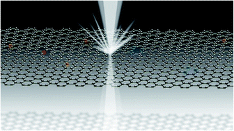
Controlling optical and electronic properties of graphene via substitutional doping is central to many fascinating applications. Doping graphene with boron (B) or nitrogen (N) has led to p- or n-type graphene; however, the electron mobility in doped-graphene is severely compromised due to increased electron-defect scattering. Here, we demonstrate through Raman spectroscopy, nonlinear optical and ultrafast spectroscopy, and density functional theory that the graphitic dopant configuration is stable in graphene and does not significantly alter electron–electron or electron–phonon scattering, that is otherwise present in doped graphene, by preserving the crystal coherence length (La).


Introduction

The discovery of graphene, a two-dimensional atom-thick sheet of sp2 hybridized carbon atoms,1 has led to the experimental realization of quantum mechanical phenomena such as the quantum Hall effect at room temperature,2 quantized optical transmittance,3 non-local hot carrier transport,4 and Klein tunneling.5 More importantly, the distinctive combination of high electron mobility (μ), optical transparency and gate/dopant-tunable carrier density makes graphene an ideal platform for a multitude of photonic and optoelectronic applications over a wide range of frequencies. To truly harness the potential of this combination and make graphene-based efficient optoelectronic devices a reality, energy transport and relaxation pathways of photogenerated carriers in graphene must be tuned appropriately. Defects in graphene are often considered as “performance limiters” since they deteriorate the electron mobility. For example, epitaxial and mechanically exfoliated graphene possess exceptional μ ∼ 15[thin space (1/6-em)]000 cm2 V−1 s−1, whereas their chemical vapor deposition (CVD) grown counterparts exhibit much lower values ∼1–5000 cm2 V−1 s−1 due to the inherent presence of defects.6 Such deterioration in μ primarily arises from the extra electron scattering terms introduced by grain boundaries and defects. Indeed, μ in CVD grown doped graphene is highly compromised compared to that in pristine graphene due to the presence of additional scattering by the substituted dopants and related defects.7 Although there is much effort focused on reducing defects in graphene to improve μ, it should be realized that defects provide an excellent handle and probably the only intrinsic way to control energy transport in graphene. In optoelectronic devices, when photoexcited electrons are scattered by phonons or defects, energy transferred to the lattice is dissipated as heat decreasing the net energy transported through charge carriers to drive a circuit. In the current scenario of graphene optoelectronic devices, a critical challenge is to increase the net charge carrier density and quench electron-defect relaxation pathways to extend photogenerated carrier lifetime. A new energy transport regime in graphene can be realized if electron-defect scattering mechanisms are efficiently quenched.

In this context, it is imperative to identify ideal dopant concentration and configuration in graphene for which the net carrier density (n) can be enhanced (without adversely affecting μ) with quenched electron-dopant scattering mechanisms. Previously, heteroatomic doping was found to result in many changes in the electronic structure of graphene in addition to simply shifting the Fermi level.6 For instance, N-doping in CVD graphene resulted in a bandgap due to the suppression of electronic density of states near the Fermi level and a consequent reduction in μ6–8 It is well known that N atoms can be substitutionally doped in the graphene lattice either in the pyridinic, pyrrolic or graphitic configurations (see Fig. 1(a)).8–16 Our density functional theory (DFT) calculations, described in this article, show that all the three-dopant configurations (pyridinic, pyrrolic, and graphitic) are stable structures with a positive energy (>9.5 eV) released during the formation with graphitic dopants exhibiting the highest stability. In previous studies, we uncovered a strong correlation between the N bonding configuration and the accompanying vibrational properties of N-doped CVD graphene:9 the N atoms bonded in the non-graphitic configurations (pyridinic and pyrrolic, observed using X-ray photoelectron spectroscopy or XPS) resulted in intense Raman D and D′ bands unlike the N atoms bonded in the graphitic configuration, even though the concentration of N dopants was higher in the latter case. Since dopant scattering is one of the dominant factors, which limits the photo-response and electron mobility in doped graphene, it behooves us to investigate the influence of graphitic dopant configuration on the electronic and optical properties of doped graphene for improved device performance. The optical and nonlinear optical (NLO) properties of graphene arise mainly from the inter- and intra-band transitions, and are therefore ideal for probing dopant-induced changes in the electronic band structure of graphene. In tandem with NLO studies, ultrafast pump–probe measurements determine how electron–electron and electron-phonon scattering times (τ2 and τ2 that determine zero-field mobility μ0) vary as a function of crystal coherence length (La) in N-doped graphene. This article juxtaposes data gathered from DFT, Raman, XPS, NLO, and ultrafast spectroscopic studies and concludes that graphitic dopant configuration in N-doped graphene preserves the crystal La, τ1 and τ2 similar to those in pristine graphene. These findings are apt for graphene-based applications such as optoelectronics, mode locking and pulse shaping.12


image file: c5ra05338b-f1.tif
Fig. 1 (a) Different configurations of nitrogen dopants in graphene include graphitic (yellow), pyridinic (orange), and pyrrolic (blue) dopants. (b) Regarding graphene as a two-dimensional electron gas system (2DEG), the average wavelength (λ) of its electrons is determined by the Fermi wavevector (kF) kF = (2πn)1/2, which depends solely on the net carrier density (n). When the crystal coherence length or inter-defect spacing (La) is comparable to λ, carriers scatter off the defects (short relaxation time τ) and the carrier mobility μ is compromised as depicted to the left of the dashed line in the above schematic. Such is the case in doped graphene, where vacancies or dopants present in non-graphitic configurations (e.g., pyrrolic N-dopants shown in purple) significantly reduce La due to their extended interaction volume and thereby scatter electrons (scattering shown by red and maroon colored waves) very effectively. To the contrary, dopants present in graphitic configurations (orange atoms) act as point defects and do not adversely affect τ and μ as shown schematically on the right side of the dashed line.

Materials and methods

N-doped bi-layer graphene synthesis

The N-doped bi-layer graphene used in this study were grown on Cu foils using a previously reported thermal CVD technique.9 Briefly, Cu foils (5 mm × 20 mm) were placed in a 1′′ diameter quartz tube furnace and heated to 1000 °C in 50 sccm of H2 and 450 sccm of Ar flow. Next, 2 sccm of methane was bubbled through a mixture of benzylamine and acetonitrile into the furnace for 30 min, and the samples were cooled to room temperature under flowing H2, Ar, and CH4. The doped bi-layer graphene films formed on Cu foils were then spin-coated with 4% poly-methyl methacrylate (PMMA) in anisole. Subsequently, the Cu foils were etched away using Transene Inc., CE-100 etchant and the bi-layer graphene attached to PMMA was carefully washed in 10% HCl and de-ionized water. Finally, the washed samples were transferred to 0.5 mm thick quartz substrates and annealed at 450 °C in Ar (300 sccm) and H2 (700 sccm) for 2 h to remove the residual PMMA. By varying the volume percent of benzylamine and acetonitrile as 50[thin space (1/6-em)]:[thin space (1/6-em)]50, 0[thin space (1/6-em)]:[thin space (1/6-em)]100, and 75[thin space (1/6-em)]:[thin space (1/6-em)]25 several N-doped graphene samples were prepared with three N concentrations (Fig. 1(a)), which are referred below as S1 (pyrrolic), S2 (graphitic), and S3 (pyridinc), respectively. For each concentration, at least three sister samples were used in our spectroscopic studies.

Open aperture Z-scan

To quantify the absorptive nonlinear characteristics for each of three concentrations S1–S3, open aperture Z-scan technique was employed in both the ns and fs excitation regimes with the excitation source being (a) 5 ns Gaussian pulses of 532 nm from a Q-switched frequency doubled Nd:YAG laser, and (b) 100 fs Gaussian pulses of 800 nm from are generatively amplified mode-locked Ti:Sapphire laser. The incident laser pulses were divided into two by a beam splitter, and the reflected beam was measured by a pyro-electric detector (RjP-735, Laser Probe Inc.) to correct for the pulse-to-pulse energy variations during data acquisition. Using a converging lens, the transmitted beam was focused onto the sample that was mounted on a computer-controlled translational stage. Through repeated knife-edge measurements, the beam radius at the focus was calculated to be ∼20 μm and ∼16 μm for ns and fs excitations, respectively. The beam propagation direction was taken as z with z = 0 being the focus. The input intensity/fluence is different at each z point due to the variation in the cross-sectional area of the focused beam. By translating the sample from −z to +z and measuring the sample transmission at each z point, intensity dependent transmission characteristics of each sample was determined. The measured Z-scan curves, which are plots of sample position vs. transmittance, were analyzed and the coefficients of nonlinearity were obtained from the best-fitted data.

Ultrafast degenerate pump–probe measurements

The ultrafast pump–probe measurements were carried out using 50 fs laser pulses with central photon energy of 1.57 eV derived from a Ti:Sapphire amplifier (Spitfire, Spectra Physics Inc.) operating at a pulse repetition rate of 1 kHz. The spot size (half-width at 1/e maximum) on the sample where the pump and probe beams overlap was kept at ∼600 μm and 400 μm, respectively. The pulse width at the sample as determined using a thin beta-barium borate (BBO) crystal was ∼70 fs. Polarizations of the pump and probe beams were kept perpendicular to each other to prevent scattered pump light from reaching the detector. The pump and probe beams were incident to the sample normal at a small angle of ∼3 degrees between them to maximize their interaction, and their energies were maintained as 12 μJ and 23 nJ, respectively. The pump beam was modulated at 383 Hz using a mechanical chopper and the transmitted probe intensity was measured using a Si-PIN diode with lock-in detection.

DFT modeling

The three types of dopant configurations along with their electron density profiles have been analyzed through density functional theory (DFT) based atomistic tool kit virtual nano lab.17–19 For this computational modeling, the exchange correlation energies have been defined through generalized gradient approximation with revised Perdew–Burke–Ernzerhoff type parameterization, wherein the valence electrons were described by localized pseudo atomic orbital's (PAOs) with double-ζ polarized basis set. A large plane wave mesh cut-off of 150 Ryd is used throughout the calculation with 1 × 10 × 10 k-point sampling to achieve the total energy convergence. In full course of optimization, the run was performed with maximum force tolerance set at 0.05 eV Å−1 and electron temperature 300 K. To verify the structural stability of pristine as well as doped (graphitic, pyridinic and pyrrolic) graphene, the binding energy of the system has been calculated. Formation energy is defined as the energy released on the formation of structure from free atoms and its positive value shows that the sheet is stable after introducing the dopants. It is calculated using the following equation Efor = EddgEdg + nVmCnNmN, where Edg and Eddg are total energies of defected and defected-doped graphene (containing dopants and other defects such as vacancies as in the case of non-graphitic dopants). nV and nN are number of carbon vacancies and nitrogen dopants respectively while mC and mN are the chemical potentials of carbon (in graphene) and nitrogen.

Results and discussion

In a heuristic picture, graphene may be viewed as a two-dimensional electron gas system (2DEG) whose Fermi wave vector (kF) (and hence the wavelength λ of electrons) is determined solely by n as kF = (2πn)1/2. Under this premise, carrier mobility μ or carrier relaxation time τ is impervious to defects when λ is sufficiently large compared to the average defect–defect distance La. Nonetheless, the presence of extended defects at a length scale comparable to λ can compromise μ and τ by efficiently scattering carriers (Fig. 1(b)). The 2DEG picture, though simplistic in nature, is pertinent even for other semi-metals with more intricate Brillouin zones than graphene. Indeed, we have previously demonstrated that the magnitude and temperature dependence of μ and defect scattering in spark plasma sintered pellets of Bi nanoparticles remain unperturbed despite the introduction of defects in the pellet.20 While Bi presents an intriguing example in its own right, CVD-grown bilayer graphene21 serves as an exquisite platform to validate the 2DEG picture, and potentially lead to the realization of doped graphene with excellent μ. Doping graphene without affecting its μ or τ would allow a greater flexibility in the design and optimization of graphene-based nano-photonic, electronic, and optoelectronic devices. Accordingly, we built on the intriguing carbon–nitrogen chemistry to chemically grow bilayer graphene with multiple dopant concentrations and configurations, as described in ref. 9. Here, we go beyond simple synthesis to systematically probe the influence of different dopant concentrations and configurations on the optical, electronic, vibrational properties and carrier dynamics of CVD grown bilayer graphene.

We found that the phonon scattering cross-sections, saturable absorption characteristics and relaxation time constants are strongly influenced by the dopant configuration rather than the dopant concentration. While detailed characterization of our samples is described in ref. 9, a brief overview is presented below for facilitating a comprehensive understanding of the results. The C 1s line in the XPS spectra (Fig. 1 in ref. 9) for pristine and three N-doped graphene samples labeled S1 (pyrrolic), S2 (graphitic), and S3 (pyridinic; see Methods section and Fig. 1(a)) is upshifted (by ∼0.1–0.16 eV) and broadened (by ∼0.5 eV), relative to the pristine sample, with a peak maximum ∼284.61 eV and a full width at half-maximum ∼1 eV. A statistical analysis of N 1s line shape on at least 3 samples confirmed the presence of different configurations for doped N in the graphene lattice: graphitic, pyrrolic and pyridine-like N.22,23 As detailed in ref. 9, we observed that sample S2 exhibits graphitic dopant configuration while S1 and S3 show additional defects such as vacancies and pentagons in the honeycomb lattice appearing due to pyridinic/pyrrolic substitution. Besides identifying the N bonding configurations, we quantified dopant concentration from the relative photoemission cross-sections for the C 1s and the corresponding N 1s (substitutional doping only) peaks in S1, S2 and S3 to be 0.2, 2.5 and 3.8 at% N, respectively.

The Raman spectrum of pristine graphene (Fig. S1) exhibits several sharp features such as the disorder band (D band), graphitic band (G band) and the G′ band. Clearly, the intensity of D band (located at ∼1350 cm−1) relative to the G band (located at ∼1585 cm−1) is low in pristine samples due to their high crystallinity. Interestingly, samples S1 and S3 also exhibited an additional peak at ∼1620 cm−1 (known as the D′ band).24 The origin of the D and D′ band is well understood within the framework of double resonance (DR) where in-plane transverse or longitudinal optical phonon (iTO/iLO) scattering is conserved respectively by inter-valley or intra-valley defect scattering.25 Cancado et al.25 reasoned earlier that the D band is more intense for arm-chair edges (compared to zig–zag edges) since the defect scattering (needed to conserve the iTO scattering) associated with them can connect two inequivalent K and K′ points (or support inter-valley scattering) in the Brillouin zone. In our samples, non-graphitic dopant configuration (samples S1 and S3) generates pores in the graphene sheets, which contain arm-chair like edges and consequently result in the increase in D band intensity relative to the G band intensity. In addition, the D band also broadens more in samples S1 and S3 compared to S2 due to the lattice disruption by dopants bonded in the non-graphitic configuration. It is important to note that the above Raman features were prevalent on a millimeter scale in all our samples.

Our CVD grown samples clearly exhibited a four peaked structure in the G′ band (Fig. S1) with a dispersion ∼85 ± 5 cm−1 eV−1 (data not shown) confirming that the samples are indeed bilayer graphene. The G′ band is also a DR process similar to the D and D′ bands, however, in the DR process for the G′ band two iTO phonons are involved in inter-valley scattering without the need for defects. We previously showed that the G′ band downshifts upon doping graphene with N, as described in ref. 9. Interestingly, we found that the downshift in G′ band is also strongly dependent upon the dopant configuration, i.e., larger downshifts in G′ band were observed for samples S3 (∼25 cm−1) and S1 (10–15 cm−1) which contained N-dopants in non-graphitic configurations relative to sample S2 (1–2 cm−1). It is expected that the presence of edges in the non-graphitic bonding configuration may renormalize the electron and phonon energies more strongly,26 i.e., changes in Fermi and phonon velocities that dictate the dispersion of Raman modes with respect to excitation energy. Such a renormalization leads to a discernible downshift in the G′ band frequency even at low dopant concentrations as seen in sample S1 (cf. Fig. S1).

As discussed next, the above-discussed electronic structure is consistent with our density functional theory calculations. The positive formation energies (>9 eV) for the three-dopant configurations (see Fig. 2) obtained from the DFT modeling confirms their stability (see Methods section). The formation energy of graphitic doping was found to be 10.2 eV, which is higher than 9.9 eV for pristine implying that the graphitic phase is not only the most stable among other dopant configurations but interestingly is also more stable than pristine graphene. While the higher stability of graphitic dopants among doped-graphene phases may be understood in terms of energetically unfavorable vacancies and dangling bonds present in non-graphitic configurations, its stability over the pristine form may be rationalized as follows. In pristine graphene each C atom has three σ bonds with neighboring C atoms and one π bond (sp2 hybridization), whereas in graphitic dopant configuration, the N atom substituting the C atom possess an extra lone pair of electrons after forming 3σ bonds with 3 adjacent C atoms. This extra electron lone pair is in conjugation of double bond of other C atoms around the N atom (i.e., conjugation between N lone pair and σ and π bonds resulting from sp2 hybridization of graphene) and is responsible for the electron resonance, which enhances the stability of graphitic dopants slightly above the pristine form. In addition to the three different configurations discussed in Fig. 2, our DFT calculations showed that the porphyrin-type dopants (see Fig. S2 in ESI) are stable in graphene with a formation energy ∼9.75 eV, which is greater than that of pyrrolic dopants. Although porphyrin-type dopants are more stable than pyrrolic, our detailed XPS studies (discussed in ref. 9) did not detect the presence of this dopant configuration experimentally in samples discussed in this study.


image file: c5ra05338b-f2.tif
Fig. 2 The lattice structure (top 4 panels) of pristine (a), graphitic (b), pyridinic (c), and pyrrolic (d) defects in graphene along with their electron density shown in the bottom panels. The energy released on the formation of structure from free atoms for all the configurations was found to be positive (pristine-9.90 eV, graphitic-10.22 eV, pyridinic-9.77 eV, and pyrrolic-9.55 eV) confirming the stability of N-doped configurations experimentally observed from XPS and Raman spectroscopy.

The Raman spectrum of graphene contains many rich features (e.g., D and G′ bands) that are highly sensitive to inter- and intra-layer defects and interactions. Besides the main D, G, and G′ bands, several other Raman modes such as the combination modes and G* mode ∼2450 cm−1 appear in the spectrum of graphene.27–29 In a Raman process phonons away from the center of the Brillouin zone (Γ point) are often not active since the linear momentum the light is small (∼0.002 nm−1 for 488 nm excitation) when compared with the Brillouin zone dimension (∼13 nm−1 for graphene). However, the K-point phonons are still visible in the Raman spectrum of graphene due to its unique continuous energy levels and phonon dispersion relations which facilitate a high Raman scattering cross-section (Q in eqn (1)) through the DR mechanism.

 
image file: c5ra05338b-t1.tif(1)

In eqn (1), Mxy (x, y = a, b, and c) is the matrix element for the scattering over the intermediate states x and y, El and Elℏω are the energies of the incoming and outgoing photon, Epi (p = a, b, and c) is difference in the energy of electronic level p and the initial level i, and γ is the broadening parameter of the electronic transition between p and i. Previously, May et al.27 and Araujo et al.29 have independently analyzed the G* band and assigned it to a combination mode containing 2 or more peaks arising from iTO and LA phonons scattering electrons to either inner or outer side29 of the Dirac cones at the K/K′-points. As shown in Fig. 3, we clearly observed at least a two-peak structure in the G* band for the pristine samples similar to earlier reports. Interestingly, the G* band vanished completely for samples S1 and S3 while only one peak (as opposed to two peaks in the pristine sample) was found in sample S2 for at least 3 different laser excitations (455, 488, and 514.5 nm). Such an observation may be rationalized as follows. As described in eqn (1), the Raman scattering processes are broadened by the parameter γ that originates from electron–phonon and electron–electron scattering of the photo-excited carriers.30 A fast scattering rate of photo-excited carriers (or low τ) increases γ. The introduction of dopants results in strong electron-defect scattering that reduces the excited carrier-phonon scattering time from ps to hundreds of fs (an order of magnitude decrease) in samples S1 and S3 (evidenced by results described later in Fig. 6) resulting in a high γ or severe broadening of all Raman features. The disappearance of two-peaked structure and the broadening of G* band in sample S2 may also be attributed to a moderate increase in γ. The non-graphitic doping in S1 and S3 induces defects other than N-dopants such as vacancies or edges (see Fig. 1 in ref. 9), which scatter electrons more efficiently than phonons, possibly resulting in the complete disappearance of G* band. Concurring with this scenario, we observed that combination modes (such as iTALO, LOLA, and iTOTA described in ref. 28) are severely broadened in sample S1 and completely disappeared (similar to the G* band) in samples S2 and S3 due to defect-induced scattering and increase in γ (Fig. 4(a)).


image file: c5ra05338b-f3.tif
Fig. 3 (a–c) Raman spectra of CVD grown samples show the presence of two peaks in G* band ∼2450 cm−1 in pristine samples at 3 different Raman excitations. The solid curves below the spectrum are the deconvoluted fits to the experimental data. The G* band broadens in S2 and disappears in S1 and S3 samples due to defect-induced broadening (see text).

image file: c5ra05338b-f4.tif
Fig. 4 (a) The Raman spectra of pristine and N-doped samples showing various combination modes between 1800–2500 cm−1. Clearly, these modes broaden and disappear upon the introduction of dopants due to increase in inhomogenous broadening and electron-defect scattering. The solid curves below each spectrum are the deconvoluted fits. (b) A Fourier transform of time-resolved pump–probe spectrum (discussed later in Fig. 6) showing the low-frequency Raman modes in CVD grown graphene. The broad feature ∼45 cm−1 may be attributed the doubly degenerate (E2g) shear mode shown in (c).

In addition to the linear optical (e.g., π–π* transition) and vibrational properties, we and others previously showed that the nonlinear optical properties of graphene (i.e., saturable absorption) are highly sensitive to the changes in its electronic structure.31,32 Accordingly, we performed open aperture Z-scan studies of S1–S3 to confirm the dopant-induced changes in the electronic structure of host graphene. As shown in Fig. 5(a) and (b), the nonlinear transmittance (both in the ns and fs regimes) increases with input intensity signaling a saturation of absorption in all samples. Numerical simulations based on nonlinear transmission eqn (2) yielded a best fit to the experimental data when a weak two-photon absorption (2PA) component was added to the dominant saturable absorption (SA) within the mathematical model. The pulse propagation equation for such an SA + 2PA type process is given by

 
image file: c5ra05338b-t2.tif(2)
where I is the incident laser intensity, z′ is the propagation distance within the sample, α0 is the linear absorption coefficient, Is is the saturation intensity which characterizes the saturable absorption behavior and β is the 2PA coefficient.31–33 Clearly, the NLO data in Fig. 5 follows a similar trend as observed in the Raman and XPS data underscoring the influence of dopant configuration (over dopant concentration) on the optical properties of N-doped graphene.


image file: c5ra05338b-f5.tif
Fig. 5 Open aperture Z-scan data for pristine graphene, S1, S2 and S3 collected with the (a) ns and (b) fs excitations. The on-axis peak intensity (Io) is 0.16 GW cm−2 and 12.5 TW cm−2, respectively. Solid lines represent theoretical fits to the experimental data obtained from eqn (1) (see text for details). Panels (c) and (d) show the variation of saturation intensity (Is) and the 2PA coefficient (β) obtained from the best fit curves to the Z-scan data in panels (a) and (b). Both Is and β are higher for non-graphitic dopant configuration due to the larger defect density arising from pores and arm-chair like edges (cf. Fig. 2(a)).

image file: c5ra05338b-f6.tif
Fig. 6 (a) Time-resolved differential transmission spectra for pristine graphene and S1–S3 obtained through a degenerate pump–probe method using 70 fs pulses of 780 nm excitation wavelength. Solid lines represent the bi-exponential fits based on carrier–carrier and carrier–phonon scattering time scales (see Table 1). The inset shows the parabolic energy dispersion for bilayer graphene and the arrow indicates excitation of electrons from the valence to the conduction band. (b) Under intense photo-excitation, the non-equilibrium carrier distribution (in the Ek space depicted by the parabolic energy dispersion in the inset shown in (a)) results in an initial rise in the transmitted intensity. The carriers (electron and hole distribution shown in blue and orange respectively) equilibrate by carrier–carrier scattering on a timescale τ1. Subsequently, the carrier thermalization and decay occur through carrier–phonon scattering on a timescale τ2.

The β and Is values31,32,34–38 obtained from the numerical fits for S1 and S3 (non-graphitic configurations) are higher compared to those for S2 (graphitic configuration) and pristine graphene, indicating that NLO properties are also influenced by the renormalization in the electronic energies. A simple increase in n alone cannot rationalize the deduced increase in β or Is values since β and Is of S1 are higher than S2 despite its low N concentration (Fig. 5(c) and (d)). These intriguing, and important, dopant-induced changes in the optical properties of S2 relative to S1 and S3 can be rationalized in terms of the carrier relaxation times through ultrafast degenerate pump–probe (PP) measurements, which we discuss next.

The differential transmittance (ΔT/T) was obtained by taking the ratio of pump-induced change in the probe transmittance (ΔT) at a time t after the pump excitation to the probe transmittance (T) in the absence of a pump (Fig. 6(a)). The initial response is an incident pulse-width-limited rise in the transmitted signal immediately after the zero delay (t = 0), which eventually decays in an exponential manner. The best fit to the PP data was obtained with a bi-exponentially decaying function, ΔT/T = A1[thin space (1/6-em)]exp(−t/τ1) + A2[thin space (1/6-em)]exp(−t/τ2) with two distinct time scales: a fast component (τ1) corresponding to the intraband carrier–carrier scattering and a slower component (τ2) corresponding to carrier–phonon scattering (discussed later in Fig. 6(b)). Both τ1 and τ2 values obtained from the best-fitted curves for the samples are tabulated in Table 1. Consistent with our Z-scan measurements (cf. Fig. 5), the sign of ΔT/T signal in Fig. 6 is positive and is due to the bleaching of ground state (saturable absorption). As shown in Fig. 6(b), under intense photo-excitation a narrow non-equilibrium carrier distribution (akin to a broadened Dirac-delta distribution) is generated in the electron density of states above and below the Fermi level through intra-band and inter-band one-photon absorption (1PA) and 2PA processes.32 Such a non-equilibrium carrier population broadens in momentum via inelastic and elastic intra-band carrier–carrier scattering on a timescale of τ1 (100–200 fs) and equilibrates to reach a Fermi–Dirac distribution with a temperature much higher than the lattice temperature. The hot carriers further cool down by inter-band carrier–phonon scattering on a timescale of τ2 (1–2 ps) and eventually reach a thermal equilibrium with the lattice.32 In the case of carrier trapping, relaxation times are prolonged up to hundreds of ps to a few ns.32 Once a steady state is reached between excited carriers and carriers relaxing back to initial states, further absorption of photons within the pulse width is restricted as two photo-excited carriers cannot occupy the same state due to ‘Pauli blocking’.

Table 1 Carrier relaxation times of both pristine and N-doped graphene obtained from the analysis of time resolved ultrafast pump–probe measurements. Consistent with conclusions drawn from the Raman and NLO data, S2 exhibits similar carrier–carrier (τ1) and carrier–phonon (τ2) relaxation times due to its graphitic N-dopant configuration
Sample ID τ1 τ2
Pristine 241 fs 2 ps
S1 196 fs 206 fs
S2 232 fs 1.6 ps
S3 168 fs 186 fs


As shown in Table 1, the carrier–carrier and carrier–phonon relaxation times do not decrease monotonically with increasing N content, akin to the Raman features described in Fig. 3 and 4 and the saturable absorption intensity in Fig. 5(a) and (b).

Clearly, the dopants present in the non-graphitic configurations exhibit much faster relaxation times relative to dopants present in S2 with graphitic bonding, or pristine graphene. Indeed, carriers in sample S1 decay much faster (within fs), despite lower N content, due to the presence of extended defects that lead to increased contribution from carrier-defect scattering. Since La (nm) = 2.4 × 10⁻¹⁰λ4(IG/ID),25–31 it follows that La (and hence the relaxation time) decreases with an increase in the D band intensity. Clearly, the non-graphitic dopants present in S1 and S3 lower La as they create pores in the honeycomb lattice leading to extended defects (or a high defect-density).

While La, derived from empirical results in nano-crystalline graphite,39 represents the amount of disorder given by one-dimensional defects, Ld or average distance between point defects in single-layer graphene may be obtained as Ld2 (nm) = 1.8 × 10⁻⁹λ4(IG/ID). Since both La and Ld vary inversely with D band intensity (which increases with increasing density of N dopants or defects), carrier relaxation times decrease significantly for S1 and S3 (non-graphitic) compared to S2 and pristine samples. In this context, La is more appropriate than Ld for our samples due to their bilayer character and the nature of extended defects in S1 and S3 (e.g., pores and arm-chair like edge). Considering pristine graphene as a two-dimensional electron gas (2DEG), we can approximate the Fermi wave vector kF ∼ (2πn)1/2 with an average carrier density n ∼ 1012 cm−2. In other words, the carriers in pristine graphene may be considered to have a wavelength ∼25 nm. The IG/ID ratios from the Raman data in Fig. S1 yield La > 100 nm for pristine (106 nm) and S2 (101 nm) samples, which is at least 4 times the carrier wavelength (25 nm). However, S1 and S3 exhibit much shorter La (33 and 25 nm, respectively) which is comparable to the carrier wavelength and consequently support enhanced scattering of carriers (or faster decay times). Considering that μ is directly proportional to τ, it is then expected that μ in the case of S2 is not significantly different from that in pristine graphene, despite the presence of dopants in S2 (since it does not significantly alter La). Such a dopant configuration is advantageous since it increases the carrier concentration and upshifts the Fermi level without compromising the carrier mobility in doped graphene. Returning to saturable absorption behavior of N-doped graphene (cf. Fig. 5), Dawlaty et al. have earlier reported that τ2 in pristine epitaxial graphene decreases concomitantly with La, concurring with our present observation of lower lifetimes for non-graphitic substitution (S1 and S3). The saturation carrier density (Ns) in graphene could be estimated using a simplified approximation given by Bao et al. as Ns = αIτ/ħω where α is the absorption coefficient, ħ is reduced Planck's constant and ω is the excitation frequency.40 Chemla et al. argued that in the case of 2-DEG, absorption saturation occurs when photo-generated carrier density is about one charge carrier per exciton volume 4πa03/3 where a0 is the Bohr radius.41 Therefore saturation intensity can be approximated as Is = 3ħω/4πa03ατ.37 It now follows that for a given excitation, Is is solely determined by τ through an inverse relation. Thus the variation in Is with dopant configuration for both fs and ns excitation regimes shown in Fig. 5(c) and (d) can be explained using the effect of defects on the carrier relaxation times.

Returning to Fig. 4(b), the broadening of Raman features is concurs with the carrier relaxation times derived from the data presented in Fig. 6. In addition to providing the relaxation times, the Fourier transform (FT) of excited carrier decay, shown in Fig. 4(b), contains information pertaining to low-wavenumber phonons. The presence of the Raman excitation line at 0 cm−1 often overwhelms the low-frequency phonon signals in Raman spectroscopy. Recently, Tan et al.42 uncovered a doubly degenerate (Fig. 4(c)) low-wavenumber shear mode (∼45 cm−1) in multilayer graphene using Raman spectroscopy. As shown in Fig. 4(b), we observed a peak in the low-frequency data ∼45 cm−1 in the FT-spectra (derived from Fig. 6(a)), which could plausibly be attributed to the shear mode in our bilayer samples. Not surprisingly, we found that this mode broadened in all the doped samples akin to other features (cf. Fig. 3 and 4) observed directly in the Raman spectrum due to changes in carrier relaxation times. Additional features observed above 45 cm−1 may be Raman inactive acoustic phonons away from the Γ-point and warrant further investigation. Lastly, juxtaposing DFT, Raman, XPS, pump–probe and non-linear optical spectroscopic measurements on N-doped graphene, it could be surmised that both dopant configuration and density play a critical role in determining the properties of graphene. Particularly, an increase in the density of non-graphitic nitrogen dopants is expected to decrease the coherence length La, much more rapidly than graphitic dopants, due to the formation of other accompanying defects such as vacancies or pentagons. This increase in non-graphitic N-dopant density will lead to: (i) a more pronounced decrease in the electronic mobility, compared to graphitic dopants, due to increased defect scattering, (ii) increase the electronic density of states near the Fermi level, and (iii) the appearance of D and D′-bands ∼1350 cm−1 and ∼1620 cm−1.

Conclusions

In summary, we investigated the influence of substitutional N-doping on the electronic, vibrational, and optical properties of CVD grown bi-layer graphene. Our DFT calculations showed that all N-dopant configurations are stable with a positive formation energy. Our XPS measurements indicated that N can be controllably doped in pyridinic, pyrrolic, and graphitic configurations. Interestingly, the D-band intensity increased significantly only when the N-dopants are substituted in non-graphitic configurations since they create pores with armchair edges in the graphene lattice. Furthermore, the Raman G′ band frequency was observed to downshift due to the electron-phonon energy renormalization near dopant sites. The G*, combination, and low-frequency modes (derived from pump–probe data) broadened or disappeared in the Raman spectrum of doped samples due to decreased scattering rates. In the nonlinear regime, the 2PA coefficient and saturation intensity were higher for non-graphitic dopant configuration compared to graphitic configuration, consistent with the Raman scattering data. Most importantly, time-resolved pump–probe spectroscopy studies clearly showed that non-graphitic dopants reduce scattering times of electrons due to a decrease in the crystal coherent length. Lastly, our results imply that N-dopants when substituted in a graphitic configuration yields n-type graphene with little or no deterioration in the electron mobility.

Acknowledgements

Authors from Sri Sathya Sai Institute of Higher Learning (SSSIHL) are grateful to Sri Sathya Sai Baba, the founder chancellor of SSSIHL, for the infrastructure and lab facilities. BA acknowledges senior research fellowship (SRF) from UGC, India. RP and AMR acknowledge the support from US National Science Foundation grant CMMI-1246800 award. RP thanks Prof. Jian He, Department of Physics, Clemson University and Dr Rahul Rao, Honda Research for useful discussions. AS is thankful to ABV-IIITM, Gwalior for the infrastructural support provided for the computational work at CNT Lab.

Notes and references

  1. M. I. Katsnelson, Mater. Today, 2007, 10, 20–27 CrossRef CAS.
  2. K. S. Novoselov, Z. Jiang, Y. Zhang, S. V. Morozov, H. L. Stormer, U. Zeitler, J. C. Maan, G. S. Boebinger, P. Kim and A. K. Geim, Science, 2007, 315, 1379 CrossRef CAS PubMed.
  3. R. R. Nair, P. Blake, A. N. Grigorenko, K. S. Novoselov, T. J. Booth, T. Stauber, N. M. R. Peres and A. K. Geim, Science, 2008, 320, 1308 CrossRef CAS PubMed.
  4. N. M. Gabor, J. C. W. Song, Q. Ma, N. L. Nair, T. Taychatanapat, K. Watanabe, T. Taniguchi, L. S. Levitov and P. Jarillo-Herrero, Science, 2011, 334, 648–652 CrossRef CAS PubMed.
  5. M. I. Katsnelson, K. S. Novoselov and A. K. Geim, Nat. Phys., 2006, 2, 620–625 CrossRef CAS PubMed.
  6. D. Wei, Y. Liu, Y. Wang, H. Zhang, L. Huang and G. Yu, Nano Lett., 2009, 9, 1752–1758 CrossRef CAS PubMed.
  7. H. Wang, T. Maiyalagan and X. Wang, ACS Catal., 2012, 2, 781–794 CrossRef CAS.
  8. A. Lherbier, X. Blase, Y.-M. Niquet, F. Triozon and S. Roche, Phys. Rev. Lett., 2008, 101, 036808 CrossRef.
  9. R. Podila, J. Chac, J. T. Spear, T. Pichler, P. Ayala and A. M. Rao, Appl. Phys. Lett., 2012, 123108, 3–6 Search PubMed.
  10. L. Feng, Y. Chen and L. Chen, ACS Nano, 2011, 5, 9611–9618 CrossRef CAS PubMed.
  11. H. M. Jeong, J. W. Lee, W. H. Shin, Y. J. Choi, H. J. Shin, J. K. Kang and J. W. Choi, Nano Lett., 2011, 11, 2472–2477 CrossRef CAS PubMed.
  12. Z. Jin, J. Yao, C. Kittrell and J. M. Tour, ACS Nano, 2011, 5, 4112–4117 CrossRef CAS PubMed.
  13. B. Guo, Q. Liu, E. Chen, H. Zhu, L. Fang and J. R. Gong, Nano Lett., 2010, 10, 4975–4980 CrossRef CAS PubMed.
  14. D. Usachov, O. Vilkov, A. Grüneis, D. Haberer, A. Fedorov, V. K. Adamchuk, A. B. Preobrajenski, P. Dudin, A. Barinov, M. Oehzelt, C. Laubschat and D. V. Vyalikh, Nano Lett., 2011, 11, 5401–5407 CrossRef CAS PubMed.
  15. X. Wang, X. Li, L. Zhang, Y. Yoon, P. K. Weber, H. Wang, J. Guo and H. Dai, Science, 2009, 324, 768–771 CrossRef CAS PubMed.
  16. L. Zhao, R. He, K. T. Rim, T. Schiros, K. S. Kim, H. Zhou, C. Gutiérrez, S. P. Chockalingam, C. J. Arguello, L. Pálová, D. Nordlund, M. S. Hybertsen, D. R. Reichman, T. F. Heinz, P. Kim, A. Pinczuk, G. W. Flynn and A. N. Pasupathy, Science, 2011, 333, 999–1003 CrossRef CAS PubMed.
  17. Atomistix ToolKit version 13.8, QuantumWise A/S, http://www.quantumwise.com Search PubMed.
  18. M. Brandbyge, J.-L. Mozos, P. Ordejón, J. Taylor and K. Stokbro, Phys. Rev. B: Condens. Matter Mater. Phys., 2002, 65, 165401 CrossRef.
  19. J. M. Soler, E. Artacho, J. D. Gale, A. García, J. Junquera, P. Ordejón and D. Sánchez-Portal, J. Phys.: Condens. Matter, 2002, 14, 2745 CrossRef CAS.
  20. P. Puneet, R. Podila, S. Zhu, M. J. Skove, T. M. Tritt, J. He and A. M. Rao, Adv. Mater., 2013, 25, 1033–1037 CrossRef CAS PubMed.
  21. Y. Zhang, T.-T. Tang, C. Girit, Z. Hao, M. C. Martin, A. Zettl, M. F. Crommie, Y. R. Shen and F. Wang, Nature, 2009, 459, 820–823 CrossRef CAS PubMed.
  22. P. Ayala, A. Grüneis, T. Gemming, D. Grimm, C. Kramberger, M. H. Rümmeli, F. L. Freire, H. Kuzmany, R. Pfeiffer, A. Barreiro, B. Büchner and T. Pichler, J. Phys. Chem. C, 2007, 111, 2879–2884 CAS.
  23. A. L. Elías, P. Ayala, A. Zamudio, M. Grobosch, E. Cruz-Silva, J. M. Romo-Herrera, J. Campos-Delgado, H. Terrones, T. Pichler and M. Terrones, J. Nanosci. Nanotechnol., 2010, 10, 3959–3964 CrossRef PubMed.
  24. G. Keskar, R. Rao, J. Luo, J. Hudson, J. Chen and A. M. Rao, Chem. Phys. Lett., 2005, 412, 269–273 CrossRef CAS PubMed.
  25. L. G. Cancado, M. Pimenta, B. Neves, M. Dantas and A. Jorio, Phys. Rev. Lett., 2004, 93, 247401 CrossRef CAS.
  26. I. O. Maciel, N. Anderson, M. A. Pimenta, A. Hartschuh, H. Qian, M. Terrones, H. Terrones, J. Campos-Delgado, A. M. Rao, L. Novotny and A. Jorio, Nat. Mater., 2008, 7, 878–883 CrossRef CAS PubMed.
  27. P. May, M. Lazzeri, P. Venezuela, F. Herziger, G. Callsen, J. Reparaz, A. Hoffmann, F. Mauri and J. Maultzsch, Phys. Rev. B: Condens. Matter Mater. Phys., 2013, 87, 075402 CrossRef.
  28. R. Rao, R. Podila, R. Tsuchikawa, J. Katoch, D. Tishler, A. M. Rao and M. Ishigami, ACS Nano, 2011, 5, 1594–1599 CrossRef CAS PubMed.
  29. P. T. Araujo, D. L. Mafra, K. Sato, R. Saito, J. Kong and M. S. Dresselhaus, Phys. Rev. Lett., 2012, 109, 046801 CrossRef CAS.
  30. Z. Luo, C. Cong, J. Zhang, Q. Xiong and T. Yu, Carbon, 2012, 50, 4252–4258 CrossRef CAS PubMed.
  31. R. Podila, B. Anand, J. T. Spear, P. Puneet, R. Philip, S. S. S. Sai and A. M. Rao, Nanoscale, 2012, 4, 1770–1775 RSC.
  32. J. M. Dawlaty, S. Shivaraman, M. Chandrashekhar, F. Rana and M. G. Spencer, Appl. Phys. Lett., 2008, 92, 042116 CrossRef PubMed.
  33. R. L. Sutherland, Handbook of Nonlinear Optics, Marcel Dekker Inc., New York, 1996 Search PubMed.
  34. B. Anand, A. Kaniyoor, S. S. S. Sai, R. Philip and S. Ramaprabhu, J. Mater. Chem. C, 2013, 1, 2773 RSC.
  35. H. Yang, X. Feng, Q. Wang, H. Huang, W. Chen, A. T. S. Wee and W. Ji, Nano Lett., 2011, 11, 2622–2627 CrossRef CAS PubMed.
  36. S. Kumar, M. Anija, N. Kamaraju, K. S. Vasu, K. S. Subrahmanyam, A. K. Sood and C. N. R. Rao, Appl. Phys. Lett., 2009, 95, 191911 CrossRef PubMed.
  37. S. Kaniyankandy, S. N. Achary, S. Rawalekar and H. N. Ghosh, J. Phys. Chem. C, 2011, 115, 19110–19116 CAS.
  38. G.-K. Lim, Z.-L. Chen, J. Clark, R. G. S. Goh, W.-H. Ng, H.-W. Tan, R. H. Friend, P. K. H. Ho and L.-L. Chua, Nat. Photonics, 2011, 5, 554–560 CrossRef CAS PubMed.
  39. L. G. Cancado, A. Jorio, E. H. M. Ferreira, F. Stavale, C. A. Achete, R. B. Capaz, M. V. O. Moutinho, A. Lombardo, T. S. Kulmala and A. C. Ferrari, Nano Lett., 2011, 11, 3190–3196 CrossRef CAS PubMed.
  40. Q. Bao, H. Zhang, Y. Wang, Z. Ni, Y. Yan, Z. X. Shen, K. P. Loh and D. Y. Tang, Adv. Funct. Mater., 2009, 19, 3077–3083 CrossRef CAS PubMed.
  41. D. S. Chemla and D. A. B. Miller, J. Opt. Soc. Am. B, 1985, 2, 1155 CrossRef CAS.
  42. P. H. Tan, W. P. Han, W. J. Zhao, Z. H. Wu, K. Chang, H. Wang, Y. F. Wang, N. Bonini, N. Marzari, N. Pugno, G. Savini, A. Lombardo and A. C. Ferrari, Nat. Mater., 2012, 11, 294–300 CrossRef CAS PubMed.

Footnote

Electronic supplementary information (ESI) available: ESI contain Raman spectroscopic measurements of the pristine and N-doped graphene samples. See DOI: 10.1039/c5ra05338b

This journal is © The Royal Society of Chemistry 2015
Click here to see how this site uses Cookies. View our privacy policy here.