DOI:
10.1039/C5RA05257B
(Paper)
RSC Adv., 2015,
5, 46640-46647
Prediction of half-semiconductor antiferromagnets with vanishing net magnetization†
Received
24th March 2015
, Accepted 27th April 2015
First published on 27th April 2015
Abstract
Half-metallic antiferromagnets have proven to be promising candidates for spintronic applications, since the zero net magnetization leads to low stray fields. Here, using a self-consistent DFT + U approach, we found that in a two-dimensional semiconductor codoped with different transition metal pairs, spin-polarized electrons and zero magnetization co-exist. We systematically investigated a Fe–Cr codoped monolayer boron nitride (BN) sheet. Interestingly, the Fe–Cr codoping in the BN sheet induces a half-semiconductor feature, with fully spin-polarized valence and conduction bands belonging to the same spin channel and completely compensated spontaneous magnetization. We propose that this type of materials are half-semiconductor antiferromagnets (HSCAF). Spin gapless semiconductor antiferromagnets (SGSAF) with zero net magnetism are also achieved in such codoped systems. Moreover, we find that HSCAF can be realized in other two-dimensional materials, such as monolayer AlN and GaN with Cr–Ni and Mn–Co codoping, respectively. The HSCAF and SGSAF not only represent promising candidates for spintronics, but also enrich the concept of magnetic materials.
1 Introduction
Manipulation of spin degrees of freedom in electronic devices is the main task of spintronics for promising next-generation electronics technology.1 Lots of efforts have been devoted to designing new materials or structures to manipulate spin-polarized current. Half-metals (HM),2 behaving as metallic in one spin channel but as an insulator or a semiconductor in the opposite spin channel as shown in Fig. 1(a), show potential for spintronics as spin filters, detectors and sensors, and have a theoretically infinite magnetoresistance.3 Half-semiconductors (HSC),4,5 showing semiconductor characteristics with full spin polarization in the same spin channel at the valence band maximum (VBM) and the conduction band minimum (CBM), as shown in Fig. 1(b), are new candidates for the generation and manipulation of spin currents for spintronics. Previous studies indicated that HSC show promising application in negative magnetoresistance6 and spin injection/detection.5 Spin gapless semiconductors (SGS),7 with fully spin-polarized electrons and holes as shown in Fig. 1(c), were firstly proposed by Wang.7 Some remarkable phenomena have been observed experimentally in SGS including colossal electroresistance, giant magnetoresistance8 and crossover of magnetoresistance.9 Most intriguingly, Mn2CoAl with a spin gapless semiconducting nature has been synthesized in experimental work, exhibiting a Curie temperature of 720 K and nearly temperature-independent conductivity and carrier concentration.10 Moreover, HSC and SGS, similarly to HM, show quantized net magnetism per unit cell due to the existence of the gap for their majority and minority channels.
 |
| | Fig. 1 Electronic structure diagrams for (a) half-metals (HM), (b) half-semiconductors (HSC) and (c) spin gapless semiconductors (SGS). | |
In general, HM, HSC and SGS show spin polarization and behave as ferromagnets. However, van Leuken and de Groot11,12 proposed that half-metallic antiferromagnets (HMAF) can be achieved in nonmagnetic materials with a completely spin-polarized current. This magnetic behaviour, with half-metallic characteristics but without any net magnetization, has been theoretically predicted in V7MnFe8Sb7In alloys,11 perovskite oxides,13,14 the Mott insulator NiO,15 a monolayer superlattice16 and in diluted magnetic semiconductors.17 HMAF have potential applications in novel spin-polarized STM tips,12 in new spin injection devices and in single spin superconductivity13 due to their unique properties. Thus far, the most interesting issue is whether antiferromagnetic (fully compensated magnetic moment) HSC and SGS without any net magnetization can be achieved. Such materials might possess significant potential in spintronics due to their semiconducting characteristics. Ferromagnetic HM, HSC and SGS will form magnetic domains and a stray field, which unavoidably restricts the generation of a spin-polarized current. Such a drawback can be overcome if ferromagnetic HM, HSC and SGS are replaced with nonmagnetic spin-polarized HM, HSC and SGS. These classes of materials are named as half-semiconductor antiferromagnets (HSCAF) and spin gapless semiconductor antiferromagnets (SGSAF). The concept of SGSAF has been proposed in the report of Wang;7 however, it has not been achieved in real materials yet.
Moreover, two-dimensional (2D) monolayer materials, such as graphene,18,19 have shown unique properties and tremendous possible applications in nanoscale devices. Transition metal (TM) impurities profoundly influence the electronic and magnetic properties of graphene.20–25 However, the zero band gap of graphene leads to the TM d states strongly coupling with the conduction or valence bands of graphene. It is difficult to obtain the electronic structures of HSC and HM by TM doping. Recently, some wide gap semiconductor materials, such as monolayer BN, AlN, GaN and ZnO, have been theoretically predicted26,27 and synthesized in experiments,28,29 and are promising materials for spintronics. When wide band gap semiconductors are TM-doped, the electronic structures of the systems are primarily determined by the distribution of TM d states around the Fermi level, because the energies of TM 3d orbitals can exist inside the band gap, by which novel magnetic order can be achieved; for example, TM-doped BN sheets have shown HSC, HM and SGS magnetic characteristics.30–32 Here, we take a BN sheet as a typical template to explore the possibility of achieving HSCAF and SGSAF with a TM codoping technique. We find that, in order to use the TM codoping technique to obtain HSCAF and SGSAF, two conditions must be fulfilled: (i) the two TMs must have the same spin states, and (ii) the coupling between the TMs and the host semiconductor must maintain robust antiferromagnetic order (spin singlet) of the TMs. Previous works31,33 have indicated that when single Fe and Cr are doped in the B–N divacancy (DV) of a BN sheet (here the BN sheet with a DV is named as BN-DV for short), the BN-DV is not only extremely stable but also exhibits the same high-spin state, with 4μB magnetic moments. This suggests that if Fe and Cr formed a ‘nonmagnetic FeCr spin singlet dimer’ with completely compensated antiferromagnetic coupling, the combination of defects and TM atoms might be a possible candidate for HSCAF or SGSAF. In the present work, we find a viable approach to achieve HSCAF and SGSAF, through the codoping of a boron nitride (BN) sheet with Fe and Cr pairs. Such a fully spin-polarized material with a compensated zero magnetic moment not only provides two promising candidates for spintronics, but also enriches the concept of magnetic materials.
 |
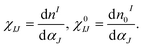
| | Fig. 2 The interacting (χ) and Kohn–Sham response (χ0) functions of single Fe and Cr doped on the BN-DV system. | |
2 Models and computational methods
Our calculations have been implemented in density functional theory (DFT) using the Vienna ab initio simulation package (VASP) code,34,35 with projector augmented wave (PAW) potentials36 to describe the electron-ionic core interaction. A supercell containing 110 atoms is adopted for the calculation model, where a vacuum space of 15 Å perpendicular to the BN plane is chosen. A plane-wave kinetic energy cutoff of 500 eV is employed. The Brillouin zone (BZ) is sampled using 5 × 5 × 1 and 9 × 9 × 1 gamma-centered Monkhorst–Pack grids for the calculations of relaxation and electronic structures, respectively. The criteria of energy and atom force convergence are set to 10−5 eV per unit cell and 0.015 eV Å−1, respectively.
Previous studies25,37,38 indicated that, for TMs on two-dimensional materials like graphene, BN sheets, graphyne and graphdiyne etc., the magnetic states are sensitive to Hubbard U correction. Therefore, to account for the correlation energy of the strongly localized 3d orbitals of the TM atoms, a Hubbard U correction is employed (DFT + U method). In general, the magnitude of the U parameter can be evaluated from experimental data. The linear response theory (LRT) introduced by Cococcioni et al.39 has been successfully applied in TM atom- and dimer-doped two-dimensional systems,37,38,40,41 molecular magnets42 and in a magnetic cluster.43 In the present work, the effective on-site Coulomb repulsion parameter, U, of the single TM-doped BN-DV system (as shown in Fig. S1†) is calculated by the LRT method. The U parameter can be calculated directly by a response function as follows:
| |
 | (1) |
In the linear-response approach, χIJ and χ0IJ are obtained from the response of d state occupations to a small localized perturbation potential, αI, and then the parameter U can be obtained from the following formula:
| |
 | (2) |
By changing the rigid potential shifts, α, we obtain the bare and self-consistent occupation regression response functions. The interacting (χ−1) and the Kohn–Sham (χ0−1) inverse matrices are the slopes of the bare and self-consistent regression response functions, respectively, as shown in Fig. 2. The calculated effective U values for Fe and Cr are 3.15 eV and 2.18 eV, as shown in Fig. 2. In our present work, the separation distances of the Fe–Cr dimer are all larger than 4.24 Å. Such distances suggest that there are no direct interactions or bonding between the Fe–Cr atoms. Moreover, the d orbitals of the TM atoms on the surface of the BN-DV are localized. We can see the localized characteristics of the d orbitals by the spin polarized density as shown in Fig. 3(c) and (d). Wu et al.40 and Lisenkov et al.44 have reported that, in the study of TM atom-doped graphene systems based on GGA + U, the Hubbard U of the TM dimer can safely be approximated by the Hubbard U of a single TM atom, due to the location of the TM dopant on the graphene. Based on the above, we apply U = 2.18 and U = 3.15 eV (from the single TM-DV system) to all the TM dimer calculations. We also compare the influence of the deviation of U in U = 2 eV and U = 4 eV with respect to the linear response U value (UFe = 3.15 and UCr = 2.81). The deviation of U does not affect the qualitative conclusion, the doped system still maintain the semiconductor feature and AF coupling, which will be further discussed below.
 |
| | Fig. 3 The d orbitals of codoped Cr2+ and Fe2+ ions under (a) FM and (b) AF coupling. The blue and green arrows indicate spin up and spin down electrons, respectively, and the red arrows without and with a green cross indicated that hopping is permitted or forbidden, respectively. Panels (c) and (d) show the spin-polarized charge density (SCD) distributions for configuration d (the most stable codoping configuration, see Fig. 4) under FM and AF coupling, respectively. The dark (red) and light (green) isosurfaces denote the spin-up and spin-down charge density, respectively. The isosurface of the SCD is 0.005 e Å−3. | |
3 Results and discussion
3.1 Stability and spin-states of single Fe/Cr and Fe–Cr dimer
Huang et al.33 proposed that, because the energies of TM 3d orbitals are roughly located within the wide energy gap of BN, the TM behaves as a TM2+ ion after interacting with the in-gap defect states of the double-acceptor DV. Here, we firstly performed DFT + U calculations to study single Cr/Fe-doped BN-DV. The results indicate that both single Fe- and Cr-doped systems show high-spin states with a magnetic moment of 4μB per unit cell; similar high-spin states have been reported in Fe- and Cr-doped graphene, BN, ZnO and g-C3N4.25,31,33,38,45,46 Cantalupo et al. reported that a HS state of Fe ions is something which is very peculiar in planar molecular magnets.47 To verify whether the correct spin states were obtained, we calculated the dependence of the energy difference between the HS and LS configurations (defined as ΔELH = ELS − EHS), and the electronic structure, on the Hubbard U term. This approach has been successfully applied to an iron heme complexes system.42 As shown in Fig. S1,† as the U parameter increases, it is found that this can lead to the increasing exchange splitting of spin-up and spin-down. For a transition metal-doped BN sheet, the spin states originate from the competition between crystal field splitting and exchange splitting.33 At all calculated U value, a high spin states is preferred, which is similar to TM in other systems. Some works reported that the HS state of Fe is special for a planar geometry in a molecular magnet.47 However, for Fe-doped BN-DV, the result shows high-spin ground states. From the calculated ΔELH, it is found that an increasing Hubbard U will promote the stability of high-spin states. Moreover, the Hubbard U correction also reduces the binding energy of the TM-BN sheet. For example, the binding energy of Fe–BN is reduced from 7.52 to 5.68 eV with an increasing Hubbard U correction from 0 to 5 eV. The results also indicate that although the Hubbard U correction tends to reduce the binding energy, the binding energies still show high stability (5.68 eV). The Hubbard U correction also influences the equilibrium bond lengths between a TM atom and BN (denoted dTM−B and dTM−N) as shown in Fig. S1.† Therefore, it is crucial to accurately account for the electron correlation of the TM-doped BN-DV sheet. Here, we used the linear-response method to evaluate the Hubbard U parameter and describe the TM-BN system. Our results indicate that the Cr and Fe show stable high-spin states, behaving as Cr2+ and Fe2+ ions in the DV of BN with d4↑d0↓ and d5↑d1↓ spin configurations, respectively. This conclusion is the same as those in previous reports of other groups.31,33
We next used a Cr- and Fe-codoped BN sheet, where each of them fills a BN-DV separately. Because the TM-doped BN system shows extremely high stability, the TMs prefer to dispersedly absorb in the defects of the BN. We briefly compare the energy between an indirect and a direct interaction of a Cr–Fe dimer; the energy of an indirect Cr–Fe dimer is (about 4.05 eV) more stable than that of the direct configuration, which is against the cluster effect, as shown in Fig. S2.† Therefore, we only consider non-merged DV cases, in which the Fe and Cr atoms maintain an indirect interaction without direct Fe–Cr bonds. All possible configurations are considered and schematically summarized in Fig. 4. Table 1 shows the relative energy with respect to the most stable configuration, d, as shown in Fig. 4 (i.e. Fe and Cr atoms doped into two next nearest neighbor (NN) non-merging DVs of BN with a separation of 4.24 Å). The relative stability sequence of the typical Fe–Cr codoped BN-DV systems is d > b > f > c > h > e > a > g > i. In general, the relative energy is dependent on the distance between the two TMs in non-merged DV cases. For instance, the configurations e, g and h show higher relative energies, with larger distances between the TMs.
 |
| | Fig. 4 Schematic of the typical Fe and Cr codoping configurations on the B–N divacancy of BN. Even though each supercell has 110 atoms, only the relevant portions of the supercells are shown in the figure for clarity. | |
Table 1 The calculated results of the Fe- and Cr-codoped BN-DV system under nine typical configurations. The term ‘M.O.’ represents the magnetic order between the Fe and Cr atom. The ΔE represents the relative energy for different Fe- and Cr-codoped configurations. Eex is the energy difference, defined as Eex = EFM − EAFM, where EFM and EAFM are the total energies of the Fe- and Cr-codoped BN-DV system under ferromagnetic and antiferromagnetic states, respectively. The MCr, MFe, MAF, and MFM are the local magnetic moments of the TM atoms and the total magnetic moments under FM and AF states per unit cell. The term ‘ES’ denotes the electronic structure of the codoped system. Egap defines the difference between the HOMO and the LUMO, i.e. Egap = EHOMO − ELUMO. D is the distance between Fe and Cr for different configurations
| Con. |
M.O. |
ΔE (eV) |
Eex (meV) |
MCr (μB) |
MFe (μB) |
MAF (μB) |
MFM (μB) |
ES |
Egap (eV) |
D (Å) |
| a |
AF |
0.738 |
11 |
3.686 |
−3.466 |
0 |
8 |
HSCAF |
0.38 |
5.12 |
| b |
AF |
0.407 |
18 |
3.724 |
−3.503 |
0 |
8 |
HSCAF |
1.06 |
4.30 |
| c |
AF |
0.674 |
107 |
3.583 |
−3.375 |
0 |
8 |
HSCAF |
0.65 |
4.29 |
| d |
AF |
0 |
32 |
3.362 |
−3.179 |
0 |
8 |
SGSAF |
0 |
4.24 |
| e |
AF |
0.681 |
1.3 |
3.692 |
−3.482 |
0 |
8 |
HSCAF |
0.32 |
6.67 |
| f |
AF |
0.512 |
67 |
3.647 |
−3.403 |
0 |
8 |
HSCAF |
0.36 |
4.84 |
| g |
AF |
0.783 |
0.7 |
3.686 |
−3.459 |
0 |
8 |
HSCAF |
0.68 |
8.31 |
| h |
AF |
0.677 |
3.6 |
3.677 |
−3.474 |
0 |
8 |
HSCAF |
0.66 |
6.00 |
| i |
AF |
0.849 |
3.1 |
3.661 |
−3.460 |
0 |
8 |
HSCAF |
0.58 |
5.88 |
3.2 Magnetic and electronic properties
For all the Fe–Cr codoped BN-DV systems, the magnetic moments are 8μB and 0μB when the system is under FM and AFM coupling states, respectively. The results of the local magnetic moments indicate that both Fe and Cr are in the HS state, with d5↑d1↓ and d4↑d0↓ spin configurations, respectively; they behave as a Fe2+ and Cr2+ ion pair in the BN-DV system. This is similar to the case of the single Fe-/Cr-doped BN-DV systems. Table 1 lists the energy differences (Eex = EFM − EAF) between the FM and AFM states for all codoped configurations, as well as the spin magnetic moments of the Fe2+ and Cr2+ ions. A number of very interesting properties can be observed in Table 1, the most intriguing one being the formation of a ‘nonmagnetic FeCr singlet dimer’ under the AFM state with a zero net magnetic moment per cell for all configurations. Regardless of the orientation and the distance between the Fe2+ and Cr2+ ions, the results demonstrate considerable Eex values. The Eex values depend on the distance, the orientation of the Fe–Cr dimer and the mediation of B/N atoms. According to previous reports, a Co dimer being embedded in the DV of graphene nanoribbons (GNRs) leads to a magnetic anisotropy of FM and AFM coupling, because of the spin polarization induced by both the Co and the ribbon edge.44 Unlike the different magnetic coupling of the Co dimer in the DV of GNRs,44 each Fe–Cr-codoped BN-DV configuration shows antiferromagnetic coupling. Moreover, Fe and Cr also induce the magnetic moments of their neighboring B and N atoms, but the total magnetic moment of the systems is zero, indicating completely compensated antiferromagnetism. The above results indicate that the Fe–Cr-codoped BN-DV system can achieve completely compensated antiferromagnetism.
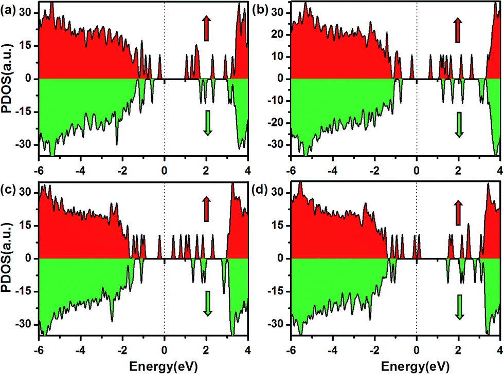
The calculated density of states (DOS) for several of the Fe–Cr-codoped BN-DV systems, shown in Fig. 5, indicate that 100% spin polarization is shown in the HOMO and LUMO with the same majority spin channel. Therefore, the Fe–Cr-codoped BN-DV systems achieve the magnetic order of HSCAF. For example, the DOS of configurations b, c and a, as shown in Fig. 5(a)–(c), demonstrate that both the majority and minority spin channels are semiconducting, and the HOMO and LUMO states belong to the same majority spin channel with an energy gap (the difference between the HOMO and LUMO states, Egap = EHOMO − ELUMO) of 1.06, 0.65 and 0.36 eV, respectively. The three typical systems behave as HSCAF. However, for configuration d, shown in Fig. 5(d), the HOMO and LUMO (majority spin channel) touch each other at the Fermi level, whereas the minority spin channel shows an insulator gap. The results of the energy band structures indicate that the majority spin channel has a small gap of about 0.09 eV. According to the definition of SGS by Wang,7 the term “gapless” is used for an narrow energy gap that is approximately smaller than 0.1 eV. Therefore, the most stable configuration, d, realizes spin gapless semiconducting antiferromagnetic behaviour. For the other configurations, our results indicate that similar electronic structures with half-semiconducting antiferromagnetic behaviour can be obtained, as listed in Table 1. Overall, our results reveal that HSCAF and SGSAF can be achieved via Fe–Cr-codoped BN-DV systems.
 |
| | Fig. 5 The total density of states (DOS) of typical configurations b (a), c (b), a (c) and d (d). The red and blue represent the majority and minority spin channels, respectively. The Fermi level is set to zero. | |
3.3 Mechanism of coexistence of zero magnetism and spin polarization
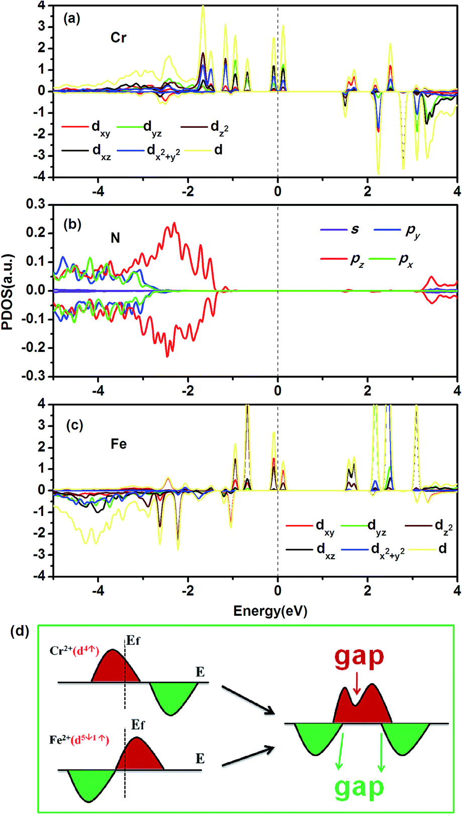
To explain the exotic electronic structures of the Fe–Cr-codoped BN-DV systems, it is necessary to thoroughly study the bonding mechanism along with the AFM coupling between Cr2+ and Fe2+. We take the most stable configuration, d, as an example to illustrate the origin of AF coupling, due to the similar characteristics of the electronic structures of the other codoped systems. From the PDOS of configuration d, as shown in Fig. 6, the majority d states of the Cr atom mainly lie below the Fermi level within the [−2.1 eV, 0 eV] energy window, whereas some unoccupied majority d state peaks are located at around 0.1, 1.6 and 2.5 eV, respectively. Most of the d states of Cr are located in the gap of the host template, where there is only slight overlap between the pz orbitals of the N atom and the dz2 and dx2+y2 orbitals of the Cr atom within the [−1.9 eV, −1.3 eV] energy window. Moreover, the d states of Cr below the Fermi level are predominantly in the majority channel; and they are close to a Cr d4↑d0↓ spin configuration according to the integration of the PDOS. As for the case of the Fe atom, the minority d states are nearly completely occupied. Moreover, the majority d states of Fe also show occupation especially within the energy window [−1.0 eV, 0.0 eV]. The occupied majority d states mainly exist inside the band gap of the host material, like those of Cr. Furthermore, similar majority peaks for both Fe and Cr around the Fermi level indicate their coupling effects. In contrast with those of the Cr atom, the minority d states of Fe overlap with not only the pz states but also the px and py states of the N atoms. Moreover, the energy window of the predominant minority channel of Fe is lower than the predominant majority channel of Cr. According to the integration of the PDOS of Fe-d, the Fe atomic spin configuration is close to d1↑d5↓. In the present work, we take a simplified model to analyze the magnetic coupling mechanism between Cr2+ and Fe2+; typical results, for configuration d, are shown in Fig. 3(a) and (b), illustrating the energy levels of the d orbitals of Fe2+(d1↑d5↓) and Cr2+(d4↑d0↓) and their possible electron hopping under FM and AFM coupling, respectively. Fig. 3(c) and (d) display the spin charge density (SCD) for the system under FM and AF coupling, respectively. For FM coupling, Cr2+ and Fe2+ have two possible virtual hopping features for the frontier orbitals, including the Cr2+ transferring one spin-up electron to the spin-up electron half-occupied orbital of Fe2+, and Fe2+ transferring one electron to the unoccupied orbital of Cr2+. However, the exchange interaction with the transfer of one spin-up electron from Cr2+ to one spin-up electron half-occupied orbital of Fe2+ requires extra Hund intra-atom exchange energy between spin-up and spin-down states. As for the case of AF coupling, the exchange virtual hopping ways between Fe2+ and Cr2+ are unblocked, namely, under the AF coupling between Fe2+ and Cr2+ all virtual hopping features do not need any additional Hund coupling energy. Therefore, AF coupling between Fe2+ and Cr2+ is more favorable and the systems behave as antiferromagnets. Based on the above analysis, the magnetic exchange interaction of Fe2+ and Cr2+ follows the double exchange mechanism, as those of diluted magnetic semiconductors and half-metallic diluted antiferromagnetic semiconductors do.17
 |
| | Fig. 6 Partial density of states (PDOS) of the most stable configuration, d. The PDOS of the d orbitals of (a, c) the TMs and (b) their nearest neighbor (NN) N atom are presented. The positive and negative values denote majority and minority channels, respectively. The Fermi level is set to zero. (d) Schematic views of the relationship between the exchange splitting and the electronic structures of Cr and Fe. The right panel represents Cr and Fe with an antiferromagnetic coupling. | |
With the perfect antiferromagnetic coupling, the magnetic moments of Cr2+ and Fe2+ completely compensate each other, resulting in zero magnetic moment of the Fe–Cr-codoped BN-DV systems. However, the exchange splitting of Fe and Cr is different due to their different coupling nature with their NN N and B atoms. As shown in Fig. 6(a), the majority spin channel of Cr, with approximately four-electron occupation, shifts towards lower energy, whereas its unoccupied minority spin channel shifts towards higher energy. However, the exchange splitting of Fe2+ as shown in Fig. 6(c) indicates that its majority spin channel, with approximately one-electron occupation, shifts to higher energy, whereas its minority spin channel with five-electron occupation shifts to lower energy. Consequently, the inverse exchange splitting for Cr2+ and Fe2+ produces 100% spin-polarized HOMOs and LUMOs of the codoped systems with the same majority spin channels, as shown in Fig. 6(d). Though the AF coupling produces a semiconductor band in the spin-down channel, the d states of the TM existing inside of the wide gap generally result in a semiconductor feature. Moreover, for TM-adsorbed BN, TM adatoms are energetically favorable for a TM cluster on the BN sheet due to the relatively small diffusion barrier and weak binding energy.30,32 However, the adsorption of a TM atom on the BN vacancy in a BN sheet shows higher binding energy.31,33 In experiments, the vacancy can be created using an electron beam.48,49 With the help of the accurate manipulation of a STM tip, two such new magnetic materials are hoping to be realized in experiments.
3.4 The influence of local Coulomb interaction
All of the above results are based on the linear response Hubbard U approach in single Fe- and Cr-doped BN-DV systems. It is necessary to examine the influence of changing the U parameter on the magnetic coupling and electronic structure of the systems. Here, we take the f configuration to compare the results of exchange coupling and electronic structure when U = 2 eV, U = ULRT (ULRT denoted the calculated response U value) and U = 4 eV (2 eV < ULRT < 4 eV) for Fe and Cr atoms. The results can be found in Fig. 7(a) and Table 2. It has been found that increasing the U value from U = 2 eV to ULRT and U = 4 eV will increase Egap from 0.25 to 0.36 and 0.58 eV, respectively, which is derived from the enhancement effect of the local Hubbard U on the exchange splitting of the d states. With changing Egap, the system still maintains a semiconductor feature with a completely compensated AF coupling, as HSCAF. Table 2 shows that the increasing U will enhance the Eex for the Cr–Fe dimer, which originates from the AFM term being proportional to Egap and 1/U.50,51 The Egap increases more slowly than U, which is similar to the report about a magnetic cluster.43 The AF coupling always produces the same spin channel between the HOMO and LUMO states as shown in Fig. 6(d); the AF coupling states are determined from the double exchange coupling between the Cr and Fe dimer. This is in good agreement with the previous theoretical work on TM-doped diluted magnetic semiconductors.17 Previous reports have indicated that magnetic dimer coupling is related to the U term of the ligand atom’s p orbital in a molecular magnet.52,53 Here, to evaluate the effect, we apply a U term in both the d and p states by a DFT + ULRT + Up approach, where Up refers to the Hubbard U parameter for the p orbital on the linking group of B and N atoms. We compare the DOS and magnetic coupling energy for Up = 0, Up = 0.5 eV and Up = 0.9 eV as shown in Fig. 7(b) and Table 2. The results show that increasing Up leads to a reduced Eex. Such an effect can be understood in that increasing the localization of the p states will result in reduced hybridization between TM and BN atoms. As the Up term increases, the Egap is almost unchanged as shown in Fig. 7(b). In brief, the U term in the d and p states for TM and linked BN atoms cannot change the qualitative result, because the same spin channel between the HOMO and LUMO states causes the AF states.
 |
| | Fig. 7 The variation of the DOS with U value. Ud, ULRT and Up denote the U parameter for the d states of Cr and Fe, the linear response U value and the U value for the p states of the B and N atoms, respectively. | |
Table 2 Eex is the energy difference between the FM and AF states. Ud, ULRT and Up denote the U parameter for the d states of Cr and Fe, U from linear response theory and the U value for the p states of the B and N atoms, respectively
| |
Ud = 2 eV |
ULRT (2.81, 3.15 eV) |
Ud = 4 eV |
| Eex (meV) |
89 |
67 |
45 |
| Egap (eV) |
0.25 |
0.36 |
0.58 |
| |
ULRT |
ULRT + Up (0.5 eV) |
ULRT + Up (0.9 eV) |
| Eex (meV) |
67 |
61 |
58 |
| Egap (eV) |
0.36 |
0.38 |
0.40 |
3.5 Design of half-semiconductor antiferromagnets in 2D materials
Besides the Fe–Cr-codoped BN-DV systems, we find that in III–V (AlN, GaN) and II–VI (ZnO, ZnS) 2D systems, HMAF, HSCAF and SGSAF can be achieved, as long as a proper ‘nonmagnetic TM1–TM2 singlet dimer’ is formed in these materials. We take monolayer AlN and GaN as an example to explore the possible HSCAF. Firstly, we find that both single Cr and Ni cation-site-doped AlN shows a 3μB magnetic moment per unit cell. The results indicate that the Cr and Ni behave as Cr2+ and Ni2+ ions on the cation sites of AlN, with d3↑d0↓ and d5↑d2↓ spin configurations, respectively. When a Cr and Ni pair codopes two neighboring cation sites of an AlN sheet, as shown in Fig. 8(a), the AFM coupling between the two TMs is 46 meV more energetically favorable than that of the FM state. Moreover, the Cr–Ni-codoped AlN shows zero magnetic moment. It suggests that the codoped Cr–Ni dimer formed a “Cr–Ni singlet” in the AlN sheet. The electronic structure of the Cr–Ni-codoped AlN system shows a half-semiconducting antiferromagnetic nature, as shown in Fig. 8(a) and (b). When we change the distance between the Cr and Ni from neighboring sites to next and next neighboring sites, the AFM coupling between Cr and Ni is still 42 meV and 26 meV more stable than FM coupling, respectively. Both single Mn and Co cation-site-doped GaN show a 4μB magnetic moment per unit cell, similar to those of the cation-site-doped AlN. When a Mn and Co pair codopes two neighboring cation sites of a GaN sheet, as shown in Fig. 8(c), the AFM coupling between the two TMs is 21 meV more energetically favorable than that of the FM state. The Mn–Co-codoped GaN shows zero magnetic moment and an induced spin-polarized semiconductor feature with an 0.41 eV gap, as shown in Fig. 8(d). The results indicate the robustness of the half-semiconducting antiferromagnetic nature of the Cr–Ni- and Mo–Co-codoped monolayer AlN and GaN systems, which indicates promising application in the semiconductor field.
 |
| | Fig. 8 The structure of a Cr and Ni pair in monolayer AlN (a) and a Mn and Co pair in monolayer GaN (c) with SCD distributions. The isosurface of SCD is 0.005 e Å−3. The band structures and DOS are also shown for the Cr–Ni–AlN (b) and Mn–Co–GaN (d) systems. | |
TM atom-doped two-dimensional semiconductors like graphene, phosphorene,54 TM dichalcogenides and their nanoribbons, etc., have been predicted with excellent electronic and magnetic properties. Moreover, some TMs show the same spin states in corresponding materials, indicating the possibility of designing HSCAF. In particular, spin-polarized metallic antiferromagnetic materials will hopefully be realized in graphene due to its zero gap feature. This issue deserves future investigation.
Moreover, to our knowledge, previous predictions of HMAF have all been based on bulk materials. As pointed out by Hu et al.,55 the complicated lattice structure of the bulk HMAF is easily accompanied by lattice distortions, which would suppress the bulk half-metallic antiferromagnetic properties. The spin-orbital coupling (SOC) may also destroy the fully compensated magnetization. For the above reasons, there is no clear experimental evidence of the existence of HMAF in bulk materials until now. With extremely weak SOC and simple monolayer crystal structures, the TM-codoped BN etc. systems are promising candidates to realize the exotic magnetic materials HMAF, HSCAF and SGSAF in experiments.
4 Summary
In conclusion, using a self-consistent DFT + U approach, we found that different transition-metal-pair-codoped two-dimensional semiconductors show the coexistence of spin-polarized electron and zero magnetization features. We systematically investigated a Fe–Cr pair-codoped monolayer boron nitride (BN) sheet. Interestingly, the Fe–Cr codoping in the BN sheet induces a half-semiconductor feature with fully spin-polarized valence and conduction bands belonging to the same spin channel, and completely compensated spontaneous magnetization. We propose that this type of materials are half-semiconductor antiferromagnets (HSCAF). Spin gapless semiconductor antiferromagnets with zero net magnetization are also achieved in such codoped systems. Moreover, we find that HSCAF can be realized in other 2D materials, such as monolayer AlN and GaN with Cr–Ni- and Mn–Co-codoping, respectively. Such spin-polarized semiconductors with fully compensated magnetic moments not only represent promising candidates for spintronics, but also enrich the concept of magnetic materials.
Acknowledgements
This work is supported by the Program for New Century Excellent Talents in University (Grant no. NCET-10-0169), the Hunan Provincial Innovation Foundation for Postgraduate (Grant no. CX2010B250), the National Natural Science Foundation of China (10990104), and the computational support from Shanghai Super-computer Center.
References
- S. A. Wolf, D. D. Awschalom, R. A. Buhrman, J. M. Daughton, S. von Molnr, M. L. Roukes, A. Y. Chtchelkanova and D. M. Treger, Science, 2001, 294, 1488–1495 CrossRef CAS PubMed.
- R. A. de Groot, F. M. Mueller, P. G. V. Engen and K. H. J. Buschow, Phys. Rev. Lett., 1983, 50, 2024–2027 CrossRef CAS.
- M. I. Katsnelson, V. Y. Irkhin, L. Chioncel, A. I. Lichtenstein and R. A. de Groot, Rev. Mod. Phys., 2008, 80, 315–378 CrossRef CAS.
- E. Rudberg, P. Salek and Y. Luo, Nano Lett., 2007, 7, 2211–2213 CrossRef CAS PubMed.
- J.-W. Yoo, C.-Y. Chen, H. W. Jang, C. W. Bark, V. N. Prigodin, C. B. Eom and A. J. Epstein, Nat. Mater., 2010, 9, 638–642 CrossRef CAS PubMed.
- B. Li, C.-Y. Kao, J.-W. Yoo, V. N. Prigodin and A. J. Epstein, Adv. Mater., 2011, 23, 3382–3386 CrossRef CAS PubMed.
- X. L. Wang, Phys. Rev. Lett., 2008, 100, 156404 CrossRef CAS.
- X. Wang, G. Peleckis, C. Zhang, H. Kimura and S. Dou, Adv. Mater., 2009, 21, 2196–2199 CrossRef CAS PubMed.
- Y. Du, G. Z. Xu, X. M. Zhang, Z. Y. Liu, S. Y. Yu, E. K. Liu, W. H. Wang and G. H. Wu, EPL, 2013, 103, 37011 CrossRef.
- S. Ouardi, G. H. Fecher, C. Felser and J. Kübler, Phys. Rev. Lett., 2013, 110, 100401 CrossRef.
- H. van Leuken and R. A. de Groot, Phys. Rev. Lett., 1995, 74, 1171–1173 CrossRef CAS.
- R. A. de Groot, Phys. B, 1991, 172, 45–50 CrossRef CAS.
- W. E. Pickett, Phys. Rev. Lett., 1996, 77, 3185–3188 CrossRef CAS.
- W. E. Pickett, Phys. Rev. B: Condens. Matter Mater. Phys., 1998, 57, 10613–10619 CrossRef CAS.
- D. Ködderitzsch, W. Hergert, Z. Szotek and W. M. Temmerman, Phys. Rev. B: Condens. Matter Mater. Phys., 2003, 68, 125114 CrossRef.
- M. Nakao, Phys. Rev. B: Condens. Matter Mater. Phys., 2008, 77, 134414 CrossRef.
- H. Akai and M. Ogura, Phys. Rev. Lett., 2006, 97, 026401 CrossRef CAS.
- K. S. Novoselov, A. K. Geim, S. V. Morozov, D. Jiang, Y. Zhang, S. V. Dubonos, I. V. Grigorieva and A. A. Firsov, Science, 2004, 306, 666–669 CrossRef CAS PubMed.
- C. Berger, Z. Song, T. Li, X. Li, A. Y. Ogbazghi, R. Feng, Z. Dai, A. N. Marchenkov, E. H. Conrad, P. N. First and W. A. de Heer, J. Phys. Chem. B, 2004, 108, 19912–19916 CrossRef CAS.
- A. V. Krasheninnikov, P. O. Lehtinen, A. S. Foster, P. Pyykkö and R. M. Nieminen, Phys. Rev. Lett., 2009, 102, 126807 CrossRef CAS.
- H. Sevinçli, M. Topsakal, E. Durgun and S. Ciraci, Phys. Rev. B: Condens. Matter Mater. Phys., 2008, 77, 195434 CrossRef.
- K. T. Chan, J. B. Neaton and M. L. Cohen, Phys. Rev. B: Condens. Matter Mater. Phys., 2008, 77, 235430 CrossRef.
- C. Cao, M. Wu, J. Jiang and H.-P. Cheng, Phys. Rev. B: Condens. Matter Mater. Phys., 2010, 81, 205424 CrossRef.
- Y. Mao, J. Yuan and J. Zhong, J. Phys.: Condens. Matter, 2008, 20, 115209 CrossRef PubMed.
- T. O. Wehling, A. I. Lichtenstein and M. I. Katsnelson, Phys. Rev. B: Condens. Matter Mater. Phys., 2011, 84, 235110 CrossRef.
- C. L. Freeman, F. Claeyssens, N. L. Allan and J. H. Harding, Phys. Rev. Lett., 2006, 96, 066102 CrossRef.
- D. Wu, M. G. Lagally and F. Liu, Phys. Rev. Lett., 2011, 107, 236101 CrossRef.
- K. K. Kim, A. Hsu, X. Jia, S. M. Kim, Y. Shi, M. Hofmann, D. Nezich, J. F. Rodriguez-Nieva, M. Dresselhaus, T. Palacios and J. Kong, Nano Lett., 2012, 12, 161–166 CrossRef PubMed.
- C. Tusche, H. L. Meyerheim and J. Kirschner, Phys. Rev. Lett., 2007, 99, 026102 CrossRef CAS.
- J. Li, M. Hu, Z. Yu, J. Zhong and L. Sun, Chem. Phys. Lett., 2012, 532, 40–46 CrossRef CAS PubMed.
- Y. G. Zhou, P. Yang, Z. G. Wang, X. T. Zu, H. Y. Xiao, X. Sun, M. A. Khaleel and F. Gao, Phys. Chem. Chem. Phys., 2011, 13, 7378–7383 RSC.
- D. Ma, Z. Lu, W. Ju and Y. Tang, J. Phys.: Condens. Matter, 2012, 24, 145501 CrossRef PubMed.
- B. Huang, H. Xiang, J. Yu and S.-H. Wei, Phys. Rev. Lett., 2012, 108, 206802 CrossRef.
- G. Kresse and J. Furthmüller, Phys. Rev. B: Condens. Matter Mater. Phys., 1996, 54, 11169–11186 CrossRef CAS.
- G. Kresse and J. Furthmüller, Comput. Mater. Sci., 1996, 6, 15–50 CrossRef CAS.
- J. P. Perdew, K. Burke and M. Ernzerhof, Phys. Rev. Lett., 1996, 77, 3865–3868 CrossRef CAS.
- J. He, S. Y. Ma, P. Zhou, C. X. Zhang, C. He and L. Z. Sun, J. Phys. Chem. C, 2012, 116, 26313–26321 CAS.
- J. He, N. Jiao, C. Zhang, H. Xiao, X. Chen and L. Sun, J. Phys. Chem. C, 2014, 118, 8899–8906 CAS.
- M. Cococcioni and S. de Gironcoli, Phys. Rev. B: Condens. Matter Mater. Phys., 2005, 71, 035105 CrossRef.
- M. Wu, C. Cao and J. Jiang, New J. Phys., 2010, 12, 063020 CrossRef.
- J. He, P. Zhou, N. Jiao, S. Ma, K. Zhang, R. Wang and L. Sun, Sci. Rep., 2014, 4, 4014 Search PubMed.
- D. A. Scherlis, M. Cococcioni, P. Sit and N. Marzari, J. Phys. Chem. B, 2007, 111, 7384–7391 CrossRef CAS PubMed.
- K. Tao, J. Zhou, Q. Sun, Q. Wang, V. Stepanyuk and P. Jena, Phys. Rev. B: Condens. Matter Mater. Phys., 2014, 89, 085103 CrossRef.
- S. Lisenkov, A. N. Andriotis and M. Menon, Phys. Rev. Lett., 2012, 108, 187208 CrossRef.
- J. Ren, H. Zhang and X. Cheng, Int. J. Quantum Chem., 2013, 113, 2243–2250 CrossRef CAS PubMed.
- D. Ghosh, G. Periyasamy and S. K. Pati, J. Phys. Chem. C, 2014, 118, 15487–15494 CAS.
- S. A. Cantalupo, S. R. Fiedler, M. P. Shores, A. L. Rheingold and L. H. Doerrer, Angew. Chem., Int. Ed., 2012, 51, 1000–1005 CrossRef CAS PubMed.
- X. Wei, M.-S. Wang, Y. Bando and D. Golberg, ACS Nano, 2011, 5, 2916–2922 CrossRef CAS PubMed.
- O. Cretu, A. V. Krasheninnikov, J. A. Rodriguez-Manzo, L. Sun, R. M. Nieminen and F. Banhart, Phys. Rev. Lett., 2010, 105, 196102 CrossRef.
- H. Xiang, C. Lee, H.-J. Koo, X. Gong and M.-H. Whangbo, Dalton Trans., 2013, 42, 823–853 RSC.
- P. J. Hay, J. C. Thibeault and R. Hoffmann, J. Am. Chem. Soc., 1975, 97, 4884–4899 CrossRef CAS.
- S. Ninova, V. Lanzilotto, L. Malavolti, L. Rigamonti, B. Cortigiani, M. Mannini, F. Totti and R. Sessoli, J. Mater. Chem. C, 2014, 2, 9599–9608 RSC.
- S. Gangopadhyay, A. E. Masunov and S. Kilina, J. Phys. Chem. C, 2014, 118, 20605–20612 CAS.
- L. Li, Y. Yu, G. J. Ye, Q. Ge, X. Ou, H. Wu, D. Feng, X. H. Chen and Y. Zhang, Nat. Nanotechnol., 2014, 9, 372–377 CrossRef CAS PubMed.
- X. Hu, Adv. Mater., 2012, 24, 294–298 CrossRef CAS PubMed.
Footnote |
| † Electronic supplementary information (ESI) available. See DOI: 10.1039/c5ra05257b |
|
| This journal is © The Royal Society of Chemistry 2015 |
Click here to see how this site uses Cookies. View our privacy policy here.