
A microfluidic chip for high resolution Raman imaging of biological cells
Barbara M. Liszka*a,
Hoon Suk Rhob,
Yoonsun Yanga,
Aufried T. M. Lenferinka,
Leon W. M. M. Terstappena and
Cees Otto*a
aDepartment of Medical Cell BioPhysics, MIRA Institute, University of Twente Enschede, The Netherlands. E-mail: b.liszka@utwente.nl; c.otto@utwente.nl
bDepartment of Mesoscale Chemical Systems, MESA+ Institute, University of Twente Enschede, The Netherlands
First published on 20th May 2015
Abstract
A microfluidic chip was designed, prepared and tested for integration with a confocal Raman imaging spectrometer with the specific purpose of enabling studies of individual biological cells. The design of the chip effectively overcomes the limitations arising from the high numerical aperture (NA) and short working distance objectives, which are necessary for high resolution imaging. The high confocal spatial resolution was achieved by a careful design of the geometry of the chip together with a thin, optically and Raman silent sealing window as the embedding medium for the channels. A leak-free microfluidic chip was obtained by surface plasma modification of polydimethylsiloxane (PDMS) and optimization of the liquid loading parameters. Raman images of biological cells, which were transported by flow into the microfluidic chip, are presented as an example of a Raman-microfluidics application. The broad band Raman spectra from −50 cm−1 to 3650 cm−1 were recorded in 1600 frequency intervals without any signal enhancement or sample labeling. Raman images were recorded in ∼400 seconds and they typically consisted of 64 × 64 pixels with a step size of 250 nm, thus containing ∼4 × 10⁶ data points altogether.
Introduction
Microfluidic platforms are well-known devices that enable the precise handling of liquids and the flow manipulation of multiple compounds in reaction chambers.1 The advantages of microfluidics are significant sample volume reduction, portability, automation and hazard control. Raman microscopy can be used in microfluidic devices, as it is possible to acquire spectra from very small volumes (<1 pL). Raman microscopy is a spectroscopic light scattering technique which provides image contrast based on the differences in the amplitude energies of the light scattering of vibrational states, which are characteristic for specific molecular bonds. Raman spectra represent a “fingerprint” of a chemical compound by which the compound can be identified without labeling. The method is non-destructive and compatible with measurements in aqueous environments because the Raman light scattering of water is relatively weak. Moreover, it offers high spatial resolution, common to optical microscopy, and high optical sensitivity due to high signal collection efficiency. The confocal Raman microscope system enables the targeting of specific areas in a sample; therefore, a high discrimination between the sample of interest and other materials in the immediate surroundings of the sample can be achieved.2 Due to the aforementioned aspects, the integration of both techniques is an attractive tool in fields such as chemistry, in vitro diagnostics and biotechnology.3,4 It has been shown that microfluidic platforms integrated with a Raman spectrometer set-up can be applied for various analytical purposes2 such as imaging of two liquid mixing,5 imaging of mixing profiles,6,7 measuring concentration outputs,8 bio-fluid analysis,9 in situ spectral imaging of biofilms under dynamic flow,10 and monitoring various chemical reactions.10–13 Another application of imaging in microfluidics under spectroscopic conditions is a flow-through microarray cell for the online detection of E. coli bacteria.14Surface Enhanced Raman Spectroscopy (SERS)15 integrated with microfluidics is most often reported because the Raman signal is enhanced up to 108 fold,16 which efficiently overcomes the undesired Raman scattering from the surroundings. Nevertheless, the method requires metallic structures either on a surface or in a colloidal solution, which limits the analysis to chemicals which can be immobilized on a nanostructured metal. In addition, quantitative analysis is not possible in a direct way, as an inhomogeneous distribution of nanoparticles cannot be excluded. SERS images of a single living cell in a microfluidic device have been reported independently by Zhang et al.17 and Syme et al.,18 with the contrast dominated by the response of the enhancing nanoparticles and not by the cells. Spontaneous Raman spectroscopy is a label free method; however, the imaging of biological cells is challenging due to the weak Raman signal. This can be even more problematic in microfluidic chips, which introduce significant background noise from substrates such as PDMS, silicon or glass. In addition, the working distance of the objective must be long enough to acquire images inside a microfluidic chip. Microfluidic chips usually have thicknesses of several millimeters, which makes them compatible with long working distance objectives. The low detection volume in microfluidic chips requires the optimization of the focal depth and spot size to ensure that the Raman signal arises from the targeted voxel. The resolution of the images is determined by the numerical aperture of the objective, and it generally decreases with a longer working distance. The application of a high NA objective results in better beam focusing and an increase in the signal to noise ratio. The depth of focus can be decreased by using the confocal mode.2
We have shown for the first time that high-resolution images can be acquired in a microfluidic chip by spontaneous Raman spectroscopy. This is illustrated by high-resolution images of a cell. The images were obtained with a spatial resolution of 400 nm in the x and y direction and 1500 nm in the “z” direction with a step size of 0.23 μm, with a total scan time of less than 7 minutes.
Materials and methods
Microfluidic chip fabrication and operation
The microfluidic chip was fabricated by a standard soft lithography technique.19 The mask design was prepared with CleWin software (MESA+, University of Twente) and printed on a 5 soda lime glass by a LBPG Heidelberg DWL200 mask generator (Heidelberg Instruments Mikrotechnik GmbH). Using photoresist-based photolithographic techniques, we fabricated a master mold. A positive photoresist (AZ 40 XT, MicroChem Corp.) was spin-coated onto a 4′′ silicon wafer. Then, the coated wafer was exposed to UV light through the masks and developed. Uncured PDMS (RTV 615, GE Silicones, Inc.; elastomer![[thin space (1/6-em)]](https://www.rsc.org/images/entities/char_2009.gif) :cross-linker = 7:1) was poured onto the mold and cured for 45 minutes at 80 °C. The PDMS layer was peeled off from the mold, and holes for the inlet and outlet were punched with a 28-gauge punch (Syneo Co., Angleton, TX). The Raman grade calcium fluoride windows (CaF2) (Crystran Ltd., UK) or quartz windows (Laser Optex Inc.) with a thickness of 200 μm were cleaned with ethanol. Next, the window was covered with 0.01% poly-L-lysine (Sigma Aldrich) and left for 30 min at 37 °C, washed with Milli-Q water and allowed to dry. The chip was treated with oxygen plasma (for 30 s) to obtain a hydrophilic surface and increase bonding strength between the disk and the PDMS. The microfluidics were sealed against a glass slide, which contained drilled slots for tubing connections to the inlet and outlet.
:cross-linker = 7:1) was poured onto the mold and cured for 45 minutes at 80 °C. The PDMS layer was peeled off from the mold, and holes for the inlet and outlet were punched with a 28-gauge punch (Syneo Co., Angleton, TX). The Raman grade calcium fluoride windows (CaF2) (Crystran Ltd., UK) or quartz windows (Laser Optex Inc.) with a thickness of 200 μm were cleaned with ethanol. Next, the window was covered with 0.01% poly-L-lysine (Sigma Aldrich) and left for 30 min at 37 °C, washed with Milli-Q water and allowed to dry. The chip was treated with oxygen plasma (for 30 s) to obtain a hydrophilic surface and increase bonding strength between the disk and the PDMS. The microfluidics were sealed against a glass slide, which contained drilled slots for tubing connections to the inlet and outlet.
Confocal Raman set-up
A microfluidic chip was integrated with a custom-built confocal Raman micro-spectrometer.20 The set-up contains a Kr-ion laser (Coherent, Innova 90-K, Santa Cara, CA) with an excitation wavelength of 647.089 nm. An objective (40×/0.95 NA, Olympus UplanSApo) was used to focus the light on the sample. The scattered light was collected by the same objective and transmitted through the dichroic beam splitter. The reflections of the laser light and elastic scattered photons were passed through an edge long pass filter. The scattered Raman light was focused on a confocal pinhole with a diameter of 15 μm, which functioned as the entrance aperture to the spectrograph. The spectrograph dispersed the light in the range from 646 to 849 nm. The Raman signal was detected by a 1600 × 200 pixel back illuminated CCD camera (Newton DU-970N-BV; Andor Technology). The combination of the spectrograph and the CCD camera in the setup records Raman shifts between −50 cm−1 and 3650 cm−1.Confocal Raman imaging and data analysis
Raman imaging was performed by stepping the laser beam over the region of interest. The cells were scanned over an area of 15 μm × 15 μm with a step size of 234 nm. Raman maps of 64 × 64 spectra over this area were acquired with an acquisition time of 0.1 s per pixel. A z-scan of the microfluidic chip was performed by acquiring a single Raman spectrum at every step. The laser position was changed by moving a Piezosystems Jena (PZ400) nano stage using a NV 40/CL-E controller. Measurements were performed with a laser power of 35 mW (measured under the objective).The raw Raman spectra were corrected for: (1) cosmic ray events, (2) wavelength-dependence of the sensitivity of the complete Raman spectrometer, (3) CCD camera-etaloning and absolute amplitude correction by a calibrated light source. The combined output of a tungsten halogen lamp and the recorded Raman spectrum of toluene were used to convert pixels to wavenumbers. Singular value decomposition (SVD) was applied for the Raman data to improve the signal to noise ratio.21 Multivariate analysis containing hierarchical cluster analysis (HCA) and principal component analysis (PCA) was performed to visualize the regions with high spectral similarities.22
Cell incubation in a microfluidic chip
Cells from the breast cancer cell line NCI-H1650 (ATCC, Manassas, VA, USA) were cultured at 37 °C in cell culture medium using an incubator which maintained an atmosphere of 95% humidity and 5% partial pressure of CO2. The cells were harvested with 0.05% trypsin–EDTA (Gibco). The cell suspension was injected into the microfluidic chip and left for 40 min upside down to allow the cells to sediment on the quartz surface and adhere. After this time, the microfluidic chip was placed under the objective in such a way that the quartz disk was at the top.Results
Microfluidics design for high resolution imaging
Polydimethylsiloxane (PDMS) was selected as a material for the microfluidic chip to produce an optically transparent device.1 A calcium fluoride (CaF2) or quartz window with a thickness of 200 μm was used to seal the PDMS layer of the chip. The low thickness of the window enables the use of an objective with a 280 μm short working distance and a high numerical aperture (NA 0.95), (40×). This enabled the acquisition of high-resolution images from the inside of the fluidic channel. A schematic representation of the relationship between the spot size, depth of field, focal length and detection volume is presented in Fig. 1A. Calcium fluoride (CaF2)/quartz windows were chosen as the cell substrates to reduce undesirable background signals in the Raman spectra, which would otherwise decrease the signal-to-noise ratio. The schematic representation of the cross section of the chip and a comparison of the Raman spectra of both materials and glass are presented in Fig. 1A and B respectively. It can be noticed (Fig. 1B) that the light amplitude, which could consist of Raman scattering and/or fluorescence emission, that contributes to a non-informative background of CaF2 and quartz is significantly lower than that of glass, which is essential for an optimal signal-to-noise ratio in Raman signal detection. Although the optical background of CaF2 is lower than that of quartz, quartz windows can be sealed to the PDMS surface more strongly than CaF2 after modification of the PDMS surface by a plasma oxidation process. A stronger bond lowers the chance of leakage and liquid evaporation. A quartz substrate has a sufficiently low background (Fig. 1B) and is a suitable window material for the measurement of cells. CaF2 windows can also be sealed with the same plasma-modification of the PDMS surface, and no leakage occurred when aqueous solution was loaded with an overpressure of up to 0.1 bar (results not shown). Here we show the results when the microfluidics are sealed with a quartz window in combination with cell measurements. | ||
| Fig. 1 (A) Schematic representation of signal collection in the microfluidic device during imaging. The side view of the device shows the order and dimensions of the layers. The figure schematically shows the focused laser beam (red) and the confocal sampling volume (green), characterized by a lateral diameter of ∼400 nm (d) and an axial diameter of 1500 nm (b). w is the working distance of the high NA objective of ∼280 μm, and D is the lens diameter. (B) A comparison of the Raman spectra of calcium fluoride, glass and quartz shows the differences in background on a logarithmic intensity scale. The superior performance of CaF2 is apparent. | ||
The quartz window was coated with poly-L-lysine to avoid cell movement during the Raman measurements.23 The cell adhesion to the window is weak; therefore, the exchange of the medium or the addition of additional compounds into the reaction chamber must be performed under low pressure. The microfluidic chip was designed to integrate with a Raman confocal microscope without changes to the set-up. The device was positioned on a standard microscope table with no hindrance to the microscope condenser. The pressure controller enables loading of the channels, and Raman images can be acquired under a controlled flow speed. A schematic representation of the device is presented in Fig. 2.
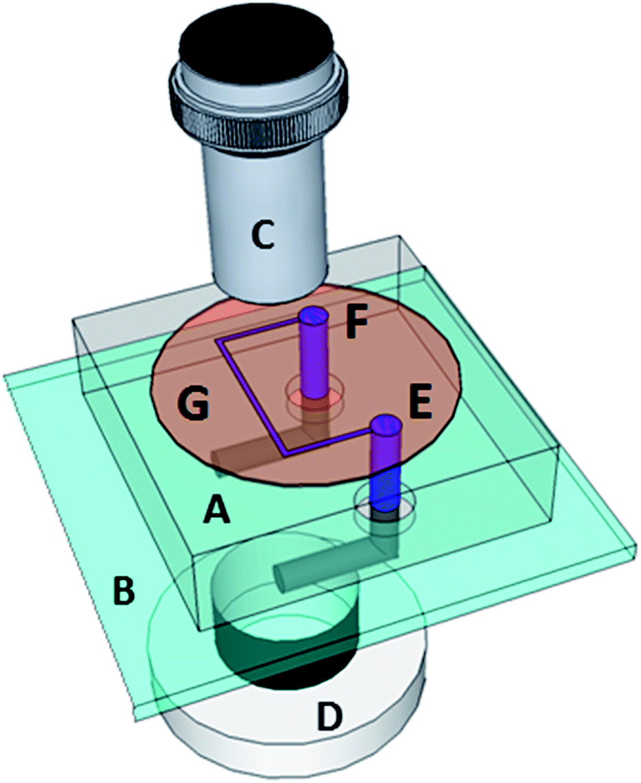 | ||
| Fig. 2 Three dimensional schematic of a microfluidic chip integrated with a Raman microscope. A chip (A) is sealed to a glass slide (B) with input and output ports (E and F), placed in between an objective (C) and condenser (D). The top part of the chip contains a system of channels and valves covered with CaF2/quartz (G). | ||
Raman z-scan through the microfluidic device
The high surface to volume ratio in a microfluidic chip may cause undesirable background noise in a Raman data set. A “z-scan” through the microfluidic chip, filled with water, was made to show the influence of each component of the chip for the Raman spectra at each z-position through the chip. The Raman spectra of quartz, water and PDMS are clearly distinguishable and have been used to investigate the contribution of a layer to the confocal plane of interest. The Raman spectra in the z-scan were taken every 0.2 μm along 200 μm. The data are presented in Fig. 3 as changes in the Raman signal intensity at various depths for the most prominent bands of PDMS at 488 cm−1, water at 3300–3700 cm−1 and the laser reflection at 0 cm−1. The data points in the graph are the calculated integrals for each band. The position of the laser focus in the microfluidic chip is represented by the blue curve. This curve shows the expected high reflected intensity when the laser is focused at the interface of the layers. The position of the layers in the chamber can be obtained in this manner. It also corresponds well with the water band intensity, which has a maximum signal contribution in the middle of the chamber. | ||
| Fig. 3 Comparison of the Raman signal intensity for selected bands of PDMS (488 cm−1: green curve), water (3300–3700 cm−1: black curve) and the laser reflection intensity (blue curve) through the microfluidic device. The top bar represents each layer and the corresponding refractive indexes in the microfluidic chip. The laser reflection (blue curve) maximizes at the interfaces. The curves for laser light intensity and water have been displaced for clarity. | ||
The very intense Raman signal of PDMS drops rapidly and contributes weakly when the confocal plane coincides with the aqueous medium in the chamber. The focal volume is approximately a spheroid with a smaller-to-longer axis dimension of 400 nm × 1500 nm, whereas the height of the channel is 18 μm. This distance is sufficient to decrease the intensity of the PDMS signal in the Raman spectrum of a cell adhered to the top window by about a factor of 10.
Cells in a microfluidic chip
Raman images were acquired of single cells in a fluidic channel. The images were obtained by stepping the laser every 0.1 s with 0.234 μm over an area of 225 μm2, which resulted in 4096 spectra in less than 7 minutes. The white light image and the cluster image of the cell with corresponding color coded Raman spectra are presented in Fig. 4. The nine cluster hierarchical cluster analysis (HCA) of the acquired Raman data set was performed. The images and the corresponding average cluster Raman spectra show that high-resolution images and high signal-to-noise ratio spectra can be acquired in the described microfluidic chip without any enhancement or labeling. The cluster Raman spectra present the composition of the cell in terms of important cellular compounds. Raman vibrations can be assigned to chemical compounds and groups, such as 1002 (phenylalanine), 1263 (amide III, collagen), 1300 (CH2 twisting, protein, collagen), 1442 (cholesterol band), 1656 (amide I), and 2852 (CH2 symmetric stretch).24 The background noise of PDMS and water is represented by the black cluster. Although the intense Raman bands of PDMS, e.g. 610 cm−1, 701 cm−1, 1259 cm−1 and 1409 cm−1, contribute to the Raman spectra of the cell, the amplitude is low and its negative contribution to the signal-to-noise ratio is minor. The orange and brown cluster spectra contain bands at 1575 cm−1 and 1092 cm −1, which are characteristic of DNA. These clusters represent the distribution of DNA in the nucleus. The red and dark green cluster spectra show an intense band at 1442 cm−1, assigned to cholesterol and lipids. The relative ratio of these two clusters varies and contrasts strongly with the cell membrane (magenta) and the cytoplasm (light green). The violet cluster is distinguished from the cell membrane and envelops the entire cell to connect to the cytoplasm (light green). A univariate image of the cell is presented in Fig. 4B. Each pixel represents the integrated Raman signal from the position of 1424–1473 cm−1, showing the distribution of cholesterol, lipids and proteins in the cell. The bright green region corresponds to the red cluster in Fig. 4C, which represents the highest concentration of cholesterol. | ||
| Fig. 4 (A) The white light image of a cell in the microfluidic channel through the quartz window. (B) A univariate image of the cell from the Raman intensity in the region of 1424–1473 cm−1. (C) A 9 cluster image of the cell. The image size of 15 μm × 15 μm was acquired with a step size of 234 nm, a time of 0.1 second per pixel and a laser power of 35 mW. (D) Color coded Raman cluster spectra corresponding to the colors in the image. The spectra were shifted vertically for clarity. | ||
z-Scans of the microfluidic chip were also acquired with a cell in the chamber. One z-scan was performed through the cell and one z-scan was performed next to the cell. Fig. 5 compares the Raman signal intensity of the NCI-H1650 cell and PDMS along the z-coordinate for each selected confocal plane in the chip. The data points are integral intensities calculated for chosen bands (see Fig. 4) for PDMS and the cell from the fingerprint region between 800 cm−1 and 1800 cm−1. The spectral region for the cell does not overlap with the signal of the PDMS. The obtained results show that in the middle of the chamber, the intensity of the PDMS signal is 4 times lower than that of the cell, and it is ∼zero before the confocal plane reaches the quartz surface.
 | ||
| Fig. 5 (A) Comparison of PDMS Raman signal intensity (black graph) and the cell in the microfluidics (blue line). (B–F) The 10 cluster cell images acquired with a step size of 270 nm every 2.5 μm from the quartz surface. Image area: 30 μm × 30 μm, time: 0.1 second per pixel, laser power: 35 mW. | ||
In addition, images of the cell were acquired every 2.5 μm in the z-direction. Images based on the hierarchical cluster analysis of the Raman data sets are presented in Fig. 5B–F. We performed ten-level cluster analysis for each image, which resulted in three clusters in image B and five clusters in images C to F. Clusters that belong to the background are presented as one color (black) for better visibility of the cell. The variation in the background is due to varying contributions of PDMS, water and quartz at different depths in the microfluidics, as can be observed from the z-scan in Fig. 5A. The cluster spectra connected to the cell distinguish variations in chemical composition, and it can be directly observed that a different distribution occurs at different confocal depths. Image B, acquired 8 μm from the quartz surface, shows only the bottom part of the cell and therefore does not contain all clusters. The green cluster contains the most intense bands at 1002 cm−1 (phenylalanine), 1263 cm−1 (amide III, collagen), 1300 cm−1 (CH2 twisting, protein, collagen), and 1442 cm−1 (cholesterol) in comparison with the rest of the clusters. The green cluster spectrum shows bands at 1575 cm−1 and 1091 cm−1, which can be assigned to DNA. The results show that 3D information on the chemical distribution in a single cell inside a microfluidic chip can be obtained.
Conclusion
We have designed, prepared and tested a microfluidic chip that enables the acquisition of high-resolution Raman images of a biological cell in a chip for the first time. The chip was adapted to the stringent requirements of high NA objectives, which are essential in high resolution Raman and, in general, optical imaging. The microfluidic channels were embedded in PDMS, which has a strong Raman spectrum that easily overwhelms information from biological cells. The careful design of the microfluidic chip, together with successful coupling to a confocal Raman microspectrometer, enables the acquisition of high spatial resolution Raman images of cells in both 2D and 3D measurement modes. The expected contribution of Raman scattering from other materials in the chip, such as PDMS, quartz or CaF2, has been minimized in this design. It was further shown that the chip can be filled with aqueous solution with or without cells without leakage, due to the sufficiently strong bonding of either CaF2 or quartz to PDMS through the plasma treatment of PDMS and the optimization of the fluid loading parameters.Acknowledgements
This work is part of the research program “Spectroscopic analysis of particles in water”, which is (partly) financed by Fundamenteel Onderzoek der Materie (FOM), which is financially supported by the Nederlandse Organisatie voor Wetenschappelijk Onderzoek (NWO). This work was performed in the cooperation framework of Wetsus, Centre of Excellence for Sustainable Water Technology. Wetsus is co-funded by the Dutch Ministry of Economic Affairs and Ministry of Infrastructure and Environment, the European Union Regional Development Fund, the Province of Fryslân, and the Northern Netherlands Provinces.Notes and references
- D. C. Duffy, J. C. McDonald, O. J. A. Schueller and G. Whitesides, Anal. Chem., 1998, 70, 4974–4984 CrossRef CAS PubMed.
- A. F. Chrimes, K. Khoshmanesh, P. R. Stoddart, A. Mitchella and K. Kalantar-Zadeha, Chem. Soc. Rev., 2013, 42, 5880–5906 RSC.
- D. Janasek, J. Franzke and A. Manz, Nature, 2006, 422, 374–380 CrossRef PubMed.
- W. Fritzsche and J. Popp, Optical Nano and Microsystems for Bioanalytics, Springer, Berlin, 2012 Search PubMed.
- J.-B. Salmon, A. Ajdari and P. Tabeling, Appl. Phys. Lett., 2005, 86, 094106 CrossRef PubMed.
- P. D. I. Fletcher, S. J. Haswell and X. Zhang, Electrophoresis, 2003, 24, 3239–3245 CrossRef CAS PubMed.
- A. E. Kamholz, E. A. Schilling and P. Yager, Biophys. J., 2001, 80, 1967–1972 CrossRef CAS.
- S. Leung, R. F. Winkle, R. C. R. Wootton and A. J. deMello, Analyst, 2005, 130, 46–51 RSC.
- K. W. Kho, K. Z. M. Qing, Z. X. Shen, I. B. Ahmad, S. S. Lim, S. Mhaisalkar, T. J. White, F. Watt, K. C. Soo and M. Olivo, J. Biomed. Opt., 2008, 13, 054026 CrossRef PubMed.
- F. Paquet-Mercier, N. Aznaveh, M. Safdar and J. Greener, Sensors, 2013, 13, 14714–14727 CrossRef CAS PubMed.
- A. J. deMello, Nature, 2006, 442, 394–402 CrossRef CAS PubMed.
- S. E. Barnes, Z. T. Cygan, J. K. Yates, L. Kathryn, E. J. Amis and B. Amis, Analyst, 2006, 131, 1027–1033 RSC.
- F. Sarrazin, J. B. Salmon, D. Talaga and L. Servant, Anal. Chem., 2008, 80, 1689–1695 CrossRef CAS PubMed.
- M. Knauer, N. P. Ivleva, R. Niessner and C. Haisch, Anal. Bioanal. Chem., 2012, 402, 2663–2667 CrossRef CAS PubMed.
- M. Fleischmann, P. J. Hendra and A. J. McQuillan, Chem. Phys. Lett., 1974, 26, 163–166 CrossRef CAS.
- J. Kneipp, H. Kneipp, A. Rajadurai, R. W. Redmond and K. Kneipp, J. Raman Spectrosc., 2009, 40, 1–5 CrossRef CAS PubMed.
- X. Zhang, H. Huabing, J. M. Cooper and S. J. Haswell, Anal. Bioanal. Chem., 2008, 390, 833–840 CrossRef CAS PubMed.
- C. D. Syme, N. M. S. Sirimuthu, S. L. Faley and J. M. Cooper, Chem. Commun., 2010, 46, 7921–7923 RSC.
- Y. Xia and G. Whitesides, Annu. Rev. Mater. Sci., 1998, 28, 153–184 CrossRef CAS.
- V. V. Pully, A. Lenferink and C. Otto, J. Raman Spectrosc., 2010, 41, 599–608 CrossRef CAS PubMed.
- N. Uzunbajakava, A. Lenferink, Y. Kraan, E. Volokhina, G. Vrensen, J. Greve and C. Otto, Biophys. J., 2003, 84, 3968–3981 CrossRef CAS.
- N. Uzunbajakava, J. Greve and C. Otto, Multiphoton Microscopy in the Biomedical Sciences III, 2003, pp. 223–230 Search PubMed.
- D. Mazia, G. Schatten and W. Sale, J. Cell Biol., 1975, 66, 198–200 CrossRef CAS.
- Z. Movasaghi, S. Rehman and I. U. Rehman, Appl. Spectrosc. Rev., 2007, 42, 493–541 CrossRef CAS PubMed.
| This journal is © The Royal Society of Chemistry 2015 |