Sayantan Mazumdar and
Aninda J. Bhattacharyya*
Solid State and Structural Chemistry Unit, Indian Institute of Science, Bangalore-560012, India. E-mail: aninda_jb@sscu.iisc.ernet.in; Fax: +91 8023601310
First published on 10th April 2015
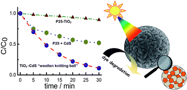
An unprecedented morphology of a titanium dioxide (TiO2) and cadmium sulfide (CdS) self-assembly obtained using a ‘truly’ one-pot and highly cost effective method with a multi-gram scale yield is reported here. The TiO2–CdS assembly, comprising of TiO2 and CdS nanoparticles residing next to each other homogeneously self-assembling into ‘woollen knitting ball’ like microspheres, exhibited remarkable potential as a visible light photocatalyst with high recyclability.
Sensitization of titanium dioxide by another light harvesting semiconductor of lower band gap (around ∼2 eV) is a very effective approach and has assumed great relevance in several photochemical applications.10 Among various low band gap (≈2 eV) semiconductors, cadmium sulphide (II–VI semiconductor) has proven to be one of the most viable candidates owing to its unique electronic band structure.11 The position of its conduction band edge is higher than that of titanium dioxide (even in the bulk) and as a result, favourable electron injection rates from the CdS to TiO2 on ultrafast timescale can be achieved.12 CdS also facilitates ease of synthesis due to its higher stability and yield compared to the other competitors like CdSe or CdTe. The effective electronic properties of the assembly of the wide and narrow band gap semiconductor can be additionally tuned by tailoring their geometry and spatial configuration at the nanoscale.1h,10c,12 Attachment of the light harvester to the wide band gap semiconductor is also observed to be a key issue, as this, along with nanostructuring greatly affects the electron transfer kinetics and hence photochemical property of the semiconductor assembly.12 Thus, the abundance and low cost of a TiO2–CdS assembly with efficient electron transfer properties will be in great demand not only for the much discussed third generation photovoltaics but also for photocatalysis for spectral range wider than UV-regime. Approaches have been devised towards facile synthesis of TiO2–CdS heterostructures for visible light photocatalysis and other related applications. In few cases, the synthesis involved multiple steps and the photocatalytic ability is not satisfactory.2g–j Zhao et al. reported a TiO2–CdS heterostructure via a one-step solvothermal method with enhanced photocatalytic activity.2i However, the stability and reusability of the photocatalyst, which is a very vital issue for a photocatalyst for practical applications, was not reported.
In this work, a TiO2–CdS nano-heterostructured assembly has been synthesized using a very facile and ‘truly’ one-pot synthesis method. The synthesis method yielded products in multi-gram scale quantity which is the necessary desired goal for any practical and industrial mass scale applications. The often much highlighted issue of toxicity associated with cadmium is easily tackled here by the remarkable stability and recyclability of the TiO2–CdS assembly.
In a typical synthesis, a CdS precursor (e.g. L-cysteine as the S-precursor, cf. Experimental section) along with a surfactant, (acting as the structure directing agent) are taken in a teflon container in a water–ethanol mixture. TiO2-precursor is then added to the CdS-precursor–water–ethanol mixture and hydrolysed using acid. Solvent is evaporated by constant stirring. Subsequently, di-methyl formamide is added to the CdS precursor–surfactant–TiO2-precursor mixture which was then subjected to a solvothermal reaction (cf. Experimental section). The orange-yellow product is centrifuged, washed with water and ethanol and then dried in vacuum under mild heating condition.
The dried product is subjected to further experimental investigations. Systematic investigations using scanning electron microscopy vividly reveal as synthesized products constituting of micrometre sized spheres (diameter ≈ 1 μm). These microspheres were in turn composed of nanometre sized particles of TiO2 and CdS. Two of the representative SEM images are shown in Fig. 1(a) and (b). The microspheres are observed to be ∼1–2 μm in diameter and mimic a ‘woollen knitting ball’. Identical types of ‘woollen knitting balls’ are found at various scanned areas of the sample along with few aggregates and smaller size spheres (cf. Fig. 1(d) and S1†). HRTEM on various parts of a single sphere and repeated on various microspheres reveal that anatase TiO2 and mixed-phase CdS nanoparticles of very small size (∼5 nm) reside very close to each other in a side by side configuration over the entire microsphere. For TiO2 and CdS, the (101) plane is clearly visible. This is exactly identified by the interplanar spacing for anatase TiO2 (d101 ≈ 0.352 nm) and wurtzite CdS (d101 ≈ 0.316 nm). The residence of TiO2 and CdS nanoparticles next to each other can be seen very clearly in Fig. 1(e) and S1.† The observation of side by side residence of TiO2 and CdS is also supported by elemental mapping of microspheres done via energy-dispersive X-ray spectroscopy (EDS) done on the same microsphere as shown in Fig. 1(a). The EDS shows a homogeneous distribution of all the constituent elements viz. Ti, O, Cd and S throughout the microsphere as demonstrated by the elemental mapping in Fig. 1(f). Both the constituents i.e. TiO2 and CdS showed high crystallinity at the nanometer scale as evidenced by the clear visibility of the planes in the HRTEM images. In few cases, (101) planes from anatase TiO2 and wurtzite CdS are overlapped to form Moiré patterns which confirm good crystallinity as well as homogeneous distribution of both TiO2 and CdS in all directions (cf. Fig. 1(e) and S1†). TiO2 nanoparticles are formed under solvothermal conditions in an acidic medium and their growth is restricted by the surfactant (CTAB) present in the reaction mixture. CdS nanoparticles form due to reaction of Cd2+ and S2− precursors during the solvothermal reaction in presence of the high boiling point DMF solvent. Simultaneous formation of TiO2 and CdS nanoparticles leads to a micro-sized spherical assembly where both of them reside next to each other. Presence of water and ethanol has a effect on the “woolen-knitting ball” like morphology. When the same reaction is carried out in the presence of DMF (i.e. in the absence of water and ethanol), microspheres formed but it does not resemble a “woolen knitting ball” like morphology. The surface characteristics appeared to be different (cf. Fig. S2†) compared to as shown in Fig. 1(a) and (b).
The crystalline nature of the TiO2–CdS assembly is also visible in the powder XRD pattern in Fig. 2(a) where all the peaks are indexed to either anatase TiO2 (JCPDS 21-1272) or predominantly to wurtzite CdS (JCPDS 41-1049). The mixed-phase nature of CdS is evidenced via the observation of a small peak at 2θ = 30.7° (indicated by an arrow in Fig. 2(a)) assigned to the zinc blende CdS (200) phase (JCPDS 80-0019). It is worth mentioning that the zinc blende (200) is the only significant peak for the zinc blende CdS which doesn't overlap with any of the wurtzite CdS peaks. The mixed phase nature of CdS is also evidenced from the SAED pattern shown in Fig. 2(b). Presence of kinetically favourable zinc blende phase is generally expected as the reaction has been carried out in a mixed solvent media solvothermally at low temperature.10c,13 The BET surface area of the TiO2–CdS sample is found to be 66 m2 g−1 (cf. Fig. S3†). Interestingly, the BJH pore distribution (cf. Fig. S4†) reveals a microporous morphology (distribution maximum < 2 nm) for the TiO2–CdS assembly.
Steady state optical property is studied via absorbance and photoluminescence spectroscopy for the as synthesized TiO2–CdS assembly, a wurtzite CdS sample and an equimolar mixture of the same wurtzite sample with commercially available Degussa P25-TiO2. The wurtzite CdS sample, P25-TiO2 and an equimolar mixture of P25-TiO2:CdS were used as the benchmark materials to compare the properties with the as synthesized TiO2–CdS assembly. Both of the samples exhibit onsets at similar wavelengths, the wurtzite CdS sample has a slightly broader absorption spectrum than the TiO2–CdS assembly (cf. Fig. 3). The optical band gap estimated from the Kubelka–Munk plots are 2.32 eV and 2.15 eV for TiO2–CdS assembly and CdS respectively. The P25–CdS sample absorption spectrum matches exactly with the wurtzite CdS sample. The band gap of the TiO2–CdS assembly is smaller than that of bulk CdS value (=2.42 eV), which is not unexpected in mixed-phase CdS nanomaterials.10c
Fig. 3 Absorbance spectra of TiO2–CdS microsphere assembly (TC) and wurtzite CdS, the Kubelka–Munk plots to measure the direct band gap are in inset. |
Photoluminescence behaviour of the samples is also measured. In general, all the three samples exhibited broad emission characteristics however, the profiles were distinctly different for the TiO2–CdS assembly compared to the other two samples (Fig. 4). The P25–CdS sample displayed a PL spectrum similar to the CdS but with lesser intensity compared to the CdS sample. This attributed to the transfer of electrons from conduction band of CdS to the conduction band of TiO2. The TiO2–CdS assembly displayed much lower intensity in the PL spectrum than the P25-TiO2:CdS sample. Higher quenching of PL in the nano-heterostructured TiO2–CdS assembly suggests a more favourable kinetics for electron transfer from the conduction band of CdS to the conduction band of TiO2 compared to the physical mixture of CdS and P25-TiO2.1h,14
Fig. 4 Photoluminescence spectra of TiO2–CdS microsphere assembly (TC), wurtzite CdS, wurtzite CdS:P25-TiO2 mixture. |
Fig. 5 shows the dye degradation profiles for TiO2–CdS assembly, abbreviated hereafter as TC. Recently, Choi et al. pointed out that the photocatalytic activity of a photocatalyst may be dye-specific and dye-degradation tests on multiple dyes rather than on a single one is prescribed to evaluate the intrinsic photocatalytic property of a material.15 Based on this observation, photocatalytic activity of TC were performed on three separate dyes, namely methylene blue (MB) (a phenothiazine-cationic dye which is highly recommended due to its minimal absorption spectral overlap with the visible light photocatalyst and dye sensitization effect), indigo carmine (IC) (anionic dye) and rhodamine B (xanthene–Zwitter ionic dye). The absorption spectra were collected over a wide wavelength range (300 to 900 nm) using aliquots taken out at every 5 min intervals. This was done to monitor the formation of the degraded products rather than mere dye-mineralization. No other peaks other than that those related to the particular dye under investigation was observed. Fig. 5(a) depicts the degradation profiles of the MB dye due to TC and other samples. The degradation of IC and RhB by TC are also plotted in the same figure for comparison of the photocatalytic activity of TC. Fig. 5(b) shows only the degradation profiles of the dye IC. Sample TC is observed to be highly efficient and is able to degrade MB to one fifth of the starting concentration under 20 minutes. The degradation profile follows apparent first-order kinetics which is strongly evident from the one-exponential decay curve (Fig. 5(c)). In comparison, the Degussa P25 exhibited very poor efficiency towards MB dye degradation. This is clearly due to poor light harvesting properties of the pristine TiO2 under visible light. Due to wide band gap (=3.2 eV), TiO2 is predominantly activated under UV light which is only 4–5% of the total light.1b,c,4 As a consequence, only a few electrons can be excited and the dye degradation is poor. The MB degradation by the wurtzite CdS sample is much slower than that of TC and it slightly improves when it's mixed with P25-TiO2 (cf. Table 1). TC is observed to be even more effective in degrading the IC dye, 90% of the dye solution degraded in 15 minutes. In case of degradation of IC as well, similar trends were observed with regard to the reference samples (wurtzite CdS and P25-TiO2–CdS). Degradation of IC by CdS sample is less efficient than TC and improves marginally when mixed with P25-TiO2. Fig. 5(a) and (b) also shows the degradation kinetics of the dyes in the absence of any semiconductor. On its own, the degradation of MB and IC dyes is negligible. This strongly suggests that the observed change in concentration as a function of time is not merely due to dye changes but rather to the degradation action induced by the TiO2–CdS nano-heterostructure. The microspheres exhibit excellent reproducibility over few tens of cycles. This is evidenced from the photocatalytic efficiency obtained following several cycles (cf. Fig. S7†). The nominal loss of photocatalytic activity over successive cycles may be attributed to the loss of the photocatalyst occurring during each round of retrieval, rinsing and transfer to the reaction vessel. The SEM images recorded as a function of the photocatalytic cycles showed similar profile after each cycle (cf. Fig. S7†) and the elemental maps also suggested no change in the nano-heterostructure.
Sample | Dye | k (min−1) |
---|---|---|
TC | Methylene blue | 0.085 |
CdS | MB | 0.035 |
P25 | MB | 0.01 |
P25 + CdS | MB | 0.046 |
TC | Indigo carmine | 0.13 |
CdS | IC | 0.071 |
P25 | IC | 0.022 |
P25 + CdS | IC | 0.078 |
TC | Rhodamine B | 0.06 |
The recyclability of the P25-TiO2:CdS sample was also monitored (cf. Fig. S8†). However, a significant loss of photocatalytic activity is observed immediately after the first cycle due to photo-corrosion. Though photo-corrosion is a major concern of CdS photocatalysts, it can be eliminated by synthesizing optimized heterostructures where charge transfer from CdS to the other moiety can be easily facilitated. This leads to excellent stability and reusability.2a In our case, the tailored heterostructure prohibits any kind of corrosion of the photocatalyst as well as preserves the homogeneity even at nanometre length scale, thus facilitating efficient charge transfer from CdS to TiO2 at various cycles. Hence, such semiconductor assemblies bear great promise for practical industrial applications. Apparent first order kinetics rate constant are estimated to be, k = 0.085 (±0.001) min−1 for degradation of MB by the sample TC and k = 0.13 (±0.016) min−1 for degradation of IC which are two order higher than the commercial TiO2 (∼0.001 min−1 for Degussa P25), almost double than that of the P25–CdS sample and several order higher compared to photocatalysis in absence of any semiconductor. The excellent degradation activity of TC can be attributed to better electron injection from the light harvester CdS to TiO2. This result is also remarkable in the context of photocatalyst comprising of Au-tagged TiO2. Though the rate constant is slightly higher [kAu–TiO2 = 0.25 min−1]7c than that of TC, the slight inferior performance is offset by the cost effectiveness of the ‘truly’ one pot multi-gram synthesis from abundant materials employed here. The superior electron injection rate in case of TC is also strongly supported by the PL data which exhibits lesser emission than sample P25–CdS. As highlighted earlier, the interface characteristics here also plays an important role. The microporous nature of the sample and higher surface area also support it to gain an excellent photocatalytic activity under visible light (Scheme 1).
Scheme 1 Schematic depiction of dye degradation by nano-heterostructured TiO2–CdS assembly under visible light. Reactive oxygen species is abbreviated as ROS. (E0 O2 (aq.)/O2˙ = −4.34 eV). (pH ≈ 7). |
Footnote |
† Electronic supplementary information (ESI) available: More SEM and HRTEM images, BET, BJH, N2 adsorption–desorption isotherm, XPS, recyclability of the TiO2–CdS microsphere assembly and the benchmark sample as a photocatalyst. See DOI: 10.1039/c5ra04733a |
This journal is © The Royal Society of Chemistry 2015 |