Effects of rapid thermal annealing on the properties of AlN films deposited by PEALD on AlGaN/GaN heterostructures

Duo Caoabd, Xinhong Cheng*a, Ya-Hong Xieb, Li Zhengabd, Zhongjian Wanga, Xinke Yub, Jia Wangb, Dashen Shenc and Yuehui Yua
aState Key Laboratory of Functional Materials for Informatics, SIMIT, Chinese Academy of Sciences, Changning Road 865, Shanghai 200050, P. R. China. E-mail: xh_cheng@mail.sim.ac.cn
bDepartment of Materials Science and Engineering, University of California, Los Angeles, California 90095, USA
cDepartment of Electrical and Computer Engineering, University of Alabama in Huntsville, Huntsville, Alabama 35899, USA
dUniversity of Chinese Academy of Sciences, Beijing 100049, P. R. China

Received 17th March 2015 , Accepted 21st April 2015

First published on 21st April 2015


Abstract

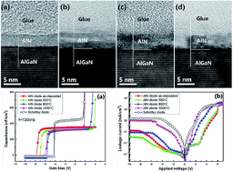
Aluminum nitride (AlN) films have been deposited on AlGaN/GaN heterostructure substrates by plasma enhanced atomic layer deposition (PEALD). Different annealing treatments were adopted to change film structure and improve performance. Chemical composition, crystallinity, and electrical properties were studied for AlN films. The results show that some crystal grains appear in the films after annealing at a temperature of over 800 °C. The film crystalline quality increases as the annealing temperature rises. The N–O–Al bond decomposes during the high temperature annealing in N2, and some new N–Al bonds are formed in the AlN films. Annealing promotes the elemental interdiffusion between the films and the substrates. High-temperature annealing at 1000 °C in a nitrogen atmosphere can effectively promote complete nitridation of the AlN film, reduce the nitrogen vacancies, and cause the AlN film to form a semiconductor-like structure.


Introduction

III-nitride semiconductors are extensively used in power electronic and optoelectronic devices. In particular, aluminum nitride (AlN), with high thermal conductivity (320 W m−1 K−1 at 300 K), wide direct band gap (Eg = 6.2 eV), high electrical resistant (1013 Ω cm), high fusion temperature (2400 °C) and high chemical stability, extends the application of the III-nitrides to high temperature and high power field.1–5 Furthermore, because of the relatively close match between the lattice constants and thermal properties of AlN and GaN, AlN is typically used as a buffer layer for GaN-based devices where low defect structures are needed. AlN is also a leading candidate to replace sapphire, Si, and SiC as a commercial substrate for nitride-based microelectronics applications.2,6 As a result of these material properties, a significant amount of research has been devoted to the growth and characterization of AlN thin films.7–9 In addition, rapid thermal annealing (RTA) can be used for improving the crystal structure of crystalline material. In the case of III-nitrides it may balance the fluctuations of nitrogen concentration and reduce crystal defects generated during the growth of the layer. Thermal annealing gives energy to atoms for rearranging and the grains in polycrystalline material start to grow and smaller grains can merge into larger ones, and all these greatly affect the film quality and property.10,11

While high-temperature (above 1000 °C) epitaxial grown AlN films are used in active electronic and opto-electronic device layers, polycrystalline and amorphous AlN films grown at CMOS-compatible temperatures (not higher than 300 °C) are widely used as dielectric and passivation layers for microelectronic devices.12 Recently plasma enhanced atomic layer deposition (PEALD) method has been proved to be a promising growth technique. With its self-limiting digital growth mechanism, PEALD offers the opportunity to create precisely controlled thickness but is rarely used to grow AlN.13 Moreover, the in situ plasma used in PEALD also facilitates low-damage pretreatment and remove the surface native oxide with minimum surface damages. The in situ pre-passivation surface treatments by plasma such as NH3 has been shown to result in improved reliability in SiNx-passivated AlGaN/GaN HEMTs.14 However in those reports about ALD AlN, either AlN used as a passivation layer is observed15,16 or research was only focused on the structural properties of the AlN films.4,6,17 Clearly, however, detailed annealing effect on the structural and electrical properties of AlN is needed to be more firmly established.

In this work, we investigated the properties and temperature effects on the AlN films grown on AlGaN/GaN heterostructures by PEALD. Films were treated with RTA at a series of annealing temperatures. The micro-structures and electrical performance of the films were presented in detail. Ni–Au/AlN/AlGaN/GaN MIS diodes were designed to measure the electrical properties of the AlN films.

Experimental

Si-based GaN wafer was chosen, where 3.9 μm GaN (0001) buffer, 20 nm undoped Al0.25Ga0.75N barrier, and 2 nm GaN cap were grown on Si (111) by metal organic chemical vapor deposition (MOCVD). The wafer was cleaned with acetone to remove organic contamination, and rinsed with deionized water. After blown dried in N2, the samples were immediately loaded into the PEALD reactor. Trimethyl aluminium Al(CH3)3 (TMA) and ammonia (NH3) enhanced by RF-plasma were used as precursors while Ar was used as the carrier gas. Al(CH3)3 was manufactured in Nanjing University, and was with a purity of 99.99+%. Precursor was delivered to the chamber with Ar carrier gas at a flow rate of 100 standard cubic centimeters per minute (sccm). Ultra-high purity grade NH3 with a flow rate of 60 sccm was used to offer nitrogen. Ar with a flow rate of 40 sccm was used as the purge gas. TMA pulse of 0.2 s was introduced first, then the NH3 plasma was generated for 2 s, and the Ar purged the reactor for 5 s. To ensure consistency, all samples were deposited by PEALD at 300 °C with in situ pre-NH3 and pre-Ar plasma treatments, the plasma RF power being 75 W. The growth rate of AlN is ∼0.07 nm per cycle, which is determined by spectroscopic ellipsometry and transmission electron microscopy of previous experiments. This growth rate is close to 0.06 nm per cycle reported by Huang et al.18 For our AlN films, 70 cycles were grown. MIS structures on the substrate of AlGaN/GaN/Si were fabricated, where a part of the wafer was shielded to avoid the growth of AlN film. The shielded area was used for making ohmic contact. The sizes of the anode and cathode were 7.9 × 10³ and 1 × 108 μm2, respectively. The cathode was formed by e-beam evaporation of Ti/Al/Ni/Au (20 nm/100 nm/50 nm/100 nm). Then RTA at 870 °C in the nitrogen atmosphere for 30 seconds was used to form the ohmic contact. After the PEALD process, selected samples were treated by RTA in N2 at 500 °C for 1 min, 800 °C for 1 min or 1000 °C for 1 min, respectively. Subsequently the anode was formed through Ni/Au (30 nm/100 nm) deposition on AlN. Post metallization annealing (PMA) was performed in a 95% N2 and 5% H2 mixed atmosphere at 400 °C for 3 minutes to improve the interface between the dielectric film and Ni/Au. Given that AlN film is easily oxidized when exposed to air at a high temperature,19 we ensure that each time the samples are cooled to room temperature before taken them out of the PEALD or RTA chambers.

Results and discussion

A CM200FEG instrument was used for high-resolution transmission electron microscopy (HRTEM). Fig. 1(a)–(d) shows the HRTEM cross-section images of AlN films deposited on AlGaN/GaN prepared by PEALD and by RTA at different temperatures. The as-deposited film shows a totally amorphous structure, as is shown in Fig. 1(a). The film is getting a little thicker after annealing, mainly due to the elemental interdiffusion between the films and the substrates. The physical thicknesses of the AlN films are determined to be 4.1, 5.2, 5.0 and 4.9 nm, respectively. As is shown in Fig. 1(c) and (d), the AlN films are partially crystallized. Some crystal grains exist within the AlN layers after annealing at a higher temperature, and it is especially evident in the 1000 °C annealed AlN sample. The results reveal that as the annealing temperature rises, the degree of film crystallinity increases.
image file: c5ra04728e-f1.tif
Fig. 1 Cross-sectional HRTEM micrographs of the AlN films deposited on the AlGaN/GaN heterostructures with different annealing conditions, (a) as-deposited, (b) RTA in N2 at 500 °C for 1 min, (c) RTA in N2 at 800 °C for 1 min, and (d) RTA in N2 at 1000 °C for 1 min.

In order to analyze the phases of the crystals in the film, we carried out the in-plane grazing incidence X-ray diffraction (GIXRD) measurements. The measurement was carried out at the Department of Materials Science and Engineering in UCLA. The X-ray wavelength was 0.154 nm and the X-ray beam was incident at a grazing angle of 0.5°. Fig. 2 shows the GIXRD patterns for the AlN films annealed at different temperatures. The profiles from both the as-deposited and 500 °C annealed samples show no peak, indicating their amorphous nature, while the profiles from the samples with higher temperature annealing show obvious diffraction peaks indicating their crystalline phases. This is in good agreement with the results given by HRTEM. The thin films with 800 °C and 1000 °C annealing exhibit prevalence of a polycrystalline hexagonal AlN structure perfectly matching with the XRD Bragg diffraction peak positions corresponding to the literature.17,20 GIXRD patterns reveal that the film crystalline quality increases as the annealing temperature rises.


image file: c5ra04728e-f2.tif
Fig. 2 GIXRD patterns for the AlN films deposited on the AlGaN/GaN heterostructures. The profiles from the as-deposited and 500 °C annealed samples both show no peak, indicating their amorphous nature, while the profiles from the films with 800 °C and 1000 °C annealing exhibit prevalence of a polycrystalline hexagonal AlN structure.

X-ray photoelectron spectroscopy (XPS) was performed with an Axis Ultra DLD equipment to analyze chemical binding states, using Al Kα radiation. The binding energy (BE) was calibrated to the position of the C 1s peak at 284.8 eV. Fig. 3 shows the Al 2p, N 1s and O 1s core level spectra for the different annealed samples to compare the Al, N and O chemical bonding states in the AlN films. The Al 2p XPS scan obtained from the film surface is fitted by two subpeaks located at 73.8 and 74.7 eV, corresponding to Al–N (ref. 21 and 22) and Al–O (ref. 21 and 23) bonds, respectively. The Al–O peak attenuates relatively as the annealing temperature rises, which indicates the Al–O content decreases during the RTA in a N2 atmosphere. No Al–Al bonds that would appear at 72.9 eV can be found. The N 1s scan is fitted using three subpeaks located at 394.0, 396.5 and 398.6 eV. The peaks located at 396.5 and 398.6 eV are assigned to the N–Al and N–O–Al bonds,24 respectively, whereas the peak located at 394.0 eV is identified as the Auger Ga peaks,17,25 which is from the AlGaN substrate. The three-component system of N–O–Al is generally referred to as aluminum oxynitride (AlOxNy), which will be decomposed into Al–N and Al–O under a high temperature.19 The N–O–Al peak is observed to decrease in intensity as the annealing temperature increases, where the peak disappears at a higher annealing temperature of above 800 °C. Meanwhile, the N–Al peak strengthens and sharpens as the annealing temperature increases. Thus, we can conclude that the N–O–Al decomposes during the high temperature annealing in N2, and some new N–Al bonds are formed in the AlN films. The O 1s XPS scan is fitted by two subpeaks located at 531.1 and 532.6 eV, corresponding to O–Al (ref. 21 and 22) and Al–OH, O–C (ref. 21 and 26) bonds, respectively. These samples are not intentionally oxidized, but XPS detects traces of oxygen and carbon. In this case, the unintentional oxygen incorporation is either due to the oxidation of the AlN film by H2O and O2 during air exposure after film growth or O2 remains in the chamber as a residual gas during film deposition. During the deposition process, this residual oxygen or water can react with the aluminum to form Al–O or Al–OH near the surface of the AlN film. The peak located at 532.6 eV is observed to decrease in intensity as the annealing temperature increases, and this is due to high-temperature annealing will promote the dehydration reaction, turning Al–OH into Al–O.


image file: c5ra04728e-f3.tif
Fig. 3 XPS core level spectra of the Al 2p, N 1s, and O 1s spectral regions of the AlN films deposited on the AlGaN/GaN heterostructures with different annealing conditions.

The valence band (VB) spectra were measured for the AlN films grown on AlGaN/GaN, as well as the bulk AlGaN/GaN substrate. The measurement is based on the assumption that the energy difference between the core level and VB edge of the AlGaN/GaN substrate remains constant with/without the deposition of AlN.27 Fig. 4 shows the VB spectra of AlGaN/GaN substrate and different annealed AlN/AlGaN/GaN samples. The VB offset can be determined through valence band spectra of AlN/AlGaN/GaN samples and bulk AlGaN/GaN samples. The core level positions and VB maximum of the bulk materials combined with the core level difference of the heterojunction are used to calculate the VB offset. The VB maximum is determined by using a linear extrapolation method.27 In this case, the VB offset is approximately equal to the difference of the linear extrapolation intercept between AlN/AlGaN/GaN samples and bulk AlGaN/GaN samples. As is shown in Fig. 4, the VB offset of the as-deposited and annealed AlN samples are determined to be 1.2, 0.9, 0.5 and 0.1 eV. We can see that as the annealing temperature rises, the VB offset between the AlN and the substrate gets smaller and smaller, even falls to 0.1 eV when annealed at 1000 °C. This is mainly due to the elements diffusion during the high-temperature annealing. Annealing can improve the crystal structure of AlN, balance the fluctuations of nitrogen concentration and reduce crystal defects generated during the growth of the layer. In the case of 1000 °C annealed AlN, high temperature annealing gives energy to the Al, N, Ga atoms for rearranging, the AlN crystals start to grow on the surface of the substrate in a direction matching with the AlGaN lattice, which can be seen in Fig. 1(d). In this circumstance, the AlN seems more likely to be a semiconductor, which has similar properties to the AlGaN.


image file: c5ra04728e-f4.tif
Fig. 4 Valence band spectra for AlGaN/GaN substrate and different annealed AlN/AlGaN/GaN samples. The VB offset is approximately equal to the difference of the linear extrapolation intercept between AlN/AlGaN/GaN samples and bulk AlGaN/GaN samples.

To further investigate the elements depth distribution, we carried out the TEM energy dispersive X-ray spectroscopy (EDS) measurements. Atomic profiles of Ga–L, O–K, N–K, and Al–K with increasing depth for the AlN annealed at 500 °C and 1000 °C are shown respectively in Fig. 5. No major difference is observed in the Ga profile for both samples. Broad concentration peak values appear at the site of AlN layers in all the profiles of O, N and Al from both samples. The peaks of the O, N and Al profiles tend to be weaker and broader after annealing at a higher temperature of 1000 °C, which indicates that a higher temperature annealing promote the O, N and Al from both the AlN film and the substrate diffuse into each other, getting the elements of AlN/AlGaN structure more uniformly distributed. This is in good accordance with the results of the valence band analysis. The N atomic concentration at the upper portion of the 500 °C annealed AlN film is 19%, it increases to 33% in the 1000 °C annealed film. This indicates that the as-deposited AlN film tends to be lack of nitrogen, some nitrogen vacancies exist in the film, and high-temperature annealing in a nitrogen atmosphere can effectively promote complete nitridation of the AlN film.


image file: c5ra04728e-f5.tif
Fig. 5 EDS depth analysis for the AlN/AlGaN/GaN structures annealed at 500 °C and 1000 °C. The peaks of the O, N and Al profiles tend to be weaker and broader after annealing at a higher temperature of 1000 °C, which indicates that a higher temperature annealing promote the O, N and Al from both the AlN film and the substrate diffuse into each other, getting the elements of AlN/AlGaN structure more uniformly distributed.

The capacitance–voltage (CV) and leakage current–voltage (JV) of MIS capacitors were characterized using an Agilent B1505A Precision LCR Meter at 100 kHz. Fig. 6(a) shows CV characteristics of AlGaN/GaN Schottky diode and the AlN/AlGaN/GaN MIS diodes. A significant flat band voltage drift indicates a large interface fixed charge density. According to the EDS analysis, nitrogen vacancies with positive electrical charges existed in the AlN film, which would contribute to the positive fixed charge density. And high-temperature annealing in N2 can effectively reduce the nitrogen vacancies in the AlN film, reducing the positive fixed charges. As a result, as shown in Fig. 6(a), the flat band has positive shift as the annealing temperature rises. In addition, an increase in capacitance is observed at gate bias beyond +2 V. This is due to a charge spillover from the two-dimensional electron gas (2DEG) channel, which brings some of the carriers closer to the surface, thus decreasing the barrier layer effective thickness and increasing the capacitance. It can be observed that there is a negative shift in spillover voltage as the annealing temperature rises. Moreover, it even decreases to the same voltage with the Schottky diode after annealed at 1000 °C. This indicates that the 1000 °C annealed AlN form a somewhat semiconductor-like structure with small resistance which shares very little voltage with the AlGaN layer. This is in good agreement with the previous VB and EDS analysis. The 2DEG accumulation region capacitance of Schottky diode is 440 nF cm−2, and the capacitances of the AlN MIS diodes with increasing annealing temperatures are extracted to be 351, 327, 326 and 318 nF cm−2, respectively. According to series capacitance equation in the 2DEG accumulation region 1/CMIS-diode = 1/CSch-diode + 1/CAlN, the capacitance of the four AlN films are determined to be 1743, 1273, 1271 and 1152 nF cm−2, respectively. Given the films thickness determined by HRTEM, the dielectric constant of the AlN films are deduced to be 8.1, 7.5, 7.2 and 6.4. This result is similar to the report by Eom et al., where the dielectric constant of the as-deposited AlN is 7.9.28 The dielectric constant decline a bit as the annealing temperature rises, and this is due to more Al–N (AlN has smaller dielectric constant than Al2O3) formed after higher temperature annealing. This is corresponded with the XPS analysis. Fig. 6(b) shows JV characteristics of AlGaN/GaN Schottky diode and the AlN/AlGaN/GaN MIS diodes. The thin AlN layer can only reduce leakage current density at negative (V = −8 V) and forward bias (V = 2 V) by a maximum of 3 orders of magnitude, compared with Schottky diode. Both the negative and forward leakage current tend to increase as the annealing temperature rises. It is obvious that the 1000 °C annealed AlN sample has a remarkable increase of the leakage current compared with the other AlN MIS diodes. It is worth noting that the 1000 °C annealed AlN sample has similar JV profile with the Schottky diode, which also deduces that the 1000 °C annealed AlN film has a small resistance and the high-temperature annealing gives energy to the atoms for rearranging, forming a semiconductor-like structure. This is corresponded with the VB analysis result. The VB offset between the 1000 °C annealed AlN and the substrate is only 0.1 eV, which is a very small barrier for the electrons to transmit. In addition, Fig. 6(c) shows the turn-on voltage (Von) characteristics of AlGaN/GaN Schottky diode and the AlN/AlGaN/GaN MIS diodes. The Von is defined as intercept of the linear extrapolation of the leakage leading edge to the background level under linear scale. The Von of the AlN diode gets smaller as the annealing temperature rises. This also indicates that as the annealing temperature rises, the difference between the AlN film and the AlGaN gets smaller and smaller.


image file: c5ra04728e-f6.tif
Fig. 6 (a) CV characteristics of AlGaN/GaN Schottky and AlN/AlGaN/GaN MIS diodes, (b) JV characteristics of AlGaN/GaN Schottky and AlN/AlGaN/GaN MIS diodes, and (c) comparison of Von between AlGaN/GaN Schottky and AlN/AlGaN/GaN MIS diodes.

Conclusions

In summary, we have studied the effects of rapid thermal annealing on the properties of AlN films deposited by PEALD on AlGaN/GaN heterostructures. The structural properties are significantly affected by the annealing conditions. Hexagonal AlN structures appear after annealing at a temperature of above 800 °C. High temperature annealing in N2 breaks the N–O–Al bonds and forms N–Al bonds. It is worth noting that the annealing in N2 is a good way to suppress the Al–O bonds and improve the purity of AlN. The 1000 °C annealed AlN film has a small resistance and the high-temperature annealing gives energy to the atoms for rearranging, causing the AlN film to form a semiconductor-like structure. The PEALD-AlN films reveal some electrical properties with permittivities of 6.4–8.1, turn-on voltages of 3.0–5.9 V, and leakage of 0.01–10 mA cm−2 at a gate bias of Vg = −10 V.

Acknowledgements

This work was supported by the National Scientific Foundation of China (Grant no. 11175229). The authors gratefully acknowledge Prof. Mark Goorsky and Dr Chao Li for the help of XRD measurements. The authors would like to thank Prof. Chunlan Xu, Dr Mian Wang, Dr Hui Wang, Dr Ming Xia and Dr Wei Zhang for their generous help. D. Cao acknowledges the China Scholarship Council (CSC) for a student study-abroad grant.

References

  1. J. Simon, V. Protasenko, C. Lian, H. Xing and D. Jena, Science, 2010, 327, 60 CrossRef CAS PubMed .
  2. Y. Li and D. W. Brenner, Phys. Rev. Lett., 2004, 92, 075503 CrossRef .
  3. Y. Lee and S. Kang, Thin Solid Films, 2004, 446, 227 CrossRef CAS PubMed .
  4. Q. Guo, M. Nishio, H. Ogawa and A. Yoshida, Phys. Rev. B: Condens. Matter Mater. Phys., 2001, 64, 113105 CrossRef .
  5. K. H. Chiu, J. H. Chen, H. R. Chen and R. S. Huang, Thin Solid Films, 2007, 515, 4819 CrossRef CAS PubMed .
  6. Y. Feng, H. Wei, S. Yang, Z. Chen, L. Wang, S. Kong, G. Zhao and X. Liu, Sci. Rep, 2014, 4, 6416 CrossRef CAS PubMed .
  7. F. Hajakbari, M. M. Larijani, M. Ghoranneviss, M. Aslaninejad and A. Hojabri, Jpn. J. Appl. Phys., 2010, 49, 095802 CrossRef .
  8. Z. Chen, S. Newman, D. Brown, R. Chung, S. Keller, U. K. Mishra, S. P. Denbaars and S. Nakamura, Appl. Phys. Lett., 2008, 93, 191906 CrossRef PubMed .
  9. L. Lahourcade, E. Bellet-Amalric, E. Monroy, M. Abouzaid and P. Ruterana, Appl. Phys. Lett., 2007, 90, 131909 CrossRef PubMed .
  10. B. Liu, J. Gao, K. M. Wu and C. Liu, Solid State Commun., 2009, 149, 715 CrossRef CAS PubMed .
  11. S. J. Pearton, J. C. Zolper, R. J. Shul and F. Ren, J. Appl. Phys., 1999, 86, 1 CrossRef CAS PubMed .
  12. M. Bosund, P. Mattila, A. Aierken, T. Hakkarainen, H. Koskenvaara, M. Sopanen, V. M. Airaksinen and H. Lipsanen, Appl. Surf. Sci., 2010, 256, 7434 CrossRef CAS PubMed .
  13. K.-H. Kim, N.-W. Kwak and S. H. Lee, Electron. Mater. Lett., 2009, 5, 83 CrossRef CAS .
  14. A. P. Edwards, J. A. Mittereder, S. C. Binari, D. S. Katzer, D. F. Storm and J. A. Roussos, IEEE Electron Device Lett., 2005, 26, 225 CrossRef CAS .
  15. Z. Tang, S. Huang, Q. Jiang, S. Liu, C. Liu and K. J. Chen, IEEE Electron Device Lett., 2013, 34, 366 CrossRef CAS .
  16. A. D. Koehler, N. Nepal, T. J. Anderson, M. J. Tadjer, K. D. Hobart, C. R. Eddy and F. J. Kub, IEEE Electron Device Lett., 2013, 34, 1115 CrossRef CAS .
  17. C. Ozgit-Akgun, E. Goldenberg, A. K. Okyay and N. Biyikli, J. Mater. Chem. C, 2014, 2, 2133 RSC .
  18. S. Huang, Q. Jiang, S. Yang, C. Zhou and K. J. Chen, IEEE Electron Device Lett., 2012, 33, 516 CrossRef CAS .
  19. L. Rosenberger, R. Baird, E. McCullen, G. Auner and G. Shreve, Surf. Interface Anal., 2008, 40, 1254 CrossRef CAS PubMed .
  20. K. G. Reid, A. Dip, S. Sasaki, D. Triyoso, S. Samavedam, D. Gilmer and C. F. H. Gondran, Thin Solid Films, 2009, 517, 2712 CrossRef CAS PubMed .
  21. A. Mahmood, R. Machorro, S. Muhl, J. Heiras, F. F. Castillon, M. H. Farias and E. Andrade, Diamond Relat. Mater., 2003, 12, 1315 CrossRef CAS .
  22. P. W. Wang, S. Sui, W. Wang and W. Durrer, Thin Solid Films, 1997, 295, 142 CrossRef CAS .
  23. M. Zhu, P. Chen, R. K. Y. Fu, W. Liu, C. Lin and P. K. Chu, Appl. Surf. Sci., 2005, 239, 327 CrossRef CAS PubMed .
  24. Y. Lee and S. Kang, Thin Solid Films, 2004, 446, 227 CrossRef CAS PubMed .
  25. G. Moldovan, I. Harrison, M. Roe and P. D. Brown, Inst. Phys. Conf. Ser., 2004, 179, 115 CAS .
  26. F. S. Aguirre-Tostado, M. Milojevic, B. Lee, J. Kim and R. M. Wallace, Appl. Phys. Lett., 2008, 93, 172907 CrossRef PubMed .
  27. Y. Y. Mi, S. J. Wang, J. W. Chai, J. S. Pan, A. C. H. Huan, N. Ning and C. K. Ong, Appl. Phys. Lett., 2006, 89, 202107 CrossRef PubMed .
  28. D. Eom, S. Y. No, C. S. Hwang and H. J. Kim, J. Electrochem. Soc., 2006, 153, C229 CrossRef CAS PubMed .

This journal is © The Royal Society of Chemistry 2015