
Low-temperature fabrication of high performance indium oxide thin film transistors
You Menga,
Guoxia Liua,
Ao Liua,
Huijun Songa,
Yang Houa,
Byoungchul Shinb and
Fukai Shan*a
aCollege of Physics and Lab of New Fiber Materials and Modern Textile, Growing Base for State Key Laboratory, Qingdao University, Qingdao 266071, China. E-mail: fkshan@gmail.com
bElectronic Ceramics Center, DongEui University, Busan 614-714, South Korea
First published on 20th April 2015
Abstract
In this study, indium oxide (In2O3) thin-film transistors (TFTs) were fabricated by a solution-process at low temperature. A single precursor in a single solvent system was used as the In2O3 precursor to minimize the carbon-based impurities. The 300 °C-annealed In2O3 TFT with channel thickness of 12 nm exhibits enhanced performance, which shows saturation mobility (μsat) of 3.08 cm2 V−1 s−1, an on/off current ratio (Ion/Ioff) of 1.04 × 10⁸, a threshold voltage (VT) of 12.7 V, and a subthreshold swing (SS) of 1.49 V per decade. Finally, high-performance In2O3 TFT based on solution-processed zirconium oxide dielectric was realized, which shows distinguished electrical performance (μsat = 13.01 cm2 V−1 s−1, Ion/Ioff = 1.09 × 10⁷, VT = 1.2 V, and SS = 0.1 V per decade). These results suggest that solution-processed In2O3 TFTs could potentially be used for low-cost, low-temperature, and high-performance electronic devices.
1. Introduction
Metal oxide thin-film transistors (TFTs), widely used in integrated circuits, have several advantages such as high electron mobility, high optical transparency, and simple synthesis process. The development of large-area, low-cost electronics depends strongly on the high-throughput fabrication process and the choice of materials with appropriate performances. Metal oxide thin films have been grown by vacuum-based deposition methods.1,2 However, vacuum-based processes significantly increase manufacturing cost and pose major obstacles for realizing large-area and inexpensive electronic devices. In contrast, solution-phase processes, such as ink-jet,3 screen printing,4 dip-coating,5 spray pyrolysis,6 and spin coating,7 offer the attraction of low-cost, high-throughput and low-temperature processability. Therefore, metal oxide thin films formed via solution-process is a key processing method for next-generation TFTs.8–11Recently, enormous efforts have been devoted to develop the solution-processed TFT devices. The properties of the TFT devices based on the solution process are even comparable to vacuum-deposited products.8,9 However, the metal oxide thin film fabricated by the traditional sol–gel system generally requires high annealing temperature because an incomplete decomposition below 400 °C causes very poor electrical performance.9,12 In general, most of the metal oxide TFTs fabricated by the solution process need high-temperature annealing to obtain good semiconductor properties because of the high pyrolysis and dehydroxylation temperatures for typical multi-element precursors.13,14 Moreover, the chemical residuals from the additives have negative effects on the device performance and on the stability.15 To resolve these problems, a single precursor in a single solvent system was used for a self-combustion process to minimize the carbon-based impurities.16
In2O3 is one of the representative metal oxide semiconductors with a wide band gap (3.6–3.75 eV). Its high transmittance in the visible region and high electron mobility make In2O3 a potential candidate for the transparent electronic devices.12 In2O3 exhibits various electrical properties, such as metallic, semiconducting, and insulating characteristics, depending on its stoichiometry and the defects in the material.7 Indium oxide is an insulator in the stoichiometry form, In2O3. However, it is an n-type semiconductor in the oxygen-deficient form, In2O3−x. With increasing oxygen deficiency, it exhibits metallic characteristics.7 The electrical performance of indium oxide can also be modified by controlling the number of metal oxide frame, lattice defects and grain boundaries, etc. Hosono et al. have ever indicated that the thermal annealing reduces the density of the shallow localized states beneath the conduction band minimum, which can improve the electron transport properties.34 In other studies, the electrical property is observed to be varied with synthesis condition evolved, and is doubtless related to the stoichiometry and defects in the material.35,36
The precursors used in the solution-processed metal oxide TFTs contained organic and/or inorganic ligands. The successfully fabrication of the TFTs requires significant amount of thermal energy. The device performance could be significant adjusted by the annealing condition.38 Barquinha et al. proposed that the channel thickness also plays an important role in determining the electrical performance of the TFTs.39 In his report, transparent transistors with active layer thicknesses ranging from 15 nm to 60 nm were fabricated at room temperature using RF magnetron sputtering. However, the thickness dependence of solution-processed TFTs is seldom investigated.40,41 Due to the high attraction of the application in the modern electronic devices, it is important to analyze the key factors that influence the performance of the solution-processed metal oxide TFTs such as annealing temperature and the channel thickness.
Apart from the channel layer, the gate dielectric plays an important role in fabricating the high-performance TFTs. Conventional dielectrics, such as SiO2 or silicon nitride, are currently being replaced by high-k materials, such as zirconium oxide (ZrOx),17,18 aluminum oxide,19,20 and hafnium oxide.21 Among these dielectric materials, ZrOx is regarded as one of the most promising high-k materials because of its excellent properties, including high permittivity, large band gap, and the low leakage current density.22,23 In our reports published previously, the physical properties of ultra-thin ZrOx films (∼7 nm) and the high-performance TFTs based on ZrOx were characterized in detail.22,23,37
In this report, In2O3 TFTs with various channel thicknesses were fabricated by solution process and annealed at various temperatures. The annealing temperature and the channel thickness dependence of In2O3 TFTs were investigated. Finally, the In2O3 TFT based on a solution-processed ZrOx dielectric was integrated and investigated.
2. Experiment section
2.1 Precursor solutions
0.05 M indium nitrate hydrate [In(NO3)3·xH2O] was dissolved in 2-methoxyethanol [C3H8O2] to form a sol–gel solution, the solution was stirred at room temperature for 1 h without adding other chemicals. The ZrOx precursor solution was prepared by dissolving Zr acetylacetonate [Zr (C5H7O2)4] in N,N-dimethylformamide [C3H7NO] at a concentration of 0.1 M with the addition of an equimolar concentration of ethanolamine [C2H7NO], and the solution was stirred at 70 °C for 3 h to enhance the hydrolysis.172.2 Fabrication of transistors
A bottom-gate and top-contact device structure was adopted for the In2O3 TFTs, as shown in Fig. 1. Heavily doped silicon substrates with 100 nm thermally-grown SiO2 layer were used as the gate electrode and dielectric layer. In2O3 precursor solution was spin-coated on the SiO2/Si substrate at a speed of 4500 rpm for 20 s. The samples were dried at 150 °C on a hot plate for 3 min to cure the thin films. This procedure was repeated several times to achieve the desired thickness of In2O3 channel layer. The samples were then annealed at various temperatures ranging from 250 to 350 °C for 1 h to investigate the correlation between the annealing temperature and the electrical performance. Moreover, the correlation between the film thickness and the electrical performance were also investigated. Al source and drain electrodes were thermally evaporated on the In2O3 thin films through a shadow mask. The channel length and width for all devices in this study were 250 and 1000 μm, respectively. | ||
| Fig. 1 Schematic illustration of the bottom-gate and top-contact In2O3 TFTs. | ||
To integrate the fully-solution processed In2O3 TFTs based on high-k dielectric, thermally-grown SiO2 dielectric was replaced by solution-processed ZrOx thin film. The ZrOx precursor solution was spin-coated on the silicon substrate at a speed of 5000 rpm for 20 s. The dielectric was dried at 150 °C on a hot plate for 3 min to cure the thin film. This procedure was repeated three times to achieve the desired thickness of ZrOx thin film. The sample was processed by UV/ozone treatment for 30 min in atmosphere. In order to reduce the indium diffusion and miscibility phenomenon brought by the annealing treatment of In2O3 channel layers, we conducted the annealing process for ZrOx dielectric at 300 °C for 1 h.
2.3 Characterization
Thermogravimetric analysis (TGA, Pyris1) was used to investigate the thermal behavior of the dried In2O3 precursor solution at a heating rate of 10 °C min−1 from room temperature to 550 °C under ambient condition. The crystal structures of In2O3 thin films were investigated by X-ray diffractometer (XRD, X'Pert-PRO MPD and MRD, PANalytical) with a Cu Kα1 radiation. For Fourier transform infrared (FT-IR, Nicolet 5700) measurements, the thin films were prepared on silicon substrates and annealed at various temperatures. X-ray photoelectron spectroscopy (XPS, ESCALAB 250) was used to investigate the chemical binding states of the thin films. The surface morphologies of the thin films were examined by atomic force microscopy (AFM, SPA-400, Seiko). The thicknesses of films were measured by ellipsometry (ESS01, Sofn Instrument). The current voltage (I–V) characteristics of the thin films were carried out using a semiconductor parameter analyzer (Keithley 2634B) under ambient conditions in a dark box.3. Results and discussion
To analyse the thermal behaviour of In2O3 thin films, TGA was performed with a heating rate of 10 °C min−1. As shown in Fig. 2, the conversion of the oxide thin film is completed at around 290 °C. Most of the weight loss below 290 °C is attributed to the evaporation of the solvent, hydrolysis, and dehydroxylation from the precursor.24 The boiling point of 2-methoxyethanol is 147 °C, which contributes to the dramatic weight loss in the initial stage. Ligand exchange started between the nitrate precursor and 2-methoxyethanol at low temperatures, and metal alkoxide condensation occurred to form a partial network of metal-oxide bonding at elevated temperatures.16 Moreover, the thin films still need a slow densification process to form oxidation state. The processes can be distinguished according to the temperature at which they occur: volatilization and hydrolysis, dehydroxylation, alloying and densification. On the basis of the thermal behaviours, the annealing condition for In2O3 thin films was optimized to be between 250 and 350 °C. To verify the chemical reactions in the thin films annealed at various temperatures, XRD, FT-IR, and XPS measurements were performed.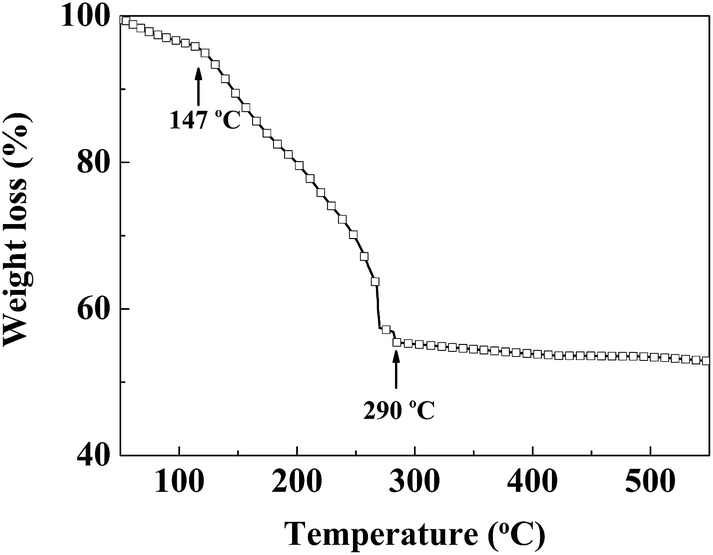 | ||
| Fig. 2 Thermogravimetric analysis of the dried In2O3 precursor solution. | ||
The XRD measurements were taken as a function of annealing temperature to clarify the crystalline state of the thin films and the results are shown in Fig. 3. The In2O3 thin films annealed at 250 and 300 °C show amorphous nature. However, when the annealing temperature was increased to 350 °C, several diffraction peaks are observed. This demonstrates that the In2O3 thin film annealed at 350 °C is crystallized. The In2O3 thin film annealed at 350 °C (JCPDS, no. 65-3170) shows (200), (222), (400), and (440) orientations located at 21.5, 30.6, 35.5, and 50.94°, respectively. The sharp peak at around 33° is attributed to the silicon substrate. This suggests that the decomposition and the densification of the In2O3 thin film occur at higher annealing temperatures, leading to a growth of the grain. It is known that the amorphous thin film has the advantage of large-area uniformity, which is crucial for commercial applications. Moreover, amorphous thin films exhibit other advantages, including smooth surface, high stability, and low interface state density.18,25
 | ||
| Fig. 3 XRD patterns of the In2O3 thin films on silicon substrates annealed at different temperatures. | ||
To better understand the formation of the In2O3 thin films, FT-IR measurements were carried out. The O–H and C–H stretching vibration shows a broad peak in the range of 3300–3700 cm−1. Peaks in the 700–1600 cm−1 range indicate O–H and NO3− deformation vibration. These bondings suppress the condensation of the metal oxide gel films by chelating with coordination bonding to the metal ions.26 The thin films also show peaks at ∼2350 cm−1, which may be due to the absorption of CO2 on the surfaces.27 As shown in Fig. 4, a large number of groups are remained in the cases of the as-spun and dried thin films. With increasing annealing temperature, the groups were gradually separated and decomposed. When the annealing temperature is higher than 350 °C, only trace amount of vibration peaks can be observed.
 | ||
| Fig. 4 FT-IR analysis of the In2O3 thin films under various annealing conditions. | ||
The chemical states of In2O3 thin films annealed at various temperatures were investigated using XPS and shown in Fig. 5. The XPS O 1s peaks are fitted, using a Gaussian method, into three peaks of 529.8, 531.3, and 532.3 eV, respectively.16,28,29 The dominant peak located at 529.8 eV is due to the lattice oxygen in a fully-coordinated environment (M–O), while the peak located at 531.3 eV is attributed to oxygen in the vicinity of an oxygen vacancy. The peak at 532.3 eV can be attributed to hydroxyl species (M–OH). With the increase of the annealing temperature, the fraction of M–O bonding is increased from 42.3% to 50.9%, whereas the fraction of oxygen vacancies and bounded hydroxyl is decreased. These results agree well with the FT-IR and XRD analysis. This indicates that more M–O bondings are formed at elevated temperatures. The evident M–OH feature at low annealing temperature also confirms the incomplete formation of the oxide lattice. The increase of In2O3 lattice will make the electron transition from valence band to conduction band easier due to the special electron configuration of 4d105s0 as an electron transport channel. The transformation from M–OH to M–O lattice will definitely affect the electrical performance of the In2O3 TFTs.30
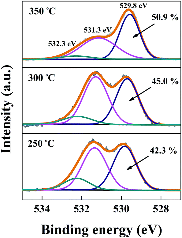 | ||
| Fig. 5 XPS O 1s analysis of the In2O3 thin films annealed at different temperatures. | ||
The surface morphologies of the In2O3 thin films annealed at various temperatures are shown in Fig. 6. The root-mean-square (RMS) roughnesses are 0.15, 0.16, and 0.19 nm for the thin films annealed at 250, 300, and 350 °C, respectively. This indicates that the solution-processed In2O3 thin films are quite smooth and uniform. Meanwhile, the grain size increases slightly with increasing annealing temperature. This can be explained as a result of few residual ligands incorporating into the lattice at higher annealing temperatures. The residual ligands suppress the growth of the grain, which is consistent with the results of XRD analysis.
 | ||
| Fig. 6 AFM morphologies of the In2O3 thin films on silicon substrates annealed at (a) 250, (b) 300, and (c) 350 °C. | ||
To evaluate the possibility of the In2O3 thin films as channel layers, the electrical performance of In2O3 TFTs based on thermally-grown SiO2 with thickness of 100 nm were investigated. All the TFT devices were integrated at the same conditions, except for the annealing temperature. The output and transfer characteristics of the In2O3 TFTs annealed at various temperatures are shown in Fig. 7. It is found that all the TFTs show n-type behaviors and work in an enhancement mode. The output curves show clear pinch-off and current saturation, the corresponding electrical parameters of the In2O3 TFTs annealed at various temperatures are summarized in Table 1.
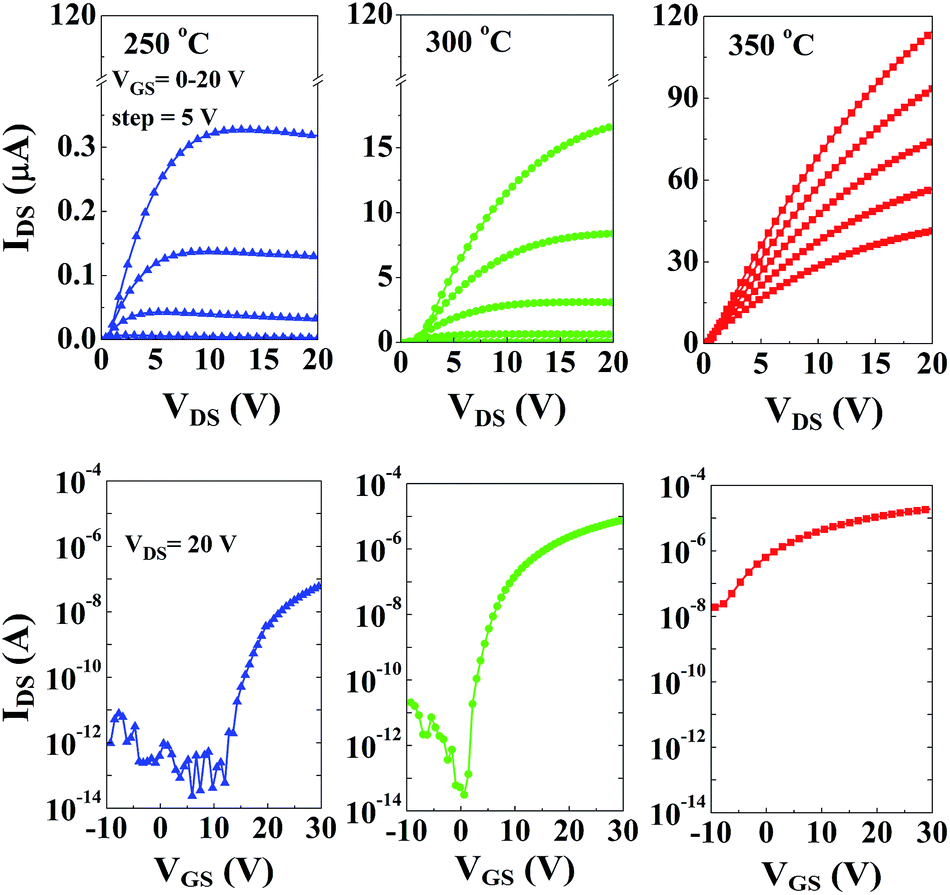 | ||
| Fig. 7 Output and transfer characteristics of In2O3 TFTs annealed at various temperatures. | ||
| Temperature (°C) | μsat (cm2 V−1 s−1) | Ion/Ioff | VTH (V) | SS (V per decade) | Dit (×1013 cm−2) | Ion (A) |
|---|---|---|---|---|---|---|
| 250 °C | 0.36 | 1.44 × 10⁶ | 20.3 | 2.51 | 1.49 | 6.44 × 10⁻⁸ |
| 300 °C | 3.08 | 1.04 × 10⁸ | 12.7 | 1.49 | 0.87 | 7.31 × 10⁻⁶ |
| 350 °C | 4.67 | 1.12 × 10³ | 3.2 | 9.04 | 5.46 | 1.93 × 10⁻⁵ |
The saturation mobility (μsat) and the threshold voltage (VTH) are calculated from the slope of IDS,sat1/2 vs. VGS according to the conventional thin film transistor model in the saturation region,31
 | (1) |
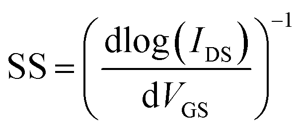
Generally, SS is directly related to the traps located in the bulk channel and/or the interface between the channel and dielectric. The subthreshold swings (SS) is given by the following equation,
 | (2) |
Consequently, trap density Dit can be estimated from SS using the equation,
 | (3) |
The number of carriers and traps has great effects on the performance of the TFT devices. As the annealing temperature was increased from 250 to 300 °C, the on-current (Ion) was increased from 6.44 × 10⁻⁸ A to 7.31 × 10⁻⁶ A, whereas the off-current (Ioff) was kept unchanged (∼5 × 10⁻¹⁴ A). When the annealing temperature was increased further (up to 350 °C), the Ion was increased from 7.31 × 10⁻⁶ A to 1.93 × 10⁻⁵ A and the Ioff was increased up to 1.73 × 10⁻⁸ A. The abrupt increase of the Ion and Ioff are due to the excess carriers flowing through the limited defects. In other words, the significant evolution of electrical performance is due to the unbalance between stoichiometry and defects. With the trade-off between carriers and traps, the In2O3 TFT annealed at 300 °C exhibits excellent device performance, which shows μsat of 3.08 cm2 V−1 s−1, Ion/Ioff of 1.04 × 10⁸, VTH of 12.7 V, and SS of 1.49 V. Therefore, we can achieve the desirable performance of the TFT by adjusting the amount of carriers and/or traps at an optimized annealing temperature.
Apart from the effect of the annealing temperature, the channel thickness also plays an important role in the electrical performance of the TFTs. The thickness dependence of the electrical performance of In2O3 TFTs was also investigated and the transfer curves are shown in Fig. 8. The Ion value was found to increase with increasing channel thickness at a fixed annealing temperature. The thicker the channel layer, the more carriers to be dragged at a same gate voltage. This will certainly result in an increase of the on-current. The electrical performances of the TFTs were thoroughly investigated.
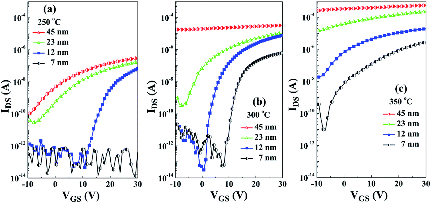 | ||
| Fig. 8 The transfer characteristics of In2O3 TFTs with various channel layer thicknesses and annealed at (a) 250 °C, (b) 300 °C, and (c) 350 °C. | ||
For clearance, the electrical performance of In2O3 TFT annealed at 300 °C with various channel thickness was calculated and summarized in Table 2. The mobility was found to be 1.24, 3.08, and 4.61 cm2 V−1 s−1 for the In2O3 TFT with the channel thickness of 7, 12, and 23 nm, respectively. Meanwhile, the In2O3 TFT exhibits ‘always-on’ state as the channel thickness is increased to 45 nm. This is mainly attributed to large number of free carriers in the channel. The Ioff was observed to be constant initially and then increased further with increasing channel thickness. Under the gate bias, the carriers were accumulated near the channel/dielectric interface. The interface defects will trap the carriers and have a further impact on the carrier transport. When the channel thickness is small, the interface defects play the most important role in prohibiting the current flow. A relatively low off current could be achieved. However, with the further increase of the channel thickness, more carriers would make contribution to the current flow, which lead to a higher off current. This is due to the limited number of the interface trap states in the thin films. To better understand the mechanism, the simplified cross-sectional views of devices with thin and thick channel layers are illustrated in Fig. 9.
| Thickness (nm) | μ (cm2 V−1 s−1) | Ion/Ioff | VTH (V) | SS (V per decade) |
|---|---|---|---|---|
| 7 | 1.24 | 1.91 × 10⁷ | 13.6 | 1.34 |
| 12 | 3.08 | 1.04 × 10⁸ | 12.7 | 1.49 |
| 23 | 4.61 | 3.32 × 10⁴ | 6.2 | 5.12 |
| 45 | Conductive | |||
 | ||
| Fig. 9 Schematic cross-section view of In2O3 TFTs with (a) thin channel and (b) thick channel. | ||
Meanwhile, we investigated the thickness dependence of the electrical performance of In2O3 TFTs annealed at 250 and 350 °C. The corresponding transfer characteristics of the TFTs are shown in Fig. 8, respectively. The same trend as the In2O3 TFTs annealed at 300 °C was observed. It is demonstrated that the channel thickness plays an important role on the electrical performance of the In2O3 TFTs.
To investigate the possibility of the improved features of the In2O3 TFT based on the high-k dielectric, ZrOx dielectric thin film was fabricated by solution process and fully solution-processed In2O3 TFT based on ZrOx was integrated. In our previous reports, we made detailed description and characterization for the ultra-thin (∼7 nm) ZrOx dielectrics.22,23,37 The ZrOx dielectric thin film exhibits a smooth surface with a roughness of 0.2 nm and pinholes free. The low leakage-current density (1 × 10⁻⁹ A cm−2 at 2.0 MV cm−1) and high breakdown electric field (7.2 MV cm−1) were observed, not only due to the smooth surface, dense structure, and high oxidation states of the ZrOx thin film, but also due to its amorphous nature. The effective dielectric constant, estimated using a series capacitor model (1/CSiO2 + 1/CZrOx = 1/Ctotal), was calculated to be around 12.5. All of the electrical properties suggest that the solution-processed ultra-thin ZrOx dielectric have great potential for fabricating the low-voltage, high-performance oxide TFTs. Fig. 10 shows the output and transfer curves of the In2O3/ZrOx TFT. The as-fabricated TFT device exhibits high performance, including a μsat of 13.01 cm2 V−1 s−1, a VTH of 1.2 V, an Ion/Ioff of 1.09 × 10⁷, and an SS of 100 mV per decade. The In2O3/ZrOx TFT shows good switching characteristics and reasonable mobility. Generally, the SS values directly correlate with the switching speed and the power consumption of the TFT devices. The small SS values for ZrOx based TFTs were beneficial from the large areal capacitance of the ZrOx dielectric and the electronic-clean interface between In2O3 and ZrOx.23,42 More importantly, it can be seen that the operating voltage is only 2 V, which is important for low-power electronic devices. It is noted that the field effect mobility of the In2O3 TFT based on ZrOx dielectric is 3 times larger than that based on SiO2 dielectric. The origin of the performance enhancement may originate from the enhanced dielectric/channel interface, smooth surface, and/or large areal capacitance of the ZrOx film.17,32,33 Presently, fully solution-processed In2O3 TFT based on high-k dielectric has seldom been investigated. Based on the results of In2O3/ZrOx TFT, we propose that solution-processed In2O3 channel layer with a high-k ZrOx dielectric is promising for fabricating low-temperature high-performance TFTs.
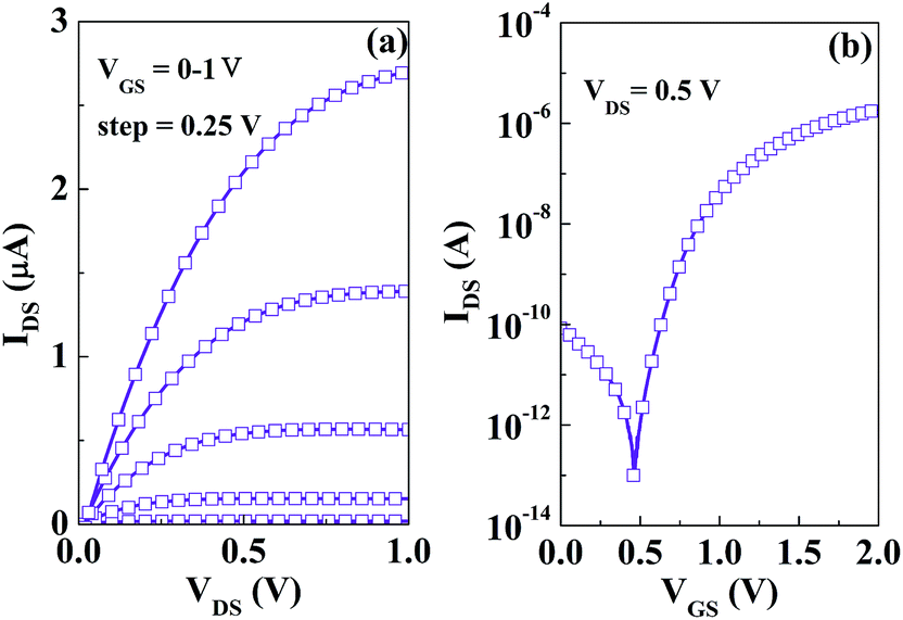 | ||
| Fig. 10 (a) Output and (b) transfer curves of solution-processed In2O3/ZrOx TFT. | ||
4. Conclusion
In summary, low-temperature high-performance solution-processed In2O3 TFTs were successfully fabricated. The annealing temperature dependence and the channel thickness dependence of the electrical performance of In2O3 TFTs were investigated. The TFT exhibits enhanced performance for 12 nm-thick In2O3 channel layer annealed at 300 °C, including a μsat of 3.08 cm2 V−1 s−1, an Ion/Ioff of 1.04 × 10⁸, a VTH of 12.7 V, and an SS of 1.49 V per decade. Finally, a fully solution-processed In2O3/ZrOx TFT was integrated, which exhibits a μsat of 13.01 cm2 V−1 s−1, a VTH of 1.2 V, an Ion/Ioff of 1.09 × 10⁷, and an SS of 100 mV per decade. It is demonstrated that solution-processed In2O3 TFTs could potentially be used for low-cost, low-temperature, and high-performance electronic devices.Acknowledgements
This study was supported by the Natural Science Foundation of China (Grant no. 51472130) and Natural Science Foundation of Shandong Province (Grant no. ZR2012FM020).References
- K. Nomura, H. Ohta, A. Takagi, T. Kamiya, M. Hirano and H. Hosono, Nature, 2004, 432, 488–492 CrossRef CAS PubMed.
- H. Yabuta, M. Sano, K. Abe, T. Aiba, T. Den, H. Kumomi, K. Nomura, T. Kamiya and H. Hosono, Appl. Phys. Lett., 2006, 89, 112123 CrossRef PubMed.
- D. H. Lee, Y. J. Chang, G. S. Herman and C. H. Chang, Adv. Mater., 2007, 19, 843–847 CrossRef CAS PubMed.
- B. Kang, W. H. Lee and K. Cho, ACS Appl. Mater. Interfaces, 2013, 5, 2302–2315 CAS.
- H. Lee, S. M. Dellatore, W. M. Miller and P. B. Messersmith, Science, 2007, 318, 426–430 CrossRef CAS PubMed.
- G. Adamopoulos, S. Thomas, P. H. wobkenberg, D. D. C. Bradley, M. A. Mclachlan and T. D. Anthopoulos, Adv. Mater., 2011, 23, 1894–1898 CrossRef CAS PubMed.
- S. Y. Han, G. S. Herman and C. Chang, J. Am. Chem. Soc., 2011, 133, 5166–5169 CrossRef CAS PubMed.
- M. G. Kim, M. G. Kanatzidis, A. Facchetti and T. J. Marks, Nat. Mater., 2011, 10, 382–388 CrossRef CAS PubMed.
- K. K. Banger, Y. Yamashita, K. Mori, R. L. Peterson, T. Leedham, J. Rickard and H. Sirringhaus, Nat. Mater., 2011, 10, 45–50 CrossRef CAS PubMed.
- Y. H. Kim, J. S. Heo, T. H. Kim, S. Park, M. H. Yoon, J. Kim, M. S. Oh, G. R. Yi, Y. Y. Noh and S. K. Park, Nature, 2012, 489, 128–133 CrossRef CAS PubMed.
- Y. H. Hwang, J. S. Seo, J. M. Yun, H. Park, S. Yang, S. H. K. Park and B. S. Bae, NPG Asia Mater., 2013, 5, e45 CrossRef CAS.
- H. S. Kim, P. D. Byrne, A. Facchetti and T. J. Marks, J. Am. Chem. Soc., 2008, 130, 12580–12581 CrossRef CAS PubMed.
- H. Y. Chong, K. W. Han, Y. S. No and T. W. Kim, Appl. Phys. Lett., 2011, 99, 161908 CrossRef PubMed.
- W. H. Jeong, G. H. Kim, H. S. Shin, B. D. Ahn, H. J. Kim, M. K. Ryu, K. B. Park, J. B. Seon and S. Y. Lee, Appl. Phys. Lett., 2010, 96, 093503 CrossRef PubMed.
- S. Jeong, J.-Y. Lee, S. S. Lee, Y. Choi and B.-H. Ryu, J. Phys. Chem. C, 2012, 115, 11773–11780 Search PubMed.
- J. S. Lee, Y. J. Kwack and W. S. Choi, ACS Appl. Mater. Interfaces, 2013, 5, 11578–11583 CAS.
- Y. M. Park, J. Daniel, M. Heeney and A. Salleo, Adv. Mater., 2011, 23, 971–974 CrossRef CAS PubMed.
- J. W. Hennek, M. G. Kim, M. G. Kanatzidis, A. Facchetti and T. J. Marks, J. Am. Chem. Soc., 2012, 134, 9593–9596 CrossRef CAS PubMed.
- C. Avis and J. Jang, J. Mater. Chem., 2011, 21, 10649–10652 RSC.
- J. Peng, Q. J. Sun, S. D. Wang, H. Q. Wang and W. L. Ma, Appl. Phys. Lett., 2013, 103, 061603 CrossRef PubMed.
- W. K. Lin, K. C. Liu, S. T. Chan and C. S. Li, Thin Solid Films, 2012, 520, 3079–3083 CrossRef CAS PubMed.
- G. X. Liu, A. Liu, F. K. Shan, Y. Meng, B. C. Shin, E. Fortunato and R. Martins, Appl. Phys. Lett., 2014, 105, 113509 CrossRef PubMed.
- A. Liu, G. X. Liu, H. H. Zhu, F. Xu, E. Fortunato, R. Martins and F. K. Shan, ACS Appl. Mater. Interfaces, 2014, 6, 17364–17369 CAS.
- J. M. Kwon, J. Jung, Y. S. Rim, D. L. Kim and H. J. Kim, ACS Appl. Mater. Interfaces, 2014, 6, 3371–3377 CAS.
- S. Aikawa, T. Nabatame and K. Tsukagoshi, Appl. Phys. Lett., 2013, 103, 172105 CrossRef PubMed.
- M. Ivanda, S. Music, S. Popovic and M. Gotic, J. Mol. Struct., 1999, 480, 645 CrossRef.
- P. R. Potti and V. C. Srivastava, Ind. Eng. Chem. Res., 2012, 51, 7948 CrossRef CAS.
- J. C. C. Fan and J. B. Goodenough, J. Appl. Phys., 1977, 48, 3524–3531 CrossRef CAS PubMed.
- Y. Jeong, K. Song, T. Jun, S. Jeong and J. Moon, Thin Solid Films, 2011, 519, 6164–6168 CrossRef CAS PubMed.
- J. S. Park, J. K. Jeong, H. J. Chung, Y. G. Mo and H. D. Kim, Appl. Phys. Lett., 2008, 92, 072104 CrossRef PubMed.
- M. G. Kim, J. W. Hennek, H. S. Kim, M. G. Kanatzidis, A. Facchetti and T. J. Marks, J. Am. Chem. Soc., 2012, 134, 11583–11593 CrossRef CAS PubMed.
- J. H. Park, Y. B. Yoo, K. H. Lee, W. S. Jang, J. Y. Oh, S. S. Chae, H. W. Lee, S. W. Han and H. K. Baik, ACS Appl. Mater. Interfaces, 2013, 5, 8067–8075 CAS.
- X. L. Xu, Q. Y. Cui, Y. Z. Jin and X. J. Guo, Appl. Phys. Lett., 2012, 101, 222114 CrossRef PubMed.
- S. Jeong, Y. G. Ha, J. Moon, A. Facchetti and T. J. Marks, Adv. Mater., 2010, 22, 1346–1350 CrossRef CAS PubMed.
- T. Kamiya, K. Nomura and H. Hosono, J. Disp. Technol., 2009, 5, 273–288 CrossRef CAS.
- H. Hosono, K. Nomura, Y. Ogo, T. Uruga and T. Kamiya, J. Non-Cryst. Solids, 2008, 354, 2796–2800 CrossRef CAS PubMed.
- G. X. Liu, A. Liu, Y. Meng, F. K. Shan, B. C. Shin, W. J. Lee and C. R. Cho, J. Nanosci. Nanotechnol., 2015, 15, 2185–2191 CrossRef CAS PubMed.
- C. H. Choi, S. Y. Han, Y. W. Su, Z. Fang, L. Y. Lin, C. C. Cheng and C. Chang, J. Mater. Chem. C, 2015, 3, 854–860 RSC.
- P. Barquinha, A. Pimentel, A. Marques, L. Pereira, R. Martins and E. Fortunato, J. Non-Cryst. Solids, 2006, 352, 1749–1752 CrossRef CAS PubMed.
- Y. Wang, X. W. Sun, G. K. L. Goh, H. V. Demir and H. Y. Yu, IEEE Trans. Electron Devices, 2011, 58, 2 CrossRef.
- D. E. Walker, M. Major, M. B. Yazdi, A. Klyszcz, M. Haeming, K. Bonrad, C. Melzer, W. Donner and H. Seggern, ACS Appl. Mater. Interfaces, 2012, 4, 6835–6841 CAS.
- G. X. Liu, A. Liu, H. H. Zhu, B. C. Shin, E. Fortunato, R. Martins, Y. Q. Wang and F. K. Shan, Adv. Funct. Mater., 2015 DOI:10.1002/adfm.201500056.
| This journal is © The Royal Society of Chemistry 2015 |