DOI:
10.1039/C5RA04133C
(Paper)
RSC Adv., 2015,
5, 44847-44852
Maskless, site-selective, nanoaerosol deposition via electro-aerodynamic jet to enhance the performance of flexible Ag-grid transparent electrodes†
Received
9th March 2015
, Accepted 12th May 2015
First published on 13th May 2015
Abstract
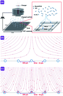
Grid-type transparent electrodes (TEs) have been fabricated using various techniques, but enhancing the performance of TEs remains challenging. In this study, we developed an aerosol deposition methodology whereby airborne silver nanoparticles of 32 nm diameter were electrically charged and delivered through a nozzle to a pre-patterned silver grid with periodic silver lines (width 18 μm, thickness 360 nm, and pitch 500 μm). A high voltage of 7 kV was applied between the nozzle and the grid, located 10 mm away from the nozzle, such that charged silver nanoparticles were deposited on the grid without the requirement for masking. The pre-patterned silver grid was prepared with AC pulse applied electrohydrodynamic jet printing on a PET film. After 3 minutes of deposition, the grid thickness increased from 360 nm to 587 nm, resulting in decreased TE sheet resistance from 7.38 Ω sq−1 to 1.95 Ω sq−1 while transmittance was kept constant at 84% (σDC/σOP ratio increased from 300 to 1050).
Introduction
Transparent electrodes (TEs) have recently received significant attention, and nanostructures may be employed to develop high-performance metal-based transparent electrodes.1–8 One model structure is a metal grid with periodic metal lines;9 this system has been investigated as a promising direction for the development of transparent electrodes, as excellent performance has been measured thus far.10 A number of researchers have fabricated metal grid TEs: Ghosh et al.11 prepared metal TEs using UV lithography; Zou et al.10 fabricated TEs using photolithography; and Jin et al.12 fabricated flexible TEs using electroless plating and photolithography. To improve the efficiency of material utilization and simplify the process steps, Jang et al.13 introduced an electrohydrodynamic (EHD) jet printing method: in this method, a strong electric field is applied to the nozzle, which leads to the elongation of the ink on the tip of the nozzle and the breakout of the ink into droplets with diameters smaller than the diameter of the nozzle. This EHD jet printing method results in fine patterning with high resolution.13–15
Optical transmittance and electrical sheet resistance are the two most significant parameters of interest for all TEs, but these are also in constant competition.9 Ideally, a TE has a low sheet resistance at high optical transmittance. Using lithography, Ghosh et al.11 and Jin et al.12 fabricated TEs with sheet resistances of 2.8 Ω sq−1 and 1.2 Ω sq−1 at 78% transmittance, respectively. EHD jet printing has also been used to fabricate TEs with a sheet resistance of 2.5 Ω sq−1 at 78% transmittance.13 The methods used in the present study13 yielded similar performance to that of lithography-made TEs11,12 but provide a simpler and more effective fabrication method for metal grid TEs.
To overcome the trade-off between optical transmittance and electrical sheet resistance, Ghosh et al.11 suggested increasing grid thickness (not width) to obtain low sheet resistance without decreasing transmittance. However, in their fabrication process, the metal grid thickness was determined by controlling the thickness of the photoresist within a mask. Therefore, it is still necessary to develop a direct writing technology in which grid thickness may be increased vertically without using a photoresist. One direct writing technology is the Aerosol Jet, a registered trademark of Optomec Inc.16,17 This technology has been used for vertical direction printing in 3-D interconnect packaging18 and for building 3-D surface structures.19 The Aerosol Jet creates particle-laden droplets and uses an aerodynamic focusing system to direct the coupled droplets and sheath air flows through a capillary nozzle where the flow is accelerated and focused. However, this droplet deposition can increase grid width during additional drying processes, and the increased grid width decreases TE transmittance. Additionally, the Aerosol Jet is more suitable for focused printing on a specific dot or line rather than parallel printing on a number of dots or lines simultaneously.
Parallel printing of nanoparticles via electrodynamic focusing of charged aerosols20,21 is another option for increasing grid thickness. Kim et al.20 used particle charging and ion injection in a parallel focusing method. Ion deposition caused charge accumulation on the photoresist surface, which distorted the initially near-flat equipotential planes into convex planes in the areas where the photoresist layer broke into patterned features. Lee et al.21 applied a parallel printing method to a 3-D assembly of nanoparticles. They structured nanoparticles in parallel and vertically, simultaneously, using holes arrayed on a photoresist. By controlling deposition time, they were able to make differently shaped structures. However, their method20,21 requires a photoresist mask for printing.
Here, we propose using an electro-aerodynamic (EAD) jet to print nanoparticles on a pre-patterned metal grid. The pre-patterned silver grid TE was prepared by using an AC-pulsed voltage for EHD jet printing, which enabled well-controlled drop-on-demand printing of Ag nanoparticles on a PET film. Printing on PET film is difficult using traditional DC-based EHD jet printing processes22 due to the residue charge on printed droplets, as discussed by Park et al.23 Details of the fabrication of silver grid TEs are presented in Park et al.24 and are briefly introduced in Methods section. The vertical thickness of the silver grid was increased through electro-aerodynamic jet printing, which is an aerosol-based printing method.25,26
Experimental section
Using an AC-pulsed voltage for EHD jet printing to prepare a flexible Ag grid TE
The setup consisted of an electrical power supply system, a moving stage system, a monitoring system, and an ink supply system. The electrical power supply system consisted of a high voltage power supply (∼AC 15 kV) used to supply a high potential between the pin-type electrode and the ground electrode. A function generator (WF1973, NF Co.) was connected to the high voltage power supply (10/40A, Trek Inc.) to generate a range of AC pulses. The frequency of the pulsed voltage was fixed at 2 kHz. The moving stage system consisted of a high-resolution linear motor type X–Y axis (JDAH100, Justek Inc., resolution: 0.1 μm, flatness: 10 μm), a digital motion controller (UMAC, Delta Tau Co.), and a vacuum chuck to hold the substrate rigidly. The stage velocity was 10 mm s−1. The monitoring system consisted of a high-speed camera (Fastcam SA1.1, Photron Inc.), an optical zoom lens, and a halogen light source (KLS-100H-RS-150, Kwangwoo Co. Ltd.); this was used to monitor the cone-jet mode and jetting status from the side view of the jetting system. A silver nanocolloid (Cabot Co.) ink was utilized (particle diameter: 30 nm) for the Ag grid fabrication process. A cone-shaped glass capillary nozzle (base diameter: 1.5 mm, tip diameter: 50 μm) was mounted in a capillary holder where an ink inlet port was located. To supply high voltage to the ink, a pin-type stainless electrode (diameter: 0.3 mm) was inserted into the base side of the glass capillary nozzle. A syringe pump (KDS200, KD Scientific Inc.) controlled flow rates with varying syringe infusion speeds (minimum flow rate = 1.38 nl min−1, maximum flow rate = 2119 μl min−1 for a 1 ml syringe). During the printing process, the copper ground electrode was located 200 μm below the nozzle. Under fixed flow rate conditions (0.1 μl min−1), each positive or negative pulse produced a jet when an AC voltage of 1.4 kV (peak-to-peak) and 2 kHz (pulse frequency) was applied. A PET film (Freemteck, Korea) was used as the substrate, which was located on the ground electrode. After Ag grid patterning, TEs (30 mm × 30 mm) were placed on a hotplate for a sintering process at a temperature of 180 °C for 20 min. Details of experimental setup is shown in Fig. S-1 of the ESI.†
EAD jet printing to increase of TE metal grid thickness
The set-up consisted of aerosolization, charging, and deposition of silver nanoparticles. After compressed air was passed through a clean air supply consisting of an oil trap, a diffusion dryer, and a high efficiency particulate air (HEPA) filter, the particle-free compressed air entered a Collison type atomizer (9302, TSI Inc., USA), which was filled with silver nanoparticle (diameter 30 nm) solution. Dry clean air at 2 lpm formed a high-velocity jet through an orifice in the atomizer. The pressure drop from this jet drew the solution up through a tube. The solution was then broken into droplets by the high-velocity air jet. The resultant larger droplets impinged on an impactor, while the smaller droplets made no contact and formed an aerosol that exited through an outlet. The aerosol flow rate was controlled by a rotameter. The aerosolized silver nanoparticles were passed through a diffusion dryer for water removal and a neutralizer (Soft X-ray charger 4530, HCT, Korea) to induce a Boltzmann charge distribution. The neutralized silver nanoparticles entered a unipolar charger where a stainless steel needle (wire) electrode, located at the center, was used to generate corona discharge on its sharp tip. The corona discharge generated air ions, which moved along the electric field to a grounded cylinder (made of duralumin). The amount of charge per particle was controlled by a DC voltage supplied from a high voltage power supply. A voltage of −8 kV was applied to the needle to charge the particles. Charged silver nanoparticles (average charge of 3.2) were focused on the silver grid under the influence of the electro-aerodynamic force between the nozzle and conductive grid. A voltage of 7 kV was applied between the nozzle and the grid. With a nozzle diameter of 6 mm and a distance between nozzle and substrate of 10 mm, the deposition area was 14 mm × 14 mm. Schematic details of EAD jet printing are shown in Fig. S-2 of the ESI.†
Results and discussions
In the EAD jet printing method, aerosolized and dried particles are unipolar charged when they pass through a corona charger, and move toward the metal grid after they pass through a nozzle, as shown in Fig. 1(a). Because an external electric field is applied between the nozzle and the metal grid, particles rarely deposit on the space between metal lines: they are forced to deposit on the metal lines. For one stationary position configuration of the nozzle and substrate, the deposition area covered approximately 14 mm × 14 mm when the nozzle diameter was 6 mm, and the distance between the nozzle and the substrate was 10 mm. Fig. 1(b) and (c) show the effects of the electric field on particle deposition. When no voltage was applied, as shown in Fig. 1(b), no particles were deposited either on the metal grids or the space between the grids. Even though particles were charged, they escaped in the direction of the flow. In contrast, Fig. 1(c) shows that with an applied electric field of 7 kV per 10 mm, all particles were deposited on the grids but not on the spaces between. Analyses were conducted using FLUENT, a commercial computational fluid dynamics (CFD) software, with an external user defined function (UDF) code (details are presented in the ESI†).
 |
| Fig. 1 Site-selective, mask-less nanoparticle deposition through EAD jet printing to increase the thickness of a metal grid. (a) Particle patterning via EAD jet printing. (b) Particle trajectory without an electric field. (c) Particle trajectory with an electric field. | |
Fig. 2 shows the morphologies of silver grids obtained with varying EAD printing times. Printed silver nanoparticles were treated at a temperature of 180 °C. Regions 1 and 2 refer to part of a metal line and a space between metal lines, respectively. For the control condition (no EAD printing), Fig. 2(a) shows field emission scanning electron microscopy (FE-SEM) images of the flexible transparent metal grid prepared by EHD jet printing with a line width of 18 μm and a line pitch of 500 μm, resulting in a filling factor (FF) of 0.07. As expected, nanoparticles were densely and uniformly deposited in region 1, and no nanoparticles were deposited in region 2. With increasing EAD printing time, Fig. 2(b)–(d) show that vertical nanoparticle deposition on the prepared silver grid also increased. For the EAD jet printing process, aerosolized and dried silver nanoparticles (30 nm in diameter) were charged via a corona charger. Charged nanoparticles (average charge of 3.2)27 were focused on the Ag grid under the influence of an electro-aerodynamic force (flow rate of 2 lpm and applied voltage of 7 kV between the nozzle and the grid). Interestingly, no particles were deposited in region 2 for all the EAD printing times.
 |
| Fig. 2 SEM images of the changing morphology of an Ag grid with EAD jet printing of Ag nanoparticles. (a) Ag grid after EHD printing (before EAD). (b)–(d) Ag grids with varying EAD jet printing time. | |
Fig. 3 shows atomic force microscopy (AFM) images of the prepared Ag grid flexible transparent electrode, before and after EAD jet printing. Fig. 3(a) shows that the Ag grid prepared using EHD jet printing had a thickness of 360 nm. Fig. 3(b)–(d) clearly show that the Ag grid grew in the vertical direction with no width variation. Grid thickness increased linearly with EAD jet printing time. With a deposition time of 3 min, grid thickness increased by 227 nm (around 76 nm min−1).
 |
| Fig. 3 (a)–(d) AFM images of Ag grid. (e) Comparison between calculations and experiments. | |
Experimental results were also compared with calculated parameters using the following equation:
|
 | (1) |
where Δ
H is the thickness increase using EAD printing,
Ntotal is the total number concentration of particles obtained using a scanning mobility particle sizer (SMPS) system consisting of a differential mobility analyzer (DMA, 3081, TSI, USA) and a condensation particle counter (CPC, 3025, TSI, USA),
Q is the flow rate (2 lpm),
V is the particle volume (details of particle size measurement are shown in ESI
†),
A is the TE area (14 × 14 mm
2), FF is the filling factor (0.07), and
t is the EAD printing time. Based on calculations, the grid thickness using EAD jet printing was expected to increase by 80 nm min
−1, which was in good agreement with the experimental results, as shown in
Fig. 3(e).
Optical transmittance spectra (measured with an IV-visible spectrophotometer, Luvra, S12, Biochrom) in the visible region and sheet resistances (measured with a four-point probe, FPP-400, Dasol Eng) were obtained and are shown in Fig. 4. Fig. 4(a) shows that optical transmittance was about 90% for the bare PET film, but this decreased slightly with nanoparticle printing. One interesting observation was that optical transmittance was around 84% for all printing cases. The sheet resistance was 7.38 Ω sq−1 for the sample prepared using EHD printing but decreased to 4.01 Ω sq−1, 2.64 Ω sq−1, and 1.95 Ω sq−1 after additional EAD printing for 1 min, 2 min, and 3 min, respectively. To evaluate the durability of flexible Ag grid TEs under stress, the sheet resistances of Ag grid electrodes were measured at a bending radius of 2 mm. Fig. 4(b) presents the results: the sheet resistances of the Ag grid electrode increased very slightly, less than 25% from the original value, even after 500 cycles, indicating the high durability of flexible Ag grid electrodes.
 |
| Fig. 4 Images of fabricated flexible transparent electrodes and plots of optical transmittance spectra and sheet resistance with bending cycle. (a) Optical transmittance spectra. (b) Sheet resistance as a function of bending cycle (∼500 times). | |
Fig. 5 shows the optical transmittances of Ag grid TEs plotted against sheet resistance and compares these with the results of previous research. The performance of a transparent, conductive thin film can be evaluated using the relationship suggested by Dressel and Gruner:28
|
 | (2) |
where
σOP(
λ) is the optical conductivity and
σDC is the DC conductivity of the transparent electrode. With regard to metal grid TEs investigated in previous studies
10–13 (see
Fig. 5), Zou
et al.10 and Jang
et al.13 reported
σDC/
σOP ratios of almost 200 and 70, respectively, while Ghosh
et al.11 reported ratios ranging from 10–70. Most
σDC/
σOP values range between two solid lines, representing
σDC/
σOP ratios of 10 and 300. However, Jin
et al.12 achieved a
σDC/
σOP ratio of 1000 at 77% transmittance, and a
σDC/
σOP ratio of 550 at 88% transmittance. The ratios for TEs fabricated in our study matched the curves for
σDC/
σOP = 300, 550, 800, and 1050 for EHD jet printing, and 1, 2, and 3 min of additional EAD jet printing, respectively. EAD jet printing had a significant effect on enhancing the
σDC/
σOP ratio: the curve was shifted to the left while maintaining a transmittance of 84%.
 |
| Fig. 5 Plot of transmittance (at 550 nm) as a function of sheet resistance. | |
Conclusions
In summary, we developed a new methodology for enhancing the σDC/σOP ratio of flexible metal-grid TEs without decreasing optical transmittance. We used EAD jet printing, which is a mask-less, site-selective nanoparticle deposition technology, as well as EHD jet printing. A pre-patterned silver grid (width 18 μm, thickness 360 nm, pitch 500 μm) was prepared using an AC-pulsed voltage for EHD jet printing on a PET film. After 3 minutes of EAD with silver nanoparticles, grid thickness increased from 360 nm to 587 nm, resulting in decreasing TE sheet resistance, from 7.38 Ω sq−1 to 1.95 Ω sq−1, while transmittance was kept constant at 84% (σDC/σOP ratio increased from 300 to 1050). This technique extends the capability of EAD jet printing on various devices, and could serve as a foundation for future optical, magnetic, and electronic devices in multiple dimensions.
Acknowledgements
This work was supported by the BioNano Health-Guard Research Center funded by the Ministry of Science, ICT & Future Planning (MSIP) of Korea as Global Frontier Project (Grant Number H-GUARD_2013M3A6B2078959).
References
- P. B. Catrysse and S. Fan, Nano Lett., 2010, 10, 2944–2949 CrossRef CAS PubMed
. - J. Van de Groep, P. Spinelli and A. Polman, Nano Lett., 2012, 12, 3138–3144 CrossRef CAS PubMed
. - H. Wu, L. Hu, M. W. Rowell, D. Kong, J. J. Cha, J. R. McDonough, J. Zhu, Y. Yang, M. D. McGehee and Y. Cui, Nano Lett., 2010, 10, 4242–4248 CrossRef CAS PubMed
. - M. Layani and S. Magdassi, J. Mater. Chem., 2011, 21, 15378–15382 RSC
. - S. Ye, A. R. Rathmell, Z. Chen, I. E. Stewart and B. J. Wiley, Adv. Mater., 2014, 26, 6670–6687 CrossRef CAS PubMed
. - K. Higashitani, C. E. McNamee and M. Nakayama, Langmuir, 2011, 27, 2080–2083 CrossRef CAS PubMed
. - S. E. Park, S. Kim, D. Y. Lee, E. Kim and J. Hwang, J. Mater. Chem. A, 2013, 1, 14286–14293 CAS
. - T. Tokuno, M. Nogi, M. Karakawa, J. Jiu, T. T. Nge, Y. Aso and K. Suganuma, Nano Res., 2011, 4, 1215–1222 CrossRef CAS
. - L. Hu, H. Wu and Y. Cui, MRS Bull., 2011, 36, 760–765 CrossRef CAS
. - J. Zou, H. L. Yip, S. K. Hau and A. K. Y. Jen, Appl. Phys. Lett., 2010, 96, 203301 CrossRef PubMed
. - D. S. Ghosh, T. L. Chen and V. Pruneri, Appl. Phys. Lett., 2010, 96, 041109 CrossRef PubMed
. - Y. Jin, Y. Cheng, D. Deng, C. Jiang, T. Qi, D. Yang and F. Xiao, ACS App. Mater. Interfaces, 2014, 6, 1447–1453 CrossRef CAS PubMed
. - Y. Jang, J. Kim and D. Byun, J. Phys. D: Appl. Phys., 2013, 46, 155103 CrossRef
. - V. D. Nguyen, M. G. Schrlau, S. B. Tran, H. H. Bau, H. S. Ko and D. Byun, J. Nanosci. Nanotechnol., 2009, 9, 7298 CAS
. - V. D. Nguyen and D. Byun, Appl. Phys. Lett., 2009, 9, 7298 CAS
. - M. Mette, Prog. Photovoltaics, 2007, 15, 621–627 Search PubMed
. - A. M. Sukeshini, F. Meisenkothen, P. Gardner and T. L. Reitz, J. Power Sources, 2013, 224, 295–303 CrossRef PubMed
. - S. Stoukatch, P. Laurent, S. Dricot, F. Axisa, L. Seronveaux, D. Vandormael, E. Beeckman, B. Heusdens and J. Destine, IEEE Electronic system-integration technology conference, 4th, 2012, pp. 1–5 Search PubMed
. - M. Hedges and A. B. Marin, IEEE polymers and adhesives in microelectronics and photonics conference, 5th, 2005, pp. 53–57 Search PubMed
. - H. Kim, J. Kim, H. Yang, J. Suh, T. Kim, B. Han, S. Kim, D. S. Kim, P. V. Pikhitsa and M. Choi, Nat. Nanotechnol., 2006, 1, 117–121 CrossRef CAS PubMed
. - H. Lee, S. You, P. V. Pikhitsa, J. Kim, S. Kwon, C. G. Woo and M. Choi, Nano Lett., 2011, 11, 119–124 CrossRef CAS PubMed
. - C. Wei, H. Qin, N. A. Ramirez-Iglesias, C. P. Chiu, Y. S. Lee and J. Dong, J. Micromech. Microeng., 2014, 24, 045010 CrossRef
. - J. U. Park, M. Hardy, S. J. Kang, K. Barton, K. Adair, D. K. Mukhopadhyay, C. Y. Lee, M. S. Strano, A. G. Alleyne, J. G. Georgiadis, P. M. Ferreira and J. A. Rogers, Nat. Mater., 2007, 6, 728–789 Search PubMed
. - J. Park and J. Hwang, J. Phys. D: Appl. Phys., 2014, 47, 405102 CrossRef
. - J. Park, J. Jeong, C. Kim and J. Hwang, Aerosol Sci. Technol., 2013, 47, 512–519 CrossRef CAS PubMed
. - K. T. Park and J. Hwang, Carbon, 2014, 75, 401–410 CrossRef CAS PubMed
. - J. Park, C. Kim, J. Jeong, S. G. Lee and J. Hwang, J. Electrost., 2011, 69, 126–132 CrossRef PubMed
. - M. G. Dressel and G. Gruner, Electrodynamics of solids: Optical properties of electrons in matter, Cambridge University Press, Cambridge, 2002 Search PubMed
.
Footnote |
† Electronic supplementary information (ESI) available: Details of using an AC-pulsed voltage for EHD jet printing to fabricate flexible Ag grid TEs, using EAD jet printing to control TE metal grid, a numerical study of EAD jet printing, and size distribution measurement of silver aerosols. See DOI: 10.1039/c5ra04133c |
|
This journal is © The Royal Society of Chemistry 2015 |
Click here to see how this site uses Cookies. View our privacy policy here.