
Homostructured negative differential resistance device based on zigzag phosphorene nanoribbons
Chenhui Zhang ab,
Gang Xiang*ab,
Mu Lanab,
Zhijie Tangab,
Lidong Dengab and
Xi Zhang*ab
ab,
Gang Xiang*ab,
Mu Lanab,
Zhijie Tangab,
Lidong Dengab and
Xi Zhang*ab
aCollege of Physical Science and Technology, Sichuan University, Chengdu 610064, China. E-mail: gxiang@scu.edu.cn; xizhang@scu.edu.cn
bKey Laboratory of High Energy Density Physics and Technology of Ministry of Education, Sichuan University, Chengdu 610064, China
First published on 9th April 2015
Abstract
The electronic transport properties of zigzag phosphorene nanoribbon (ZPNR) homostructures are investigated using density functional theory calculations and the nonequilibrium Green’s function technique. The proposed devices have simple constructions but exhibit robust negative differential resistance (NDR) as well as quite large current, which implies great potential for building nanoelectronic devices. Through the analysis of the electronic structures and transmission spectra, we give a clear physical picture of the NDR mechanism, in which such current–voltage (I–V) behaviors originate from the bias-dependent interaction between the discrete density of states (DOS) peaks of the electrodes and the narrow states around the Fermi level in the scattering region.
1. Introduction
Over the past several years, there has been extraordinary enthusiasm injected into the frontier area of two-dimensional (2D) crystal materials with atomic thickness.1–5 Among the numerous candidates, graphene and molybdenum disulfide (MoS2) are two bright stars.6–8 Owing to the massless Dirac feature, graphene shows ultra-high charge carrier mobility.6 But unfortunately, the absence of a band gap becomes its Achilles’ heel. Monolayer MoS2 possesses the benefit of a direct band gap of ∼1.8 eV,8 however, the fabricated transistors perform with a relatively deficient mobility of a few hundred square centimeters per volt per second.9Very recently, a new 2D material named phosphorene was successfully exfoliated from bulk black phosphorus and immediately attracted great attention.10–16 A carrier mobility up to ∼1000 cm2 (V s)−1 and a high on–off ratio of 105 were measured in few-layer phosphorene field-effect transistors.10 This novel material has a direct band gap, tunable from 1.51 eV for a monolayer to 0.59 eV for a five-layer sample.12 Unlike other currently studied 2D materials, phosphorene shows a strong in-plane anisotropic nature, including band structure, mechanical properties, electrical conductivity, thermal conductivity, and optoelectronic responses,12–17 which endow it with inimitable glamour. So it is reasonable to convert a 2D phosphorene sheet to 1D nanoribbons for electronic modulation, and many interesting results have been reported.18–21 The unexpected merging of nonrelativistic and relativistic carrier behaviors in a single material may endue phosphorene nanoribbons (PNRs) with novel transport properties.18 Based on these facts, we are very interested in the I–V characteristics of PNRs. Considering that the pristine ZPNRs are metals regardless of the ribbon width,19–21 they can be used as a scattering region as well as electrodes directly without any connection problem, which is desirable for applications.
NDR is a property of some electrical devices in which an increase of bias voltage results in a decrease in current. In 1958, Leo Esaki discovered NDR phenomena in heavily doped Ge p–n junctions22 and proposed the tunnel diode. Afterwards, the resonant tunneling diode (RTD)23 was invented and widely applied in electrical circuits. Until now, a variety of material systems, including conductive polymers,24 atomic wires,25 and organic molecules,26,27 have been discovered which possess NDR character. Besides, researchers have made great efforts to explore the NDR mechanisms, such as the rotational symmetry selection rule,28 the current-driven charge transfer and conformational change,29 the asymmetric couplings between both contacts,30 and the half-filled energy bands.31 In this work, we reveal for the first time nonlinear I–V behaviors and robust NDR in a homostructured device based on ZPNRs. The analysis of the calculated electronic structures and transmission spectra give an insight into the observed results. Our original discoveries imply that ZPNRs hold great potential for electronic applications, e.g., dynatron oscillators, high-speed switches, multi-valued memories and logic devices.32
2. Calculation methods
The unpassivated edge monolayer ZPNR investigated in this work is illustrated in Fig. 1. The device with a two-probe system is divided into three parts: semi-infinite left and right electrodes are bridged by a confined central scattering region. The primitive unit cell, in which the lattice constant c0, of both electrodes and the scattering region are the same and is marked by dashed lines in Fig. 1. The length of the central region in the represented system is 5c0, and the numbers listed at the left side indicate the width of the ZPNR, thus such a device is called D54 for simplification. We performed a comprehensive first-principles study of the transport characteristics of ZPNRs with different ribbon widths from 3 to 6. The edges of D54 were then terminated by O or H atoms (i.e. DO54 and DH54, respectively) for further investigations. | ||
| Fig. 1 Schematic illustration of the proposed ZPNR based device. The green rectangles denote the left and right electrodes (they are all semi-infinite in the simulation process), and the scattering region is between them. The dashed rectangle is presented as one unit cell with the lattice constant c0. The numbers listed at left side indicate the width of the ZPNR. Blue balls denote phosphorus atoms. | ||
Geometry relaxations and electronic structures are calculated using self-consistent density functional theory as implemented in the SIESTA package,33 which uses a linear combination of atomic orbitals (LCAO) as a basis set and Troullier–Martin type34 nonlocal pseudo-potential. The exchange–correlation functional of the generalized gradient approximation (GGA) was represented by the Perdew–Burke–Ernzerh of approximation (PBE).35 The energy cutoff for the plane waves was 500 Ry and the Brillouin zone was sampled using a 1 × 1 × 50 Monkhorst–Pack grid. The initial structures were fully optimized until the Hellmann–Feynman forces tolerance reached 0.01 eV Å−1. Periodic boundary conditions, vacuum spaces of at least 15 Å, were imposed on the plane perpendicular to the Z axis of the ribbon.
The electronic transport properties were studied by the non-equilibrium Green’s function technique as implemented in the TranSIESTA package.36 A single-ζ polarized basis set was used. Test calculations with larger basis set were performed, which gave qualitatively the same results. The I–V curves were calculated with the Landauer–Buttiker formula,37
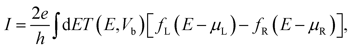 | (1) |
| eVb = μL − μR. | (2) |
3. Results and discussion
The metallic character of pristine ZPNRs with width W = 4 is evident from the computed band structures and total density of states (DOS) as shown in Fig. 2(a) and (b), verifying that such nanomaterials can be used as good conducting electrodes. The partial charge density distribution corresponding to the energy interval near the Fermi level is also plotted (Fig. 2(c)). We found that the conductivity of the system is dominated by the P atoms near the edges of the ZPNRs, as conductivity is closely related to charge density around the Fermi level. Another very striking feature is that there are several discrete DOS peaks crossing the Fermi level. Afterwards, we saw that the on-and-off alignment of the discrete DOS peaks of the two electrodes and the channel states in the scattering region results in the NDR behavior. | ||
| Fig. 2 (a) Band structures and (b) DOS of unpassivated edge ZPNRs with width W = 4. (c) Isosurfaces of the charge densities of bands corresponding to the energy interval from the Fermi level to 0.1 eV above it. The pink isosurfaces represent a charge of 0.002 e Å−3. | ||
Then we examined the I–V characteristics through the devices. In Fig. 3(a), all the pristine ZPNRs exhibit robust NDR phenomena, in which current decreases with the increase of voltage in some bias windows. In the D54 system, the current increases with the applied bias voltage and reaches the maximum value of 37.6 μA at Vb = 0.3 V. When Vb continuously increases, however, the current decreases dramatically, and consequently the NDR phenomenon arises. The first current valley occurs at Vb = 0.8 V, and afterwards there follows an undulating curve at higher voltage values. The peak current, appearing at Vb = 0.3 V, is width-dependent, and it ascends with the ribbon width as shown in Fig. 3(a). Subsequently, the edges of the D54 system were terminated by O and H atoms, respectively. As readily seen in Fig. 3(c) and (e), DO54 remains metallic while DH54 shows semiconductor behavior, which is fully consistent with a previous investigation of edge effects on the electronic properties of PNRs.20 Interestingly, we also observed a robust NDR effect in the DO54 system, shown in Fig. 3(b), and the peak current value is almost twice of that in D54. The minimum current value of 37.2 μA is obtained at Vb = 1.0 V. However, the I–V curve of DH54 is quite different. In Fig. 3(d), there is no carrier hopping between the electrodes and the scattering region when the bias range is limited below 1.4 V. Nevertheless, we see a monotonic current response to a voltage of Vb > 1.4 V. Note that DH54 is a direct band gap material having ∼1.4 eV gap value (see Fig. 3(e)), applying a bias voltage shifts the Fermi level of the left and right electrodes up and down, respectively. So the current starts flowing once the top of the valence band of the left electrode matches in energy with the bottom of the conduction band of the right electrode at bias voltage value of 1.4 V. No NDR phenomena was observed in a wide bias voltage range in DH54.
 | ||
| Fig. 3 (a) I–V curves of unpassivated edge ZPNRs-based devices with ribbon widths from 3 to 6. (b) I–V curves of D54 and DO54. (c) Band structures of O-saturated ZPNRs with width W = 4. (d) I–V curve of DH54. (e) Band structures of H-saturated ZPNRs with width W = 4. | ||
To clarify the NDR phenomenon, we turned to check the bias-dependent transmission spectrum, belonging to D54 which is illustrated in Fig. 4(a) for example. Fig. 4(b) is the color contour map, and the purple dashed lines label the integral energy interval under the applied bias. We can see clearly that there is a broad transmission hathpace crossing the Fermi level at low bias voltage, resulting in good transport at the beginning. When the bias continuously increases, the transmission hathpace becomes narrower and vanishes at last. Thus the current decreases and never exceeds the peak value of 37.6 μA obtained at 0.3 V, in spite of the subsequent appearance of a relatively small transmission peak between points C and E in Fig. 3(b). The NDR phenomenon occurs.
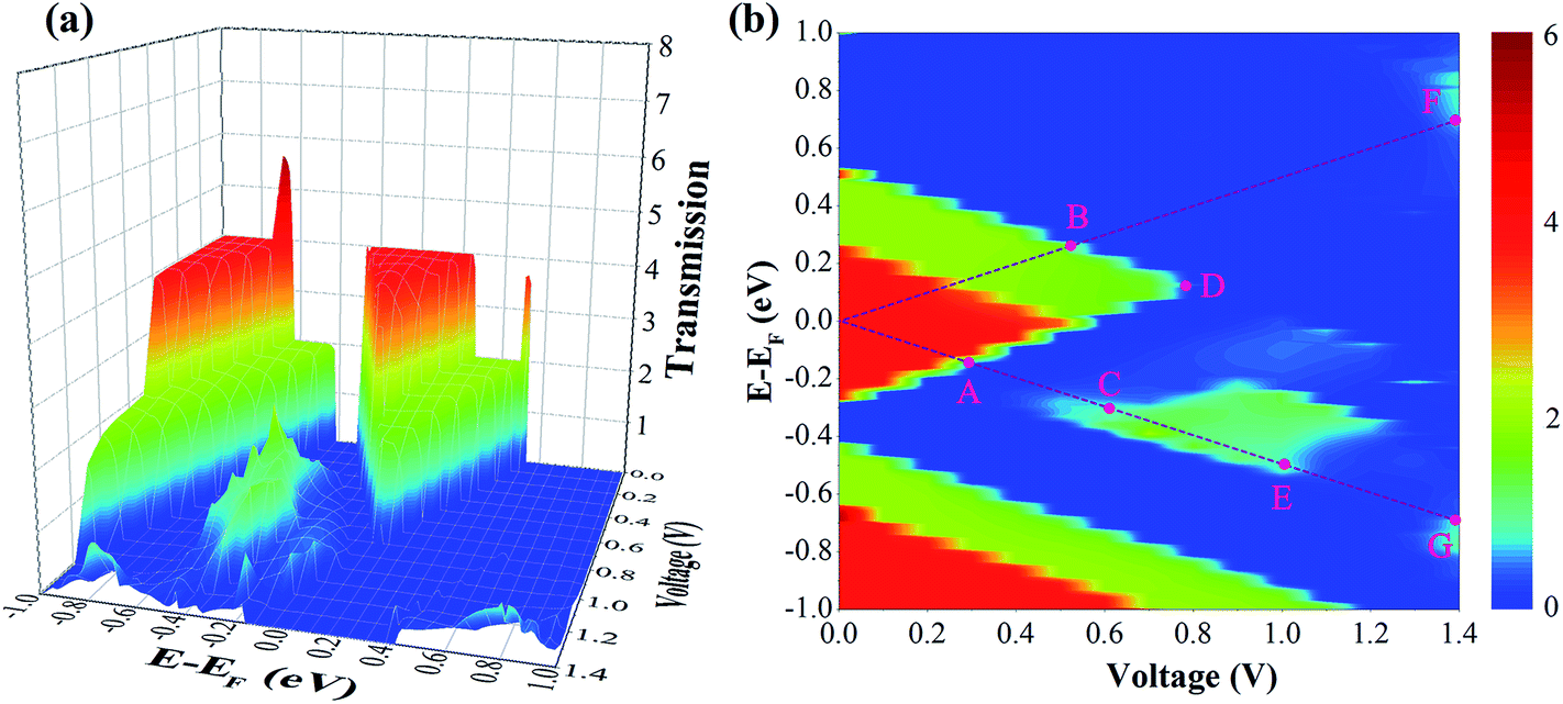 | ||
| Fig. 4 The bias-dependent transmission spectrum of D54: (a) 3D-view; (b) color contour map, and the purple dashed lines label the integral energy interval under the applied bias. | ||
The projected DOS (PDOS) of the scattering region in the D54 device is represented in Fig. 5(a), in which there are two narrow sharp peaks labelled as α and β lying at ∼±0.25 eV, corresponding to the lowest unoccupied molecular orbital (LUMO) and highest occupied molecular orbital (HOMO) of the scattering region, respectively. Subsequently, we plot a schematic model of the D54 system under different bias voltages in Fig. 5(b)–(f) in order to explore the mechanism of the NDR character. The purple and blue rectangles represent the conduction and valence bands of the two electrodes respectively corresponding to discrete DOS peak distribution around the Fermi level in Fig. 2(b). Two red lines, which act as two tunneling channels, between the electrodes in Fig. 5(b)–(f) indicate the positions of the LUMO and HOMO of the scattering region. We assumed that the two tunneling channels did not obviously change with the applied bias voltage for simplicity. For the device with zero-bias voltage, the HOMO and LUMO of the scattering region match well with the valence and conduction bands of the two electrodes (see Fig. 5(b)). So, in the resonant tunneling regime, there is a significant and broad transmission hathpace crossing the Fermi level in Fig. 4(a), and the current through the scattering region increased at the beginning. When a bias voltage of 0.3 V was applied, the Fermi levels of the left and right electrodes were shifted upwards and downwards by 0.15 V, respectively. Consequently, the HOMO of the scattering region just caught the bottom of the uppermost valence band of the left electrode (Fig. 5(c)), corresponding to point A in Fig. 4(b). Thus the carrier hopping between the left electrode and the scattering region became inhibited and the NDR arose. In a similar manner, point B in Fig. 4(b) results from the LUMO of the scattering region catching the edge of the lowermost conduction band of the right electrode (Vb = 0.5 V). When the bias increased to 0.6 V, the HOMO was located at the top of the second valence band of the left electrode (Fig. 5(d)), which can be verified in Fig. 4(b) where a small transmission peak enters into the integral energy range at point C. This is helpful for transport. But on the other side, we should consider the fact that the main transmission hathpace around the Fermi level still shrunk. So the current kept on decreasing but a little gentler from 0.6 to 0.8 V, which can be confirmed by the I–V curve of D54 plotted in Fig. 3(a) and (b). When the main transmission hathpace vanished at Vb = 0.8 V (point D in Fig. 4(b)), the NDR ended and the current increased again. It is easy to understand that the current peak at 1.0 V is due to the subsequent mismatching of the HOMO and the second valence band of the left electrode (Fig. 5(e)), corresponding to point E in Fig. 4(b). However, the carrier hopping became good again when the bias increased to 1.4 V. The transmission peaks at points F and G in Fig. 4(b) are due to the LUMO and HOMO catching the second conduction band of the right electrode and the third valence band of the left electrode in Fig. 5(f), respectively.
 | ||
| Fig. 5 (a) The PDOS of the scattering region in the D54 device. α and β refer to the two narrow sharp peaks lying at ∼±0.25 eV. (b)–(f) Schematic illustrations of the positions of the HOMO and LUMO states (the two red lines) in the scattering region relative to the discrete bands in the two electrodes with bias voltages of 0.0 V, 0.3 V, 0.6 V, 1.0 V, and 1.4 V, respectively. The conduction and valence bands of the two electrodes are represented by purple and blue rectangles respectively for simplification. | ||
The above analysis reveals an accordant corresponding relationship between transport properties and bias-dependent band distribution of the two electrodes, which give us a clear understanding of the NDR mechanism. The I–V characteristics are sample-dependent, since, undoubtedly, the electronic structures of the proposed devices are personalized. For instance, the individual differences of the DOS gap widths will certainly result in the inequality of the NDR duration. In our work, there is no need for an additional modification process, like electrode doping,31,38,39 inducing defects,40 applying strain41 or other special functionalization,42 to obtain robust NDR. Through edge O-passivation, the peak current value is greatly enhanced and considerably larger than previous reports,31,38–40,42–44 which can result in short charging time on digital circuits and high output power in RF applications. Also we don’t have the problem of distinguishing which part is mainly responsible for NDR since the electrodes and scattering region are made of the same material.45
4. Conclusions
In summary, the I–V characteristics of homostructured ZPNRs with different ribbon widths and edge passivation were examined by using first-principles calculations, most of which exhibited robust NDR behaviors. Through the analysis of the calculated electronic structures and transmission spectra, we gave a clear physical picture of the NDR mechanism, such I–V behavior originated from the bias-dependent interaction between the discrete DOS peaks of the electrodes and the channel states in the scattering region. The ZPNRs were cut from monolayer phosphorene directly without the need for other modification processes. Additionally, we suppose that the scattering region used in our work can be replaced by various molecules to fabricate novel NDR junctions.43,44 Thus our original discoveries imply that ZPNRs hold great potentials for NDR-based nanoelectronic applications.Acknowledgements
This work is supported by the National Natural Science Foundation of China (Grant no.11174212), the Program for New Century Excellent Talents in University of the Ministry of Education of China (Grant no. 11-0351), and the Scientific Research Staring Foundation for the Returned Overseas Chinese Scholars, Ministry of Education of China.References
- K. S. Novoselov, D. Jiang, F. Schedin, T. J. Booth, V. V. Khotkevich, S. V. Morozov and A. K. Geim, Proc. Natl. Acad. Sci. U. S. A., 2005, 102, 10451–10453 CrossRef CAS PubMed.
- C. H. Jin, F. Lin, K. Suenaga and S. Iijima, Phys. Rev. Lett., 2009, 102, 195505 CrossRef.
- P. Vogt, P. De Padova, C. Quaresima, J. Avila, E. Frantzeskakis, M. C. Asensio, A. Resta, B. Ealet and G. Le Lay, Phys. Rev. Lett., 2012, 108, 155501 CrossRef.
- M. Chhowalla, H. S. Shin, G. Eda, L.-J. Li, K. P. Loh and H. Zhang, Nat. Chem., 2013, 5, 263–275 CrossRef PubMed.
- A. C. Ferrari, F. Bonaccorso, V. Falko, K. S. Novoselov, S. Roche, P. Bøggild, S. Borini, F. Koppens, V. Palermo and N. Pugno, Nanoscale, 2014, 7, 4598–4810 RSC.
- K. S. Novoselov, A. K. Geim, S. V. Morozov, D. Jiang, M. I. Katsnelson, I. V. Grigorieva, S. V. Dubonos and A. A. Firsov, Nature, 2005, 438, 197–200 CrossRef CAS PubMed.
- A. K. Geim and K. S. Novoselov, Nat. Mater., 2007, 6, 183–191 CrossRef CAS PubMed.
- K. F. Mak, C. Lee, J. Hone, J. Shan and T. F. Heinz, Phys. Rev. Lett., 2010, 105, 136805 CrossRef.
- B. Radisavljevic, A. Radenovic, J. Brivio, V. Giacometti and A. Kis, Nat. Nanotechnol., 2011, 6, 147–150 CrossRef CAS PubMed.
- L. K. Li, Y. J. Yu, G. J. Ye, Q. Q. Ge, X. D. Ou, H. Wu, D. L. Feng, X. H. Chen and Y. B. Zhang, Nat. Nanotechnol., 2014, 9, 372–377 CrossRef CAS PubMed.
- H. Liu, A. T. Neal, Z. Zhu, Z. Luo, X. F. Xu, D. Tománek and P. D. Ye, ACS Nano, 2014, 8, 4033–4041 CrossRef CAS PubMed.
- J. S. Qiao, X. H. Kong, Z.-X. Hu, F. Yang and W. Ji, Nat. Commun., 2014, 5, 4475 CAS.
- R. X. Fei, A. Faghaninia, R. Soklaski, J.-A. Yan, C. Lo and L. Yang, Nano Lett., 2014, 14, 6393–6399 CrossRef CAS PubMed.
- V. Tran, R. Soklaski, Y. F. Liang and L. Yang, Phys. Rev. B: Condens. Matter Mater. Phys., 2014, 89, 235319 CrossRef.
- Q. Wei and X. H. Peng, Appl. Phys. Lett., 2014, 104, 251915 CrossRef PubMed.
- F. N. Xia, H. Wang and Y. C. Jia, Nat. Commun., 2014, 5, 4458 CAS.
- T. Hong, B. Chamlagain, W. Lin, H.-J. Chuang, M. Pan, Z. Zhou and Y.-Q. Xu, Nanoscale, 2014, 6, 8978–8983 RSC.
- V. Tran and L. Yang, Phys. Rev. B: Condens. Matter Mater. Phys., 2014, 89, 245407 CrossRef.
- H. Y. Guo, N. Lu, J. Dai, X. J. Wu and X. C. Zeng, J. Phys. Chem. C, 2014, 118, 14051–14059 CAS.
- X. H. Peng, A. Copple and Q. Wei, J. Appl. Phys., 2014, 116, 144301 CrossRef PubMed.
- W. F. Li, G. Zhang and Y.-W. Zhang, J. Phys. Chem. C, 2014, 118, 22368–22372 CAS.
- L. Esaki, Phys. Rev., 1958, 109, 603 CrossRef CAS.
- L. L. Chang, L. Esaki and R. Tsu, Appl. Phys. Lett., 1974, 24, 593–595 CrossRef CAS PubMed.
- S. Biswas, M. Dutta and M. Stroscio, Appl. Phys. Lett., 2009, 95, 182102 CrossRef PubMed.
- B. Larade, J. Taylor, H. Mehrez and H. Guo, Phys. Rev. B: Condens. Matter Mater. Phys., 2001, 64, 075420 CrossRef.
- N. P. Guisinger, M. E. Greene, R. Basu, A. S. Baluch and M. C. Hersam, Nano Lett., 2004, 4, 55–59 CrossRef CAS.
- N. Kang, A. Erbe and E. Scheer, Appl. Phys. Lett., 2010, 96, 023701–023703 CrossRef PubMed.
- A. A. Farajian, K. Esfarjani and Y. Kawazoe, Phys. Rev. Lett., 1999, 82, 5084 CrossRef CAS.
- E. G. Emberly and G. Kirczenow, Phys. Rev. B: Condens. Matter Mater. Phys., 2001, 64, 125318 CrossRef.
- W. Y. Kim, S. Kwon and K. S. Kim, Phys. Rev. B: Condens. Matter Mater. Phys., 2007, 76, 033415 CrossRef.
- X.-F. Li, K.-Y. Lian, Q. Qiu and Y. Luo, Nanoscale, 2015, 7, 4156–4162 RSC.
- J. Chen, M. A. Reed, A. M. Rawlett and J. M. Tour, Science, 1999, 286, 1550–1552 CrossRef CAS.
- J. M. Soler, E. Artacho, J. D. Gale, A. García, J. Junquera, P. Ordejón and D. Sánchez-Portal, J. Phys.: Condens. Matter, 2002, 14, 2745 CrossRef CAS.
- N. Troullier and J. Martins, Solid State Commun., 1990, 74, 613–616 CrossRef.
- J. P. Perdew, K. Burke and M. Ernzerhof, Phys. Rev. Lett., 1996, 77, 3865 CrossRef CAS.
- M. Brandbyge, J.-L. Mozos, P. Ordejón, J. Taylor and K. Stokbro, Phys. Rev. B: Condens. Matter Mater. Phys., 2002, 65, 165401 CrossRef.
- M. Büttiker, Y. Imry, R. Landauer and S. Pinhas, Phys. Rev. B: Condens. Matter Mater. Phys., 1985, 31, 6207 CrossRef.
- H. Ren, Q.-X. Li, Y. Luo and J. L. Yang, Appl. Phys. Lett., 2009, 94, 173110 CrossRef PubMed.
- Y. H. Zhou, D. Zhang, J. B. Zhang, C. Ye and X. S. Miao, J. Appl. Phys., 2014, 115, 073703 CrossRef PubMed.
- Y. P. An and Z. Q. Yang, Appl. Phys. Lett., 2011, 99, 192102 CrossRef PubMed.
- H. Fang, R.-Z. Wang, S.-Y. Chen, M. Yan, X.-M. Song and B. Wang, Appl. Phys. Lett., 2011, 98, 082108 CrossRef PubMed.
- K. M. M. Habib, F. Zahid and R. K. Lake, Appl. Phys. Lett., 2011, 98, 192112 CrossRef PubMed.
- Z.-Q. Fan and K.-Q. Chen, Appl. Phys. Lett., 2010, 96, 053509 CrossRef PubMed.
- J. Huang, W. Y. Wang, Q. X. Li and J. L. Yang, J. Chem. Phys., 2014, 140, 164703 CrossRef PubMed.
- Z. F. Wang, Q. X. Li, Q. W. Shi, X. P. Wang, J. L. Yang, J. G. Hou and J. Chen, Appl. Phys. Lett., 2008, 92, 133114 CrossRef PubMed.
| This journal is © The Royal Society of Chemistry 2015 |