DOI:
10.1039/C5RA04008F
(Paper)
RSC Adv., 2015,
5, 36820-36827
Electrodeposited p-type Co3O4 with high photoelectrochemical performance in aqueous medium
Received
6th March 2015
, Accepted 15th April 2015
First published on 15th April 2015
Abstract
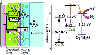
p-Type Co3O4 photocathodes with different amounts of CuO, were synthesized on fluorine doped tin oxide (FTO) via electrodeposition from a chloride bath containing suspended starch particles. All of the fabricated samples were photoresponsive toward water splitting in 0.5 M Na2SO4 under simulated sun-light. The PEC performance was evaluated using LSPV, chronoamperometry, and EIS techniques. The samples fabricated via the electrodeposition/anodizing/annealing process showed greater photocurrent response compared to the electrodeposition/annealing process. Among all the samples, the sample with an atomic composition% of Co: 24.9, Cu: 25.0 and O: 50.1 showed an optimum photocurrent response (∼6.5 mA cm−2 vs. SCE at −0.3 V). The structure, morphology/composition and optical response were characterized by XRD, FESEM/EDX and UV-Vis techniques, respectively.
1. Introduction
Photoelectrochemical (PEC) water splitting is a promising route for the clean generation of hydrogen fuel and oxygen. However the search for materials with a suitable band-gap (≥redox potential of water 1.23 eV) is a challenging task. Materials with semiconducting behavior are reported to exhibit photo responsive behavior toward water splitting due to the presence of an energy band-gap.1–3 Among the different types of semiconductors such as nitrides, sulfides, phosphides, selenides and tellurides, metal oxides have better stability in aqueous solution in a wide range of pH. Furthermore, a reasonable photocurrent density can be obtained from a metal oxide with a band-gap close to 1.23 V. The metal oxides with n-type and p-type behavior have been extensively investigated for water splitting applications as photoanodes and photocathodes, respectively. One of the most important metal oxides is cobalt oxide which has been used in super capacitors, biosensors, lithium batteries and photoelectrochemical devices.4–6 Numerous researchers have reported a wide range of band-gap values for p-type cobalt oxides with different structures (1.37–2.7 eV).6,7
Cobalt oxide has been fabricated by physical and chemical methods such as: hydrothermal, CVD, AACVD, electrophoretic and electrodeposition/annealing.8–11 However, the main limitation of cobalt oxide in solar driven water splitting is the energy consumption through the additional bias voltage. This drawback can be compensated once co-catalysts with a lower bang gap (e.g. CuO; ∼1.3 eV) are added to the cobalt oxide thin films. Recently, due to the lower cost and appropriate band-gap of copper oxide, it has been used as a highly effective semiconductor electrode in photoelectrochemical water splitting (PEC). However, pure copper oxide has lower stability unless mixed with other stable materials.12,13 Photocurrent response of metal oxides could be improved by increasing the active surface area through the fabrication of nano-sheets, mesopores, nanotubes and nanowires.5–14 In spite of the p-type behavior of Co3O4, it has been mostly used as a catalyst and co-catalyst for the oxygen evolution reaction (OER), but only few studies on cobalt oxides were reported for the photoelectrochemical hydrogen evolution reaction (HER).15–17
In the present work, we have fabricated a number of Co3O4–CuO thin films through the pulse-electrodeposition/anodization and annealing process. The thin films were obtained from cobalt and copper chlorides mixture of electrolytes (with suspended starch particles). The photoresponse and structural characterization of the fabricated films were also investigated.
2. Experimental methods
Electrode preparation
The fabrication of the p-type porous electrodes was performed using electrochemical and thermal techniques. The chemicals reagents (analytical grade) in this work were procured from Aldrich and used as received. Hierarchically, the cobalt oxide thin films fabricated on the fluorine doped tin oxide (FTO/from Pilkington company) glass (1 × 1 cm2) were prepared by the following steps:
(i) The FTO glasses were ultrasonically cleaned in acetone for 7 min, rinsed in distilled water and dried in an oven. (ii) The cobalt films (with different amount of copper) were electrodeposited on the FTO glass substrate, from a CoCl2·6H2O + CuCl2·2H2O electrolyte at pH = 4. A three compartment electrochemical cell with calomel as the reference electrode (RE), the fabricated thin films as the working electrode (WE) and a Pt mesh as the counter electrode (CE): were used in the electrochemical process. A potentiostat/galvanostat from AutoLab, model PGSTAT 240 interfaced with a computer, were used in this process. The layers were deposited using pulse chronoamperometry technique for 15 cycles with the following order, −10 mA cm−2 (10 s) and −6 mA cm−2 (5 s). The content of the electrolytes and the suspended starch (1.5 g L−1) are tabulated in Table 1. (iii) The same technique (chronoamperometry, +10 mA cm−2) was used for the anodization of the deposited layers in hydrogen peroxide (10%) for 10 min. (iv) Finally the anodized layers were annealed in 500 °C for 2 h in an open tube furnace to produce the Co3O4 and Co3O4–CuO layers.
Table 1 The fabrication conditions during the electrodeposition/anodization/annealing process and elemental composition from EDX
Sample series |
Sample name |
Electrodeposition |
Anodization in (10% H2O2) |
Annealing (500 °C) |
EDX/atomic% (Co : Cu : O) |
CoCl2·6H2O (mM L−1) |
CuCl2·2H2O (mM L−1) |
Starch (1.5 g L−1) |
(I) |
SA |
40 |
— |
√ |
— |
√ |
44 : 0 : 56 |
SB |
40 |
5 |
√ |
— |
√ |
33.9 : 20.3 : 45.8 |
SC |
40 |
10 |
√ |
— |
√ |
26.1 : 27.3 : 46.6 |
SD |
40 |
20 |
√ |
— |
√ |
12.8 : 31.7 : 55.5 |
(II) |
*SB |
40 |
5 |
√ |
√ |
√ |
36.8 : 18.4 : 44.5 |
*SC |
40 |
10 |
√ |
√ |
√ |
24.9 : 25.0 : 50.1 |
*SD |
40 |
20 |
√ |
√ |
√ |
10.5 : 29.7 : 59.8 |
*SD′ |
40 |
20 |
√ |
√ |
— |
13.1 : 37.6 : 47.3 |
Physical characterizations
The morphology and chemical composition of the photo-cathodes were investigated by field emission scanning electron microscopy (FESEM) and energy dispersive X-ray spectroscopy (EDX) (FESEM/EDX quanta 600), respectively. XRD (Bruker D8 discover diffractometer with Cu Kα radiation, λ = 1.540598 Å) was used to determine the crystalline structure of photo-cathodes. In addition, an UV-visible transmission spectrophotometer (Perkin Elmer lambda 650) was used to investigate the absorbance of the FTO coated samples using a bare FTO glass as the reference.
Photoelectrochemical (PEC) measurements
The PEC performance of the prepared cobalt oxide films was investigated in a photoelectrochemical cell with a quartz window (filled with 0.5 M Na2SO4). The PEC performance of the electrodes was measured in the dark and light illumination with a 150 W Xe lamp (100 mW cm−2). The linear sweep photo-voltammetry (LSPV) was run at 5 mV s−1 between 0.3 to −0.6 V. Chronoamperometry at 0 V for 30 min was performed to examine the stability of the fabricated electrodes, using the same electrode configuration in the LSPV. The aforementioned cell configuration and electrolyte were also used in the EIS measurements. The EIS measurements were performed at the open circuit potential condition with the Vrms of 10 mV and a frequency range between 100 kHz to 10 mHz, using the frequency response analyzer (FRA) software installed in a computer and interfaced with the Autolab 240 potentiostat/galvanostat. Alternatively, the Mott–Schottky plot were performed through the EIS technique at potential range (−0.2 to 0.3 V vs. SCE) with frequencies of 10, 1 and 0.1 kHz in the dark condition.
3. Results and discussions
The fabrication of the porous p-type semiconductor thin films was performed in the electrolytes with and without the starch suspension. The starch suspensions play an important role in the fabrication of the thin films. The numerous sites on the electrode surface were blocked by the starch particles, thus the nucleation and growth occurred on the free sites on the FTO substrate. Previous works have reported that porous thin films could be fabricated using in situ nanoparticles suspension which can be removed by chemical and thermal process.18–21 In the fabrication process, the starch particles were removed from the thin film surface during the water rinsing and annealing (500 °C) steps. During the penultimate process, the fabricated thin films were anodized in alkaline 10% hydrogen peroxide (pH = 9) at +10 mV cm−2 for 10 min. It was widely reported that the fabrication of metal oxide layers can be performed by the anodization technique in traditional alkaline electrolytes.22,23 An efficient anodization process could be performed in a mixture of hydrogen peroxide–alkaline solution. An oxygen rich electrolyte was achieved due to the decomposition of H2O2 in the presence of the metal surface. |
 | (1) |
|
 | (2) |
|
 | (3) |
The decomposition reaction of hydrogen peroxide was reported by James et al.24 a dark-green color was observed on the surface of the anodized thin films, which is due to the mixture of copper and cobalt oxide and hydroxide layers during the anodization. The anodization process was followed by annealing in an open tube furnace to convert the metals and metal hydroxides (dark-green) to metal oxide (black) at 500 °C for 2 h. The heat treatment process for the conversion of cobalt and copper hydroxide was widely studied by Mao et al., He et al., and Wu et al.15,25,26
Physical properties of fabricated electrodes
Structure characterizations. The structure of the fabricated thin films was characterized using X-ray diffraction technique. Fig. 1 shows the FTO (red), Co3O4/FTO (green) and Co3O4–CuO/FTO (violet) diffractograms. The XRD of Co3O4 (green) shows the (220), (311), (400), (511) and (440) planes at 31.2°, 36.7°, 44.7°, 59.1° and 65.2°, respectively. The peaks are attributed to the cubic spinel Co3O4 crystal (JCPDS 42-1467). It was proven that the green layer of Co(OH)2 from the anodization step was entirely converted to the black Co3O4 during the annealing process. The same phenomena were observed by Mao et al., and Wang et al.15,27 Fig. 1 is the XRD of Co3O4–CuO/FTO (violet) where it shows the appearance the CuO planes: (110), (−111), (111), (−202), (202), (−113) and (220), and shows good agreement with the standard XRD pattern of the monoclinic CuO (ICDD-JCPS file no. 05-0661). The same results were achieved by other researchers.13,28
 |
| Fig. 1 XRD pattern of (A) FTO, (B) Co3O4/FTO and (C) Co3O4–CuO/FTO. | |
SEM/EDX studies. The cross-sectional and surface morphology of the electrodeposited/anodized and post annealed samples are shown in Fig. 2. The top view of the non-anodized and anodized (in alkaline peroxide medium) samples are displayed in Fig. 2a and b, for *SB respectively. Under higher magnification (Fig. 2b), the appearance of nano-sheets can be clearly observed due to the anodization process. It was found that morphology with higher surface area can be achieved when the sample was anodized. The morphology of the sample (*SB) is displayed in Fig. 2c. Approximately, the thickness of the prepared samples was 3 μm, the cross-sectional image of a typical sample (*SB) is shown in Fig. 2d. Furthermore, the top view morphology of *SC and *SD was observed as image (e) and (f) in Fig. 2 respectively. The EDX spectrum of the samples is inserted at the corner of the corresponding image. The images show that different surface morphology can be achieved by varying the CuO content in the thin films. Interestingly, Fig. 2f shows the appearance of nano-dendrites with coconut leaf shape for *SD (atomic%: Cu: 29.7%, Co: 10.5%, and O: 59.8%). The XRD of Fig. 2f confirms the presence of CuO and Co3O4 in the thin films. The elemental compositions (EDX, %) of the thin films are tabulated in Table 1.
 |
| Fig. 2 FESEM images of *SB sample: (a) electrodeposited layer (b) electrodeposited/annealed layer. FESEM image of prepared samples (*SB, *SC and *SD) via the electrodeposition/anodization/annealing process are displayed as (c)/(d) (cross-sectional view), (e) and (f) respectively. | |
Optical study. The optical absorption behavior of the fabricated samples was studied by UV-visible spectrophotometer in the transmission mode. As illustrated in the UV-visible spectrum, light absorption increases from the near infrared region and the band width continues to the UV region (wavelength 400 nm). Furthermore, Fig. 3a shows a red shift with the increase of CuO in the Co3O4 based layers. From the UV-Vis spectrum, the direct (allowed) band gap was calculated from the (αhν)2 vs. hν plot (Fig. 3b),29 |
 | (4) |
and |
 | (5) |
where α is the absorption coefficient, l is the thickness of the film (in this case 3 μm) and A is the absorbance.29
 |
| Fig. 3 (a) The UV-visible diffuse reflection for SA, SB, and SC, (b) the allowed direct band gap for the samples. | |
The band gap of the Co3O4 (SA) was determined through the (αhν)2 vs. hν plot, as shown in Fig. 3b. It was found that two band gap values of 1.5 and 1.8 eV were obtained via the extrapolation on the x axis. The larger band gap corresponds to a charge transfer process from the valence band of O2− 2p to the conduction band of Co2+ 2d, and the smaller band gap is due to the charge transfer process from O2− 2p to the conduction band of the Co3+. These achievements are in close agreement with the literature value of Co3O4.15,30 The estimated band gap of SC and SD are 1.35 and 1.18 eV respectively, from the extrapolation on the x axis as well (Fig. 3b). It should be noted that the SC has the higher band gap value and is closer to the ideal band energy (1.23 eV) for the water splitting process.
PEC characterization
Photocurrent investigation. The photoelectrochemical performance of the thin film electrodes was evaluated in 0.5 M Na2SO4 between +0.3 to −0.6 V vs. SCE under simulated sunlight and dark conditions (Fig. 4).
 |
| Fig. 4 Current–potential curves (vs. SCE) for samples series I (SA, SB, Sc and SD) from 0.2 to −0.6 V in 0.5 M Na2SO4, in the absence and presence of illumination (100 mW cm−2). | |
Fig. 4 illustrates the I–V curves of the thin film samples in the dark and illuminated conditions. The performance of the thin film samples fabricated by the electrodeposition/annealing (without anodization) process were investigated by I–V plot in both dark and light conditions (Fig. 4). It was found that the current magnitude of all thin film samples increased once exposed to light. The photocurrent magnitude of the fabricated metal oxides is in the order of: Sc > SD > SB > SA. Fig. 4 demonstrates that the photocurrent was maximal when the CuO component in the Co3O4 thin film was optimal (atomic%: Co: 26.1, Cu: 27.3, O: 46.6). On the other hand, the photoresponse of Co3O4 layer (SA) was negligible compared to the fabricated Co3O4–CuO samples. The poor electron transport properties of the pure Co3O4 are due to the lower electron excitation rate from the valence band to conducting band under illumination. Prior to the annealing process, the electrodeposited samples (Co–Cu) were anodized in an alkaline hydrogen peroxide (10%) electrolyte at 10 mA cm−2 (10 min). The magnitude of the photocurrent response for sample series (II) is as good as samples series (I). The analogues of Fig. 4 and 5 show that although the magnitude order of the photocurrent response are the same for both sample series, the anodized/annealed samples (series II) shows higher photocurrent value compared to the annealed samples (series I). Furthermore, as shown in Fig. 5 the photocurrent sensitivity of the prepared samples (series II) was benchmarked in the flip-flop light condition. Fig. 5 illustrates that the onset of photocurrent begins from the positive potential (vs. SCE). In illuminated conditions, the photocurrent was maximal (∼2 mA cm−2) for *SC sample at 0 V vs. SCE, whereas, the *SA and *SD samples gave 1.7 and 0.6 mA cm−2 at the same potential, respectively. Fig. 5 shows that photocurrent peaks of the samples are *SB, *SC and *SD were slightly decreased at more negative potentials. Perhaps, this phenomenon is due to the decomposition (or electrochemical reduction) of CuO. Interestingly, it was found that the highest photocurrent (∼6.5 mA cm−2) was achieved for sample *SC at −0.3 V. To the best of our knowledge, higher photocurrent (compared to these results) has not been reported by other cobalt oxide based electrodes in 0.5 M Na2SO4.7,13,16,17,25
 |
| Fig. 5 LSPV (I–V vs. SCE) in flip-flop light (100 mW cm−2) conditions for samples series II in 0.5 M Na2SO4 from 0.3 to −0.5 V. | |
The photoresponse stability of the samples was benchmarked by chronoamperometry (i–t curves) at 0 V vs. SCE for 30 min in flip-flop light condition as shown in Fig. 6, where the photocurrent decays along of i–t curves for all samples. The photocurrent decay was approximately 50% for all examined samples (except *SD′) during the initial 30 min. This fact has been also reported by other researchers as well.31–33 The examined samples were rinsed and dried after 30 min, and it was found that the thin film color changed from grey/black to copper red during the chronoamperometry step. The same finding was reported by Sagu et al., and G-Esparza et al.32,33 The color change is due to the electrochemical reduction of the thin films which can be described by following equations:33
|
CuO + H2O + 2e− ⇆ Cu + 2OH−
| (6) |
|
2CuO + 2H+ + 2e− ⇆ Cu2O + H2O
| (7) |
 |
| Fig. 6 Photocurrent–time response of the photocathodes at 0 V vs. SCE under flip-flop light (100 mW cm−2) condition for samples series II in 0.5 M Na2SO4. | |
The photocurrent response of *SD′ (yellow line) samples was fabricated via the electrodeposition/anodization process (without annealing). The photocurrent performance of *SD′ (yellow line) is presented in Fig. 6. Among all samples, the photocurrent response of *SD′ shows the poorest stability, due to the decomposition rate of metal hydroxide was faster than metal oxide samples. With regards to the color changes (from red-dark to green-red-dark) and decreasing layer thickness, eqn (3) suggests that the fabricated metal hydroxide layers (by anodization) was partially reduced to M(OH)2(ad) and a fraction of that was depleted to the solution medium as M(OH)2(aq).
Electrochemical impedance measurements. EIS is a robust tool for the investigation of PEC properties which it is mostly presented by the Nyquist and Bode/phase plots.29 The Nyquist plots show that the fabricated electrodes are strongly affected by illumination at 0 V (vs. SCE) applied potential (Fig. 7a) in the aqueous solution (0.5 M Na2SO4). The diameter of the semicircle in the Nyquist plot shows that the overall charge transfer resistance decreases under illumination compared to the dark, for all samples. The EIS experimental data in the dark and light conditions were simulated and excellent fittings were obtained from the simulations, in the form of analog circuits34 visually, the identification of the corresponding electrical analog circuit for non-ideal curves is not convenient. The equivalent electrical circuit from the EIS simulations is shown in Fig. 7b. The equivalent electrical circuit consists of two relaxation times whether in dark or light condition. As observed in Fig. 7b, both loops in the equivalent circuit are in parallel configuration. The corresponding loop of the semiconductor (Rsc‖CPEsc) is in series with the interfacial resistance of the double layer/thin film (Rdl) and both of them are in parallel with the double layer capacitance (Cdl). For a more accurate representation of the capacitance behavior, the constant phase element (CPE) was used instead of a pure capacitor in the simulations. The impedance of a CPE (ZCPE) for a non-ideal circuit element is given as:34 |
 | (8) |
where f is applied frequency, j is imaginary number, Q = C if the exponent n = 1, and Q ≠ C if exponent 1 > n > 0. It must be noted that the capacitance behavior is approximated by Q, if the electrode surface is rough or when the dielectric property of the electrode components are heterogeneous.29 The detailed corresponding electro-kinetic elements for the samples are tabulated in Table 2. It is found that the charge transfer resistance of the semiconductor (Rsc) is in the order of: *SD(D) > *SC(D) > *SB(D) in the dark, whereas, the Rsc value decreases in the order of: *SD(L) > *SB(L) > *SC(L) under illumination. The LSPV (Fig. 5) correlates with the EIS results. The EIS results also emphasize that (*SC) shows the highest efficient response to light among of all samples. It is also noted that the capacitance values (CPEsc) of the samples decreases with Rsc, whether in light or dark. This could be due to the decrease in the charge accumulation across the electrical double layer region when the charge transfer process becomes more prominent, and is in agreement with the deduction of Lopes et al.34
 |
| Fig. 7 (a) The Nyquist plots of the fabricated samples (series II) in 0.5 M Na2SO4 (@ 0 V vs. SCE) in the dark (D) and under illumination (L). (b) Energy diagram of the fabricated semiconductor/electrolyte interface with the respective electrical equivalent circuit. (c) Schematic representation of the heterogeneous (Co3O4–CuO) with aqueous medium in illuminated condition. | |
Table 2 The EIS parameters from the simulation of the equivalent circuit model at bias-free potential vs. SCE
Samples |
Rs (Ω) |
Rdl (Ω) |
Cdl (μF) |
Rsc (Ω) |
Q (Yo)sc (μmho) |
n |
*SB(D) |
15.62 |
168.89 |
158.4 |
5303 |
135.52 |
0.78 |
*SB(L) |
11.74 |
10.44 |
11.8 |
2307 |
176.38 |
0.68 |
*SC(D) |
11.144 |
113.12 |
208.7 |
16 374 |
339.32 |
0.76 |
*SC(L) |
14.874 |
15.467 |
59.9 |
2072 |
104.76 |
0.73 |
*SD(D) |
11.55 |
39.85 |
49.1 |
19 290 |
424.82 |
0.81 |
*SD(L) |
10.77 |
33.27 |
11.9 |
3348 |
271.44 |
0.74 |
From the energy levels of the composite (Co3O4, and CuO), an energy level diagram was proposed (Fig. 7c). It can be demonstrated that the PEC water splitting is enhanced due to the electron donation from the conduction band of Co3O4 to the valance band of CuO at low bias potentials.35
The space charge capacitance of the semiconductor as a function of the applied potential is represented by the Mott–Schottky equation,36 which leads to determination of flat band energy (Efb):
|
 | (9) |
where
εr is the relative permittivity of the semiconductor,
ε0 is permittivity in vacuum,
A is the surface area,
e is the charge of an electron,
ND is the donor density,
k is Boltzmann constant,
T is the temperature, and
E is the applied potential.
Samples *SB and *SD were studied by M–S technique in 0.5 M Na2SO4 via following operation condition: potential window range (−0.2 to 0.3 V vs. SCE), frequencies 1000, 100, 10 Hz, dark condition. Fig. 8 shows a typical p-type behavior of fabricated semiconductors from the negative slopes of the curves at various frequencies (1000, 100 and 10). The Efb for the samples was determined from the extrapolation of the slope to potential axis. The estimated Efb (vs. SCE) for *SB and *SD are 0.71 and 0.53 V, respectively. These values are close to the results of Zhang and Wang for CuO.36
 |
| Fig. 8 Mott–Schottky plots for samples (*SB and *SD) in dark condition at frequencies (10, 1, 0.1 kHz). | |
4. Conclusion
Heterogeneous Co3O4–CuO photocathodes were successfully prepared via electrodeposition/anodization (in alkaline peroxide)/annealing in 500 °C on FTO. The performance of the fabricated electrodes toward PEC was examined with LSPV, chronoamperometry, and EIS techniques. The photocurrent value increases with the increase of CuO content in the thin films. Furthermore, the photocurrent performance of the photocathodes was enhanced with anodization in alkaline peroxide electrolyte before the annealing process. The thin films with the composition: Co: 24.9, Cu: 25.0, and O: 50.1% (*SC) gave the best photocurrent performance (∼6 and ∼2 mA cm−2 vs. SCE at −0.3 and 0 V, respectively). The band-gap values of the thin film samples were also determined, where the band gap of *SC was 1.35, which is suitable for hydrogen generation via the water splitting process.
Acknowledgements
The authors would like to thank the Ministry of Higher Education for the financial support from grants FRGS/2/2013/TK06/UKM/03/1 and FP033 2013A.
References
- M. Shao, F. Ning, M. Wei, D. G. Evans and X. Duan, Adv. Funct. Mater., 2013, 24(4), 580–586 Search PubMed.
- Y. Sun, C. Liu, D. C. Grauer, J. Yano, J. R. Long, P. Yang and C. J. Chang, J. Am. Chem. Soc., 2013, 135, 17699–17702 CrossRef CAS PubMed.
- E. J. Popczun, J. R. McKone, C. G. Read, A. J. Biacchi, A. M. Wiltrout, N. S. Lewis and R. E. Schaak, J. Am. Chem. Soc., 2013, 135(25), 9267–9270 CrossRef CAS PubMed.
- F. D. Wu and Y. Wang, J. Mater. Chem., 2011, 21, 6636–6641 RSC.
- C. Guan, J. P. Liu, C. W. Cheng, H. X. Li, X. G. Li, W. W. Zhou, H. Zhang and H. J. Fan, Energy Environ. Sci., 2011, 4, 4496–4499 CAS.
- H. S. Jeon, W. Park, J. Kim, H. Kim, W. Kim and B. K. Min, Int. J. Hydrogen Energy, 2011, 36, 1924–1929 CrossRef CAS PubMed.
- J. Chen and A. Selloni, J. Phys. Chem. Lett., 2012, 3(19), 2808–2814 CrossRef CAS.
- T. Maruyama and T. Nakai, Sol. Energy Mater., 1991, 23(1), 25–29 CrossRef CAS.
- E. D. Lester, G. Aksomaityte, J. Li, S. Gomez, J. Gonzalez-Gonzalez and M. Poliakoff, Prog. Cryst. Growth Charact. Mater., 2012, 58(1), 3–13 CrossRef CAS PubMed.
- D. Zhang, X. Li, X. Guo and C. Lai, Mater. Lett., 2014, 126, 211–213 CrossRef CAS PubMed.
- M. S. Hill, A. L. Johnson, T. D. Manning, K. C. Molloy and B. J. Wickham, Inorg. Chim. Acta, 2014, 422, 47–56 CrossRef CAS PubMed.
- S. Choudhary, A. Solanki, S. Upadhyay, N. Singh, V. R. Satsangi, R. Shrivastav and S. Dass, J. Solid State Electrochem., 2013, 17, 2531–2538 CrossRef CAS PubMed.
- R. Patil, S. Kelkar, R. Naphade and S. Ogale, J. Mater. Chem. A, 2014, 2, 3661–3668 CAS.
- X. Yang, A. Wolcott, G. Wang, A. Sobo, R. C. Fitzmorris, F. Qian, J. Z. Zhang and Y. Li, Nano Lett., 2009, 9(6), 2331–2336 CrossRef CAS PubMed.
- Y. Mao, W. Li, P. Liu, J. Chen and E. Liang, Mater. Lett., 2014, 134, 276–280 CrossRef CAS PubMed.
- J. Wang and F. E. Osterloh, J. Mater. Chem. A, 2014, 2, 9405–9411 CAS.
- L. J. Zhou, Y. Zou, G. D. Li, X. Zou, J. Zhao, M. Fan, Y. Liu and D. Wang, RSC Adv., 2014, 4, 22951–22954 RSC.
- J. H. Kim, S. H. Kang, K. Zhu, J. Y. Kim, N. R. Neale and A. J. Frank, Chem. Commun., 2011, 47, 5214–5216 RSC.
- W. Li and J. Y. Walz, Sci. Rep., 2014, 4, 4418 Search PubMed.
- Y. Nishijima, K. Ueno, S. Juodkazis, V. Mizeikis, H. Fujiwara, K. Sasaki and H. Misawa, Opt. Express, 2009, 17(4), 2976–2983 CrossRef CAS.
- G. Subramanian, V. N. Manoharan, J. D. Thorne and D. J. Pine, Adv. Mater., 1999, 11(15), 1261–1265 CrossRef CAS.
- S. John, V. Balasubramanian and B. A. Shenoi, Surf. Technol., 1985, 26(3), 207–216 CrossRef CAS.
- L. Ling-ling, C. Ying-liang, W. Hui-min and Z. Zhao, Trans. Nonferrous Met. Soc. China, 2008, 18, 722–727 CrossRef.
- S. J. D. Mitchell, J. P. Farr and D. T. Carty, EP0209228 Al, 1987.
- J. He, Y. Peng, Z. Sun, W. Cheng, Q. Liu, Y. Feng, Y. Jiang, F. Hu, Z. Pan, Q. Bian and S. Wei, Electrochim. Acta, 2014, 119, 64–71 CrossRef CAS PubMed.
- X. Wu, H. Bai, J. Zhang, F. Chen and G. Shi, J. Phys. Chem. B, 2005, 109, 22836–22842 CrossRef CAS PubMed.
- X. Wang, X. Dong, Y. Wen, C. Li, Q. Xiong and P. Chen, Chem. Commun., 2012, 48, 6490–6492 RSC.
- W. Wang, L. Wang, H. Shi and Y. Liang, CrystEngComm, 2012, 14, 5914–5922 RSC.
- Z. Chen, H. N. Dinh and E. Mille, Photoelectrochemical Water Splitting Standards, Experimental Methods, and Protocols, Springer, New York, Heidelberg, Dordrecht, London, 2013 Search PubMed.
- F. Gu, C. Li, Y. Hu and L. Zhang, J. Cryst. Growth, 2007, 304(2), 369–373 CrossRef CAS PubMed.
- A. Paracchino, V. Laporte, K. Sivula, M. Grätzel and E. Thimsen, Nat. Mater., 2011, 10, 456–461 CrossRef CAS PubMed.
- J. S. Sagu, T. A. Nirmal Peiris and K. G. UpulWijayantha, Electrochem. Commun., 2014, 42, 68–71 CrossRef CAS PubMed.
- A. T. Garcia-Esparza, K. Limkrailassiri, F. Leroy, S. Rasul, W. Yu, L. Lin and K. Takanabe, J. Mater. Chem. A, 2014, 2, 73–89 Search PubMed.
- T. Lopes, L. Andrade, H. A. Ribeiro and A. Mendes, Int. J. Hydrogen Energy, 2010, 35, 11601–11608 CrossRef CAS PubMed.
- J. Barber and P. D. Tran, J. R. Soc., Interface, 2013, 10(81), 20120984 CrossRef PubMed.
- Z. Zhang and P. Wang, J. Mater. Chem., 2012, 22, 24–56 Search PubMed.
|
This journal is © The Royal Society of Chemistry 2015 |
Click here to see how this site uses Cookies. View our privacy policy here.