Jun Pua,
Lei Tanga,
Chaowei Lia,
Taotao Lia,
Lin Lingab,
Kai Zhanga,
Qingwen Lia and
Yagang Yao*a
aKey Lab of Nanodevices and Applications, Suzhou Institute of Nanotech and Nanobionics, Chinese Academy of Sciences, University of Chinese Academy of Sciences, 398 Ruoshui Road, Suzhou Industry Park, Suzhou 215123, P. R. China. E-mail: ygyao2013@sinano.ac.cn; Fax: +86-512-62872552; Tel: +86-512-62872829
bSchool of Chemical and Material Engineering, Jiangnan University, Wuxi 214122, P. R. China
First published on 12th May 2015
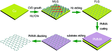
The layer numbers of graphene for graphene based transparent conductive films are crucial. An appropriate number of graphene layers would provide excellent electrical conductivity along with high transparency. Herein, we demonstrated a facile and scalable technique to grow graphene with controllable layers on copper foil substrates using the etching effect of H2 in atmospheric pressure chemical vapor deposition (APCVD), and studied the influence of H2 etching on the properties of graphene transparent conductive films. The etching of formed multi-layer graphene (MLG, 12–14 layers) for Cu substrates assists the formation of few-layer graphene (FLG, 2–3 layers). These as-obtained graphene can be used as high performance transparent conductors, which show improved tradeoff between conductivity and transparency: the transmittance of 96.4% at 550 nm with sheet resistance of ∼360 Ω sq−1, and the transmittance of 86.7% at 550 nm with sheet resistance of ∼142 Ω sq−1. They could be used as high performance transparent conductors in the future.
Among the numerous ITO alternative materials, graphene is a two-dimensional (2D) nanomaterials of sp2-hybridized carbon atoms bonded together in a hexagonal lattice, which has many extraordinary properties, such as large specific surface area (∼2630 m2 g−1), large Young's modulus (∼1100 GPa), high charge carrier mobility (∼200000 cm2 V s−1), and high thermal conductivity (∼5000 W m−1 K−1).8–11 The excellent properties in the π-conjugated two-dimensional electron system make graphene a promising candidate for widespread applications in different areas, such as post-silicon electronics,12 displays,13 energy storage devices,14 and sensors.15 Therefore, graphene is one of the most potential materials for transparent conductive films due to its optical transparency over a wide range of wavelengths and high electrical conductivity.16,17 In the past few years, many reports have demonstrated that graphene has the lead in this field.18,19 Zhang et al. reported that the graphene prepared by chemical vapor deposition (CVD) on tilted copper foil, showed the transmittance of 96.5% at 550 nm with sheet resistance of 600 Ω sq−1 (1–3 layers), and the transmittance of 86.7% at 550 nm with sheet resistance of 400 sq−1 (5–6 layers). Cheng et al. found an efficient way to make large-area graphene oxide sheets with a sheet resistance of 840 Ω sq−1 and 78% transmittance at 550 nm. Despite of these excellent performances, it is flawed because the properties of graphene are very sensitive to its layer numbers.20 The transmittance increases with superposition of single-layer graphene sequentially, and as a result, as graphene film gets thicker, the transparency is expected to decrease. On the contrary, the sheet resistance of graphene film decreases with the increase of graphene layer.21,22 For this reason, few-layer graphene (FLG) should have advantages of both high diaphaneity and low resistance together. Therefore, it is highly desirable to synthesize FLG in a large scale to unlock its valuable properties.
A series of approaches to synthesis graphene films have been developed, including mechanical exfoliation, CVD, epitaxial growth, and oxidation–reduction process. Among various graphene synthesis methods, CVD is promising, because it has the capability of making large-scale graphene films with outstanding electrical conductivity and field-effect mobility properties.23–25 Meanwhile, methane or other hydrocarbons gas all can be used as carbon source to obtain high quality graphene, which is convenient and feasible.26 Specially, in high vacuum conditions by controlling the diffusion of carbon species extended monolayer graphene can be achieved with high surface coverage.27 Unfortunately, the expensive vacuum system may be an inhibiting issue. In general, H2 seems to serve a dual role in CVD growth of graphene: as a cracking activator of the carbon source on surface; as an etching reagent that controls the size and thickness of the graphene domains.28 So, how to tune these two kinds of effects of H2 in order to make FLG with high diaphaneity and low resistance in the CVD process will be a very interesting subject. Skákalová and co-workers synthesized the FLG by CVD on Ni-coated Si substrates under a continuous flow of carrier gases, Ar and H2, mixed with less than 5 vol% methane (CH4:
Ar
:
H2 = 250
:
1000
:
4000 sccm), and they explored the influence of reaction time (30 s and 7 min) on the products during the CVD process.24 In the present work, we demonstrated an easy strategy to produce FLG (2–3 layers) through etching effects of H2 in the CVD growth of graphene film on Cu substrate. In addition, more experiment parameters which could affect the final products such as the gas flow rate and etching time were investigated. Such graphene films were transferred by poly(methyl methacrylate) (PMMA) and exhibited good sheet resistance and high transparency in the range of 360 Ω sq−1 at 96.4% transparency and 142 Ω sq−1 at 86.0% transparency, respectively. We believe that the demonstrated strategy will promote the synthesis of high performance transparent conductive graphene films at large scale and its real applications.
Optical micrographs of Cu surface after 30 min annealing and the as-prepared FLG (sample no. 10) are shown in Fig. 2a and b. It is clearly seen that the Cu surface is smooth through 30 min annealing at 1000 °C. After growth and etching processes, Cu substrate was covered with FLG thin film. Fig. 2c shows the SEM image of MLG without the etching section (sample no. 1: H2 500 sccm, CH4 10 sccm for 10 min growth). Hexagonal graphene grows uniformly across the growth substrate. There are many dense carbon dots by observing carefully, which may be the nucleation point for graphene.32 In this CVD period, H2 could in-diffuse into the Cu substrate and compete with CH4 for chemisorption. Besides, the H2 can also passivate defects and grain boundaries.33,34 After the additional etching process (H2 50 sccm for 30 min), it can be seen that the density of these carbon dots decreased, indicating that H2 also etched the carbon points. Fig. 2d and e reveal the typical SEM of inceptive hexagon-shaped graphene grown on Cu substrate under the condition of etching with H2 50 sccm for 30 min. The size of FLG structure is around 3 μm with good uniformity. A higher magnification SEM image in inset of Fig. 2e displays a wrinkled structure on the graphene surface, which most likely arises from the different thermal expansion coefficients between copper and graphene.3,35 The hexagon edges appear as straight lines and the angles between adjacent edges are all 120°. Fig. 2f shows the typical Raman spectra of these two samples of graphene grown on Cu (sample no. 1 and 10). All grey flakes showed single layer characteristics of graphene, characterized by two peaks located around 2686–2700 cm−1 and 1581 cm−1, which reveal that MLG was transformed to FLG by H2 etching for 30 min. The as-prepared MLG and FLG were further characterized by HRTEM, and the resulting images are displayed in Fig. 2g and h, respectively. Obviously, the layer number of the MLG sample was confirmed to be around 12 to 14 layers, whereas the FLG was comprised of 2 to 3 layers. The inset of Fig. 2g shows the SAED of MLG. It can be seen that the multideck graphene film demonstrates weak two-dimensional hexagonal packing due to the superposition of many single layer graphene. On the contrary, the SAED result of 2–3 L graphene exhibits a disordered AB stacking between layers (inset of Fig. 2h).
In order to explore the etching time effect, the evolution of the G/2D intensity ratio is monitored by varying the etching time from 0 to 90 min under the same conditions (H2 50 sccm), which shown in Table S1† (the samples from no. 1 to no. 13). According to the spectrum diagrams in Fig. S1,† it can be seen that a lower intensity ratio of G/2D is observed with the extension of etching time.
The amount of H2 in the etching process also plays an important role on the final graphene products. The SEM results display in Fig. 3 are that the samples prepared by additional etching with 80 and 100 sccm H2 for 30 min. Careful analysis of these images reveals an important fact that both average size and density of etched area monotonically increase with time, indicating the deterioration of H2 etching. The inset in Fig. 3b shows typical individual etched pattern obtained at large flow rate of H2. In this stage, etching starts from the edge of the hexagon (the large white area), and then gradually spread to the center. Thus the graphene become like snowflake (the small white and dark area), and the snowflake-like sample finally disappear as time extends. This observation is consistent with previous literatures.36,37
![]() | ||
Fig. 3 The SEM images of graphene after etching for 30 min under 80 sccm H2 and 100 sccm H2. The inset in (b) shows typical etched pattern. |
In addition, a little amount of CH4 was introduced in the additional etching step to weaken the H2 etching for obtaining high uniformity FLG. Thus, a series of experiments was carried out with various H2/CH4 flow rate ratios in the etching process to optimize the amount of introduced CH4 and the total etching time (the samples from no. 14 to no. 30, see Table S1†). More continuous films were prepared as shown in Fig. S2† with the existence of 0.2 sccm CH4 during the etching process, but the Raman spectra show that these graphene (sample no. 16–18) were multi-layer, though the G/2D intensity ratio is decreasing with the increase of the etching time. Small amount of etching area appeared at the etching time of 60 min and the inset of Fig. S2c† shows a high magnification SEM image of one part of the etched area. It was found its shape was different with the snowflake morphology observed above, which was most likely due to the presence of CH4. Afterwards, the H2 amount was increased in order to achieve FLG. Graphene samples from no. 19 to no. 21 were synthesized with higher flow rate of H2 (80, 100, and 150 sccm). As shown in Fig. S3,† with the increase of flow rate of H2, the average size and density of etched graphene (white area) on Cu surface increased as well, proving the corrosion ability of H2 is stronger. When flow rate of H2 was increased to 150 sccm, FLG was achieved as Raman spectra proved in Fig. S3d,† revealing that with the increase of H2, etching effect becomes more obvious. However, the graphene film obtained by high H2 etching became discontinuous due to the larger etched area as shown in Fig. S3c,† which is unfavorable for graphene's applications. In the case of samples from no. 22 to no. 27 with increasing the CH4 amount while keeping the H2 amount at 50 sccm, the Raman results show that when increasing the CH4 to 0.4 or 1 sccm, no matter how longer the etching time is (30, 60 or 90 min), the as-obtained graphene were all multi-layer.
Furthermore, we also tried to lower the growth time in the first CVD process while keeping the H2 amount of 50 sccm in the etching process (samples from no. 28 to no. 30) to thin the layers of graphene. However, we were not able to achieve continuous FLG. It can be clearly seen from the SEM and Raman results shown in Fig. S5† that the density of etched area is larger, which is not beneficial for transparent conductive films. When the etching time was increased to 90 min, the graphene were completely etched away (Fig. S5c†), confirming the existence of the H2 etching effect.
High-quality FLG and MLG synthesized above allow us to investigate graphene's potential application as transparent conductive films. After transferring FLG to glass or Si substrates by PMMA-assisted method, Raman spectroscopy was used to characterize the quality and thickness of the as-transferred graphene samples of FLG (sample no. 10) and MLG (sample no. 1). The results are revealed in Fig. 4. Graphene has two typical Raman characteristics peaks, G band at about 1580 cm−1 and 2D band at about 2670 cm−1, which belong to the in-plane vibrational mode and the intervalley double resonance scattering around the K-point of the Brillouin zone, respectively.38–40 In addition, there are other two defects induced peaks at about 1340 and 1620 cm−1 in obtained Raman curves. Defects through an intervalley double-resonance Raman process activated the D band (1340 cm−1). While the D′ band (1620 cm−1) is assigned to the intravalley double-resonance process.35 The Raman spectrum of as-transferred FLG in Fig. 4a shows lower D peak, sharper G peak, higher and more intense 2D peak, and a lower G/2D intensity ratio (0.8) than that of MLG without the H2 etching process. These features are consistent with previous reports, indicating that the sample is FLG and MLG, respectively.41–43 Fig. 4b reveals the local Raman data of 2D peak position. With the increase of graphene layers, half peak width of 2D peak increases, and it also has a blue shift phenomenon, which agree with the results in Fig. 2f. In this figure, the 2D peak shifts from 2681.7 cm−1 to 2690.6 cm−1, which confirms that during the additional period of H2 exposure, MLG was transformed to FLG by H2 etching.
![]() | ||
Fig. 4 Raman spectroscopy of the as-transferred MLG and FLG: (a) typical survey spectra; (b) Raman data of 2D peak position. |
The functional groups and electronic state of the elements of graphene were determined using the XPS technique. The XPS results of N element of graphene before and after transfer are shown in Fig. S6.† Only a little bit of N elements are obtained, and these N are generated from residual PMMA or the doping from Fe(NO3)3. Fig. 5 proves the C 1s core level spectrum of graphene before and after transfer. The C 1s spectra can be divided into a CC peak at 284.6 V and a C–C bond at 285.1 V, assigned to C sp2 and C sp3 bonds, respectively. This phenomenon may be due to the existence of both amorphous graphitic carbon and defects.44,45 However, the distinction of the two XPS spectra is that the spectrum of transferred graphene includes two other chemical bonds (286.5 V and 289.1 V), which are associated with the bonding of carbon atoms in polymer backbone and the methoxy function group, probably because of the PMMA residues on the graphene surface inevitably.46
The quality of graphene after transfer is a major concern when it is intended for use in transparent conductive electrode-based applications.47 UV-Vis spectrometer and four-probe sourcemeter were used to characterize the transmittance and sheet resistance. UV-Vis spectra exhibit the diaphaneity of as-prepared graphene films as wavelength of the incident light with a blank coverslip used for background subtraction (see Fig. 6a). It can be seen that transmittance of graphene in high band region is high, and goes down with the decrease of the band. At 550 nm, the as-obtained FLG film exhibits a high transmittance of 96.4%, higher than primitive MLG without H2 etching (89.6%), further indicating that the luminousness of graphene films could be improved by creating the additional stage of H2 etching to thin the graphene layers. The sheet resistances for MLG and FLG are 142 and 360 Ω sq−1, respectively. Fig. 6b presents a comparison of transparent conductor performances (sheet resistance and transmittance) of as-grown graphene films with previously reported graphene films. Our results show a significant increase in tradeoff between conductivity and transparency, which indicates that as-grown graphene can be used as transparent conductors, and also prove H2 etching of graphene layers. The as-obtained graphene exhibit a better property compared with the previous reports by Zhang et al. (transparency of 86.7–96.5%, and sheet resistance of 400–600 Ω sq−1),18 Ahn et al. (transparency of 80–95%, and sheet resistance of 510–280 Ω sq−1)42 and Rodney S. Ruoff et al. (transparency of 93–97%, and sheet resistance of 350–980 Ω sq−1).48 However, our results were poorer than these reports by Lee (transparency of 97.7%, and sheet resistance of 210 Ω sq−1) and Bae (transparency of 90.1–97.4%, and sheet resistance of 30–145 Ω sq−1),49,50 revealing that there is still a room for improving the quality of the graphene grown by CVD for use in transparent conducting electrode applications.
![]() | ||
Fig. 6 (a) The transmittance curves of graphene films transferred on glass substrate (sample no. 1, 10, 17, 22 and 25); (b) comparison of sheet resistance versus light transmittance at 550 nm. |
Fig. 6b shows the sheet resistance as a function of the optical transmittance. As shown in this curve, the electrical conductivity and light transmittance present a inversely proportional relationship, where the relationship between sheet resistance and transmittance generally agree with the Beer–Lambert rule.47,51 According to the Beer–Lambert law, the transmittance of light (T) through a homogeneous material can be obtained from the following equation:
T = e−αd | (1) |
![]() | (2) |
![]() | (3) |
In general, it can be used in real life as long as the square resistance of transparent conductive film is less than 300 Ω and transparent rate is higher than 85%. Therefore, the results present a significant improvement of conductivity and transparency, demonstrating that as-developed method of FLG preparation can replace ITO as a new generation of transparent conductive films for optoelectronic devices in the future.
Footnote |
† Electronic supplementary information (ESI) available. See DOI: 10.1039/c5ra03919c |
This journal is © The Royal Society of Chemistry 2015 |