A general method for the preparation of a thickness-controllable fluoro-containing organic film as a solid lubricant

Hongyu Liangab, Yongfeng Buc, Jianning Dingd and Junyan Zhang*a
aState Key Laboratory of Solid Lubrication, Lanzhou Institute of Chemical Physics, Chinese Academy of Sciences, Lanzhou 730000, China. E-mail: zhangjunyan@licp.cas.cn; Fax: +86 9314968295; Tel: +86 9314968295
bUniversity of Chinese Academy of Sciences, Beijing 100049, China
cKey Laboratory of Mesoscopic Chemistry of MOE and Jiangsu Provincial Lab for Nanotechnology, School of Chemistry and Chemical Engineering, Nanjing University, Nanjing 210093, China
dCenter for Low-Dimensional Materials, Micro-Nano Devices and System, Jiangsu Key Laboratory for Solar Cell Materials and Technology, Jiangsu Collaborative Innovation Center of Photovoltaic Science and Engineering, Changzhou University, Changzhou 213164, China

Received 5th March 2015 , Accepted 16th April 2015

First published on 16th April 2015


Abstract

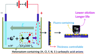
This research presents a general electrophoretic deposition (EPD) method, which offers selective preparation of various heteroatom-containing (i.e., H, Cl, F, N, and S) carboxylic acid molecular (CAM) films directly on silicon wafers, as long as the precursors are water-soluble carboxylic acids. Among them, the as-prepared fluoro-carboxylic acid (trifluoroacetic acid) molecular film with controllable thickness exhibits a longer wear life than self-assembled monolayers (SAMs), along with very low friction coefficient and a superior tolerance to humidity. It may be a promising candidate to replace SAMs as a more wear-resistant solid lubricant in micro/nano electromechanical systems (MEMS/NEMS).


1. Introduction

Due to the fact that the current parts of silicon-based micro/nano electromechanical systems (MEMS/NEMS) have poor wear resistance, placing one solid lubricant layer onto a silicon surface becomes a good approach to solve this problem.1,2 In consideration of the micro/nano-scale size of MEMS/NEMS components, coating a lubrication layer on such small parts with many nano-scale edges and corners is much more difficult than any parts of traditional mechanical systems. Traditional methods, such as magnetron sputtering techniques and plasma-enhanced chemical vapor deposition (PECVD), are unable to meet these microscopic lubrication demands.3 Self-assembly methods were considered to be suitable solutions to prepare ultra-thin lubrication layers for MEMS/NEMS because of their monomolecular thickness and good coverage to nano-scale locations.4–7 However, the SAM films are usually too thin (only several nanometers) to endure a long running time for MEMS/NEMS moving parts.8–10 Therefore, to prepare a thicker film with good coverage to nano-size parts becomes an imperative desire.

Electrophoretic deposition (EPD) techniques combine the merits of high controllability in thickness and excellent coverage to nano-scale edges and corners.11 However, the problem of how to drive the organic molecules by an electric field remains. As is well known, negatively charged graphene oxide (GO) sheets owing to the ionization of the carboxyl groups can migrate toward the anode under an electric field.12 Consequently, the carboxylic acid molecules, which are negatively charged by their own ionized anions in water, should also move to the anode. Therefore, we speculate that organic acids that are ionizable in water such as trifluoroacetic acid (TFA) can be used as fluoro-containing precursor materials to fabricate low-stiction and thicker organic molecular films.

In this study, thickness-controllable fluoro-containing carboxylic acid molecular films have been conveniently prepared directly on silicon wafers by EPD techniques. Tribological tests exhibit that the thicker films have longer wear lives and ultra-low surface stictions, along with superior resistance to humidity. Importantly, we have also examined other fluoro-monocarboxylic acids with longer carbon chains, which can also be employed to prepare advanced carboxylic acid molecular (CAM) films by EPD techniques. For instance, perfluorocaprylic acid was chosen as a precursor, and the corresponding films indeed displayed very low friction coefficients and wear rates. As such, other precursors with side carbon chains (citric acid) and chlorine-containing (trichloroacetic acid),13 nitrogen-containing (ethylenediaminetetraacetic acid), sulfur-containing (2,5-thiophenedicarboxylic acid), and aromatic benzene-containing (salicylic acid and pyromellitic acid) monocarboxylic or multicarboxylic acid molecules were also proved. These results further demonstrated that the EPD technique is a general method for preparing organic CAM films. Their unique features of selectable heteroatom doping and carbon skeletons create a great opportunity for the regulation of tribological properties of organic films to meet increasing lubrication requirements in MEMS/NEMS.

2. Experimental

2.1 Materials and preparation of the films

Trifluoroacetic acid (TFA) was purchased from Shanghai Sanyou Chemical Reagent Factory. N-type polished single-crystal silicon (100) wafers with resistivity of 0.01 Ω m were purchased from MCL Electronic Materials, Ltd. Ultrapure water (>18 MΩ cm) was used throughout the experiments. Initially, all silicon wafers were cleaned in a piranha solution (a mixture of 98% H2SO4 and 30% H2O2 with the ratio of 7[thin space (1/6-em)]:[thin space (1/6-em)]3 (v/v)), and then washed with ultrapure water several times and blown dry with N2. In a deposition experiment, two symmetric silicon wafers as working electrodes were immersed into a beaker containing 3.0 mmol L−1 aqueous solution of TFA with a constant distance of 5 mm, and then they were connected to a tunable DC power source. The corresponding films deposited at various voltages (20 V, 25 V, 30 V, 35 V and 40 V) on the anode for an hour were denoted as TFAF20, TFAF25, TFAF30, TFAF35 and TFAF40, respectively. All the experiments were conducted at room temperature.

2.2 Characterization

The values of zeta potential and conductivity of the aqueous solutions of TFA were measured by a Laser dynamic scattering tester (Nano ZS3600, Malvern, England). The morphologies of the films were observed by a microscope (Olympus, Japan) and atomic force microscopy (Veeco Nanoscope IIIa, USA), and the thicknesses were obtained by a L116-E ellipsometer (Gaertner, America), which was equipped with a He–Ne laser (632.8 nm) set at an incident angle of 50°. The surface roughness was also obtained by an atomic force microscope (Veeco Nanoscope IIIa, USA). In addition, transmission electron microscopy (TEM, JEM-1200EX, JEOL, Japan) and X-ray photoelectron spectroscopy (XPS, ESCALAB 250Xi, Thermo Scientific) were employed to reveal the structure and component of the films. Contact angle measurements were conducted by a Kruss DSA100 contact angle measuring instrument (Germany). Surface energies of the films were calculated with the methods described in the ESI. The adhesion (stiction) was measured by AFM (AIST-NT, Smart-SPM, USA) using a tip with a curvature radius of 10–25 nm and a normal force of 1.33 nN. The elastic modulus of the films was measured by a nanoindenter (TI-950, Hysitron, USA) equipped with a Berkowich diamond tip, which is a three-sided pyramid with a tip angle of 142.3°. The stress was obtained by a stress distribution tester (BGS 6341, China).

Tribological tests were performed on a rotary friction tester (MS-T3000, China) at room temperature in ambient air. The tested sample was fixed on a rotary sample stage at a rotation rate of 32 rpm, corresponding to a sliding velocity of 0.01 m s−1 under a normal load of 20 mN using a steel ball (φ = 3 mm) as the stationary upper counterpart. However, for the wear life experiment, the load was increased to 200 mN. To compare friction behavior, we also investigated a bare silicon wafer under the same conditions. The resulting worn tracks were measured using a dual-mode surface three-dimensional profiler (AEP, USA). The wear volume was calculated as V = AL, where A (mm2) is the cross-sectional area of worn scar and L (mm) is the length of the worn scar. The specific wear rate, W = V/SF, is determined as a function of the wear volume V (mm3) divided by the sliding distance S (m) and the applied load F (N). All the tests were performed at least three times to ensure data repeatability.

3. Results and discussion

3.1 Characterization of the films

Ionization is a common behavior of organic acids in an aqueous solution. Trifluoroacetic acid (TFA) is a strong monocarboxylic acid that can be easily ionized in an aqueous solution. Fig. 1a shows that the zeta potential values of TFA solutions are all negative over the entire concentration range, and the corresponding conductivities increase with concentration. This confirms that the TFA molecules are negatively charged in an aqueous solution, and can migrate to the anode under a uniform electrical field. According to this principle, the detailed electrophoretic deposition system was designed, as shown in Fig. 1b. Two symmetric silicon wafers with a constant distance of 5 mm were immersed into a beaker containing 3.0 mmol L−1 aqueous solution of TFA. When they were connected to a DC power source, a series of TFA films (TFAF20, TFAF25, TFAF30, TFAF35 and TFAF40) deposited at different voltages (20 V, 25 V, 30 V, 35 V and 40 V) can be fabricated on the silicon substrates of the anode.
image file: c5ra03900b-f1.tif
Fig. 1 (a) Zeta potential and conductivity of TFA solutions at various concentrations. (b) Schematic of electrophoretic deposition system for TFA films.

As shown in Fig. 2a, the as-prepared films appear to be homogeneous and smooth, and their color varies with increasing voltage (20–40 V). The corresponding AFM images (Fig. 2b) show that these films are composed of uniform nanoparticles, and the size increases with the applied voltage. The changes in color and size of nanoparticles imply the variations in film thickness, which was confirmed by measuring their thickness. The thickness of TFAF20, TFAF25, TFAF30, TFAF35 and TFAF40 is 59.0 nm, 93.0 nm, 122.0 nm, 175.9 nm and 234.8 nm, respectively, as shown in Fig. 2c, which nearly increases linearly with voltage (20–40 V). These results demonstrate that thickness-controllable TFA films with homogeneous surfaces can be easily obtained by electrophoresis techniques. To further reveal the microstructure of the films, TEM was conducted for TFAF30, and the corresponding image (Fig. 2d) shows that TFAF30 is composed of amorphous aggregations with unordered nano-chains, which may be caused by the electropolymerization of organic acid molecules. In the high-resolution C 1s spectrum of TFAF30 (Fig. 2e), two peaks at ∼284.6 eV and ∼288.2 eV correspond to C–C bonds with sp2 configuration and C–F bonds (see the enlarged image in Fig. 2e), respectively.14 A typical full spectrum of the film deposited at 30 V is shown in Fig. 2f, indicating that the film is mainly composed of C, F and O elements (Si signals come from silicon substrate). The inset image in Fig. 2f is the corresponding F 1s spectrum; the peak at ∼686.2 eV demonstrates that the fluorine in the film originates from the F–C bonds rather than fluoride ions,15,16 and the ratio of F/C is ∼2.7%. The abovementioned XPS spectra suggest that the as-prepared films are indeed fluoro-containing molecular films. In addition, the full spectra of the other four films are given in Fig. S3, which shows that all of them have the same composition.


image file: c5ra03900b-f2.tif
Fig. 2 (a) Optical and (b) AFM images of the films deposited at different voltages (20–40 V). (c) Thicknesses of the films as a function of voltage. (d) TEM image of the film deposited at 30 V. (e) C 1s (inset is an enlarged image of the C–F bond) and (f) XPS full spectrum of the film deposited at 30 V (inset is the corresponding F 1s spectrum).

3.2 Tribological study of the films

The tribological properties of the films were investigated by a rotary friction tester, as shown in Fig. 3a. With the increase in voltage, the friction coefficients first increase and then decrease. The trend in the variation of friction coefficient is summarized in Fig. 3b. It can be seen that the film deposited at 30 V (TFAF30) has the lowest friction coefficient (0.047), which is only about 1/13 of bare Si wafer (0.62) (Fig. S1a). Even compared to low-friction SAMs, which are self-assembled with long carbon-chain perfluoroalkylsilane molecules,17 the friction coefficients of TFA films are one order of magnitude less (0.12, when normal load was 5–20 mN). In this regard, the optimal deposition voltage is 30 V. This may be due to the unique surface properties (stiction, roughness, and contact angle) of TFAF30 (Fig. 3c and 4e). Compared with TFAF35 and TFAF40, the films deposited at lower voltages (20–30 V) have low surface stictions (Fig. 3c). For instance, TFAF25 has the lowest adhesive force (∼5.3 nN). Even for TFAF30 (∼14.6 nN), the stiction is lower than that of perfluorodecyltrichlorosilane or perfluoroalkylphosphonate SAMs.18,19 However, the roughness, as shown in Fig. 3c, appears to be almost constant within errors when the voltage changes between 20 V and 40 V. Thus, the introduction of fluorine greatly reduces surface stiction (also proved by the results of contact angle in Fig. 4e), which may be also an important factor for the reduction of friction coefficient of TFAF30.
image file: c5ra03900b-f3.tif
Fig. 3 (a) Friction coefficient vs. time curves of the films deposited at different voltages (20–40 V). Conditions for friction experiments: load = 20 mN, sliding velocity = 0.01 m s−1. (b) Friction coefficient of the films as a function of voltage. (c) Stiction and roughness of the films as a function of voltage.

image file: c5ra03900b-f4.tif
Fig. 4 (a) Wear rate, (b) internal stress and elastic modulus, and (c) wear life of the films deposited at different voltages (20–40 V). (d) Friction coefficient of the film deposited at 30 V as a function of humidity. (e) Contact angle of the films deposited at different voltages (20–40 V).

Wear rate variations of the electrophoresis-deposited TFA films illustrate that their anti-wear performances vary with voltage (Fig. 4a). Among them, TFAF30 has the lowest wear rate (1.64 × 10⁻⁴ mm3 Nm−1), which is only about 1/7 of bare Si wafer (1.15 × 10⁻³ mm3 Nm−1) (Fig. S1b). By the analysis of mechanical properties of the TFA films (Fig. 4b), we find that TFAF30 shows the smallest internal stresses (−0.09 GPa) and the highest Young's modulus (41.3 GPa), which may be directly responsible for its superior wear-resistant ability. To illustrate the wear lives of the films, the load was increased ten-fold (from 20 mN to 200 mN), and the corresponding friction curves are shown in Fig. 4c. Compared with other films, TFAF30 shows the longest life span (up to 466 minutes), which is about 5 times longer than TFAF20 (89 minutes). In addition, the thicker films, such as TFAF35 and TFAF40, also exhibit longer life spans, but they have higher friction coefficients (0.161 and 0.174) when compared with TFAF30 (0.146), which may be attributed to their deteriorative mechanical properties caused by applied higher voltages. This further suggests that the electrophoresis-deposited TFA films with suitable thicknesses have a better anti-wear ability. Very thin or thick films accumulate internal stresses, reducing the elastic modulus, and ultimately deteriorate the anti-wear performances.

On the other hand, for fine MEMS/NEMS parts, humidity is a crucial inducement to increase surface adhesion between micro/nano-scale moving parts.20 Thus, the influence of humidity on lubrication performance for TFAF30 was studied, as shown in Fig. 4d. The friction coefficient of TFAF30 fluctuates in a very small range (0.045–0.053) when the humidity ranges from 20% to 80%, indicating that TFA films exhibit a strong resistance to humidity variation. This demonstrates that the fluoro-containing molecular films possess superior anti-humidity ability, which is in good agreement with the measurements of contact angle (Fig. 4e). Compared with others, TFAF30 shows the largest contact angle, which may arise from its smallest surface energy (Table S1). This may be also responsible for its outstanding anti-humidity performance. Taken together, using the electrophoresis method, thicker fluoro-containing organic films with lower surface stiction and robust mechanical properties can be easily obtained, which also exhibit lower friction and wear, and outstanding ability to resist humidity.

Because the excellent TFA films were prepared with the precursor of trifluoroacetic acid via a simple EPD approach, we speculate that other water-soluble fluoro-monocarboxylic acids may also be suitable candidates to prepare advanced fluoro-CAM films using the same method. To verify the hypothesis, perfluorocaprylic acid was chosen as a precursor, and the corresponding films were successfully synthesized and denoted as PFAF. The friction curves of the PFAF films have been shown in Fig. S2. As expected, the PFAF films also display lower friction coefficients and wear rates along with higher friction and wear stability. Likewise, other carboxylic acid precursors with different substitution elements and carbon skeletons, including citric acid, trichloroacetic acid, ethylenediaminetetraacetic acid, 2,5-thiophenedicarboxylic acid, salicylic acid, and pyromellitic acid, were all confirmed. These results further demonstrate that the EPD technique is a general method for the preparation of organic CAM films.

4. Conclusions

In summary, we have demonstrated that different element-containing (i.e., H, Cl, F, N, and S) carboxylic acid molecular films can be fabricated by a general EPD method. Notably, this EPD process is robust, allowing us to obtain thicker organic molecular films by increasing applied voltage. However, very high voltages will increase the surface roughness of the TFA films and result in an increase in the friction coefficient. The optimized TFA film (TFAF30) exhibits a very low friction coefficient and wear rate, which are both far smaller than those of silicon wafers. More importantly, TFAF30 also displays the longest life span and superior tolerance to large humidity changes. By the analysis of their surface properties, compositions, and mechanical properties, we find that the low wear rate derives from its small internal stress and large elastic modulus; the introduction of fluorine is responsible for its excellent anti-humidity ability. In short, the fluoro-containing molecular films prepared by general EPD techniques not only possess larger thicknesses and longer wear lives than SAMs, but also have superior anti-humidity ability. These outstanding features enable fluoro-CAM films prepared by EPD to serve as attractive candidates for practical MEMS/NEMS.

Acknowledgements

This work was supported by the Key Basic Research Project of China (973 Program, 2013CB632300) and the National Natural Science Foundation of China (51275508, 51205383).

Notes and references

  1. I. Ku, T. Reddyhoff, A. Holmes and H. Spikes, Wear, 2011, 271, 1050 CrossRef CAS PubMed.
  2. S. Shen and Y. Meng, Tribol. Lett., 2012, 47, 273 CrossRef CAS.
  3. R. Maboudian, W. R. Ashurst and C. Carraro, Tribol. Lett., 2002, 12, 95 CrossRef.
  4. A. Ulman, Chem. Rev., 1996, 96, 1533 CrossRef CAS PubMed.
  5. Y. S. Shon, S. Lee, R. Colorado, S. S. Perry and T. R. Lee, J. Am. Chem. Soc., 2000, 122, 7556 CrossRef CAS.
  6. B. D. Beake and G. J. Leggett, Phys. Chem. Chem. Phys., 1999, 1, 3345 RSC.
  7. M. Paradinas, C. Munuera, C. Silien, M. Buck and C. Ocal, Phys. Chem. Chem. Phys., 2013, 15, 1302 RSC.
  8. M. P. De Boer and T. M. Mayer, MRS Bull., 2001, 26, 302 CrossRef CAS.
  9. S. Song, J. Zhou, M. Qu, S. Yang and J. Zhang, Langmuir, 2008, 24, 105 CrossRef CAS PubMed.
  10. J. Ou, J. Wang, S. Liu, J. Zhou and S. Yang, J. Phys. Chem. C, 2009, 113, 20429 CAS.
  11. Y. Fukada, N. Nagarajan, W. Mekky, Y. Bao, H. S. Kim and P. S. Nicholson, J. Mater. Sci., 2004, 39, 787 CrossRef CAS.
  12. H. Liang, Y. Bu, J. Zhang, Z. Cao and A. Liang, ACS Appl. Mater. Interfaces, 2013, 5, 6369 CAS.
  13. H. Liang, Y. Bu, Y. Zhou, Y. Wang and J. Zhang, RSC Adv., 2015, 5, 22305 RSC.
  14. Z. Wang, J. Wang, Z. Li, P. Gong, X. Liu, L. Zhang, J. Ren, H. Wang and S. Yang, Carbon, 2012, 50, 5403 CrossRef CAS PubMed.
  15. J.-M. Lee, S. J. Kim, J. W. Kim, P. H. Kang, Y. C. Nho and Y.-S. Lee, J. Ind. Eng. Chem., 2009, 15, 66 CrossRef CAS PubMed.
  16. J. T. Robinson, J. S. Burgess, C. E. Junkermeier, S. C. Badescu, T. L. Reinecke, F. K. Perkins, M. K. Zalalutdniov, J. W. Baldwin, J. C. Culbertson, P. E. Sheehan and E. S. Snow, Nano Lett., 2010, 10, 3001 CrossRef CAS PubMed.
  17. B. Bhushan, T. Kasai, G. Kulik, L. Barbieri and P. Hoffmann, Ultramicroscopy, 2005, 105, 176 CrossRef CAS PubMed.
  18. T. Kasai, B. Bhushan, G. Kulik, L. Barbieri and P. Hoffmann, J. Vac. Sci. Technol., B, 2005, 23, 995 CAS.
  19. B. Bhushan, M. Cichomski, E. Hoque, J. A. DeRose, P. Hoffmann and H. J. Mathieu, Microsyst. Technol., 2006, 12, 588 CrossRef CAS PubMed.
  20. L. Llberg, H. Manis-Levy, A. Raveh, Y. Lifshitz and M. Varenberg, Diamond Relat. Mater., 2013, 38, 79 CrossRef PubMed.

Footnote

Electronic supplementary information (ESI) available: Friction coefficient vs. time curves and 2D profile plots of wear tracks for bare silicon wafer and perfluorocaprylic acid films deposited at various voltages (20–30 V); the full spectra of the films deposited at 20 V, 25 V, 35 V and 40 V; the calculation method and values of surface energy for the films deposited at various voltages (20–40 V). See DOI: 10.1039/c5ra03900b

This journal is © The Royal Society of Chemistry 2015
Click here to see how this site uses Cookies. View our privacy policy here.