Hydroxyl functionalization improves the surface passivation of nanostructured silicon solar cells degraded by epitaxial regrowth

Jae-Won Songa, Yoon-Ho Nama, Min-Joon Parka, Sun-Mi Shina, Ralf B. Wehrspohn*b and Jung-Ho Lee*a
aDepartment of Materials and Chemical Engineering, Hanyang University, Ansan, 426-791, Korea. E-mail: jungho@hanyang.ac.kr
bInstitute of Physics, Martin-Luther-Universität Halle-Wittenberg, Fraunhofer Institute for Mechanics of Materials IWM, Halle 06120, Germany. E-mail: Ralf.Wehrspohn@iwmh.fraunhofer.de

Received 3rd March 2015 , Accepted 21st April 2015

First published on 21st April 2015


Abstract

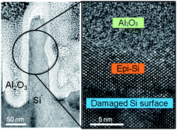
Metal-assisted chemical etching is useful and cost-efficient for nanostructuring the surface of crystalline silicon solar cells. We have found that the nanoscale epitaxy of silicon occurs, upon subsequent annealing, at the Al2O3/Si interface amorphized by metal-assisted etching. Since this epitaxial growth penetrates into the pre-formed Al2O3 film, the bonding nature at the newly formed interfaces (by the regrown epitaxy) is deteriorated, resulting in a poor performance of Al2O3 passivation. Compared to the conventional hydrogen (H–) passivation, hydroxyl functionalization by oxygen plasma treatment was more effective as the wafer became thinner. For ultrathin (∼50 μm) wafers, ∼30% depression in surface recombination velocity led to the improvement of ∼15.6% in the short circuit current. The effectiveness of hydroxyl passivation validated by ultrathin wafers would be beneficial for further reducing the wafer cost of nanostructured silicon solar cells.


In recent years, nanostructured surfaces of silicon have been extensively explored due to their excellent ability to absorb incident solar light via light-trapping features.1,2 Metal-assisted chemical etching (MaCE) is especially useful for cost-efficient solar cell applications based upon nanostructured crystalline silicon (c-Si) and has attracted much attention. Other methods for nanostructuring Si surfaces, such as vapor–liquid–solid (VLS) growth and reactive ion etching (RIE), have also been investigated.3,4 Surface nanostructuring by MaCE at room temperature is known to form an amorphous oxide on a roughly etched c-Si surface.5–8 Metal impurities are also present inside the oxide layer. These surface oxides need to be removed to protect the photovoltaic performance from contamination by metal impurities and to allow for reasonable Ohmic contact formation between the metal electrode and the substrate. Typically, fluorine-containing wet solutions, such as HF and NH4F, are capable of washing out the silicon oxide by forming soluble SiFx while terminating the Si surface with hydrogen.

Hydrogen-terminated surfaces are chemically inert due to the lower polarity of Si–H bonds relative to Si–Si bonds.9,10 Previous studies have also reported that the passivation effectiveness of H– termination is determined by the polarization state of the Si–Si back bonds, which underlie the topmost Si layer, as well as the atomic smoothness of the Si surfaces.11,12 The MaCE likely exposes highly disordered crystal planes and also roughens the etched surfaces,6,13 resulting in the deterioration of the passivation performance between HF molecules and a Si surface. Since the bandgap states, such as dangling bonds at the roughened surface, are able to promote electron–hole recombination, an additional step after the HF treatment is necessary to improve the carrier collection efficiency of nanostructured c-Si solar cells. Atomic layer deposition (ALD) of Al2O3 is known to improve the passivation characteristics on a planar (or a moderate) surface morphology, in which the significance of surface hydroxyl groups in reaction with trimethylaluminum [TMA, Al(CH3)3] source was previously denoted.14 Post-annealing was also necessary for making the interfacial oxides while decreasing the interfacial defect density.15 However, this effectiveness by ALD is reduced for nanostructured surface morphologies.16–18

Here, we show that epitaxial regrowth of silicon was found at Al2O3/Si interfacial regions that have been roughened by MaCE, after the silicon has undergone subsequent annealing. Since epitaxial silicon (epi-Si) normally grows into the Al2O3 film, the pristine Al2O3 morphology (pre-formed by ALD) and the bonding nature at the newly formed interfaces by the regrown epi-Si are degraded. Interestingly, oxygen plasma-treated hydrogen passivation (OPH) was found to be more effective than the conventional hydrogen passivation (CH) for preventing surface recombination at the rough Al2O3/Si interfaces that are formed by the regrown epi-Si. Raman spectroscopy and photo-induced carrier lifetime measurements confirmed a decrease in the number of Si dangling bonds as well as an improvement in the interfacial quality between Al2O3 and Si.

High-resolution transmission electron microscopy (HRTEM) atomically resolved the interfacial regions of Al2O3/Si (Fig. 1). Compared to the non-etched, planar interface (shown in panel a), a rough interface that has been nanostructured by MaCE (panels b and c) clearly demonstrates the presence of regrown epi-Si (region II) in between the Al2O3 and silicon bulk (region I). Since the roughly interfaced sample was extracted from the vertical sidewall of nanostructures etched by MaCE, the growth direction of epi-Si was observed to be {110}. The electron diffraction pattern (inset of panel c) indicates a (111)-plane-spacing (i.e., d111) of 0.316 nm in the first few Si atomic rows. Alternatively, the diffraction pattern of the planar sample corresponds to a d100 of 0.54 nm (see inset of panel a). Moreover, the faint ring patterns, which reflect a semi-crystalline morphology, are also included in the inset of panel c because the structure at the surface of the silicon was destructed during the MaCE step. In fact, the intensity plot (panel d) of the image contrast (along the white line denoted AB in panel c), confirms the presence of a structurally destructed area (region I) in between the regrown epi-Si (region II) and the non-destructed Si bulk.


image file: c5ra03775a-f1.tif
Fig. 1 Cross-sectional TEM images showing the interfaces of (a) Al2O3/planar Si and (b and c) Al2O3/NS (nanostructure) Si. Panel c is a highly magnified view of the region circled in black in panel b. Scale bars are 5 nm for panels a and c, and 50 nm for panel b, respectively. In the insets, electron diffraction patterns are taken along the [110] zone-axis. (d) The intensity plot of image contrast along the vertical white line (denoted AB in panel c). (e) EEL spectra spatially resolved with a spectral interval depth of 0.76 nm.

Electron energy loss spectroscopy (EELS) results, shown in panel e, spatially resolves the chemical information of each interfacial region with a spectral interval depth of 0.76 nm. The energy-loss near-edge structure (ELNES) in an EEL spectrum is sensitive to the valence and the coordination of specific elements.19 In our work, the Al coordination and the interfacial bonding structure of Al2O3/Si are investigated using the Al L23 and Si L23 ELNESs (Fig. 1e). Peak doubling is observed at 77.5 and 79.1 eV in the Al ELNES, reflecting the tetrahedrally (T) and octahedrally (O) coordinated aluminum, respectively.20 These peaks are caused by the Al2O3 film, but disappear close to the substrate (region I), suggesting a destructed silicon lattice. The coexistence of Si L23 (∼100 eV) along with the Al L23 edges throughout the region II clearly indicates that the epitaxial silicon penetrated into the Al2O3 film by destructing the pristine Al2O3 morphology, which is supported by high resolution TEM images before and after post-annealing. (See ESI), Fig. S2). Note that the Si L23 edge slightly shifts ∼0.7 eV (denoted by horizontal arrows) in region II. This indicates the change in bonding nature of silicon, i.e., silicates (not SiO2) containing SiO4 tetrahedra.21 This change is caused by the thin defective oxide newly formed underneath the Al2O3, which has been destructed by epi-Si. Generally, ultrathin (∼0.5 nm) SiOx is known to form at the interface between ALD Al2O3 and planar Si upon post-annealing of ALD Al2O3.22 We have also observed the presence of the interfacial SiOx layer for the planar sample (Fig. 1a). Given nanostructured Si (Fig. 1c), however, the observation of the SiOx interlayer became more difficult because of the formation of defective oxides (silicates) by epitaxial regrowth.

The presence of a thin silicate layer in region II was also confirmed by Raman spectroscopy. Fig. 2 shows the Raman spectra of planar and NS Si, which were passivated by ∼15 nm thin Al2O3 films. The overall Raman intensity in NS morphologies normally increases because the surface area increased by nanostructuring causes to enhance the inelastic scattering of silicon phonons.23 The Raman peak observed at 437 cm−1 indicates the presence of Si–O–Si bending mode.24,25 Moreover, the spectral intensities between 940 and 990 cm−1 are much more evident compared to those in planar Si. This indicates the stretching motions of symmetric silicon–oxygen bonds in silicate units containing two non-bridging oxygen ([double bond, length as m-dash]SiO2).26 These features imply that the original bonding network (O[double bond, length as m-dash]Si[double bond, length as m-dash]O) of tetrahedrally coordinated oxygen has been destroyed in the defective oxide (silicate) via strained (bended) Si–O bonds and broken units of [double bond, length as m-dash]SiO2. As a result, the increased number of Si dangling bonds (DB) at the defective oxide leads to the mid-gap states, which act as a dominant source of surface recombination.


image file: c5ra03775a-f2.tif
Fig. 2 Raman spectra comparing the planar (blue) and NS (red) silicon passivated by Al2O3.

We have also conducted our oxygen plasma treatment prior to conventional H-termination (with an HF solution) because this pre-treatment has been shown to form an ultrathin (≤2 nm) SiO2 layer. This layer serves as an acceptable electric contact pad and matches with a subsequent ALD of Al2O3.27,28 The inset of Fig. 3b compares the impact of oxygen plasma-pretreatment on the optical phonon mode around 520 cm−1 for the NS samples with a nanostructure height of 500 nm. Note that a slight shift of ∼0.6 cm−1 to a higher energy was observed in the oxygen plasma-pretreated samples. Since the adsorbed oxygen ions readily convert into the OH– groups in air exposure, the hydroxyl functionalized surface is more energetically favorable than the conventional H-termination for inducing the Al–O–Si bonds during the initial stage of the Al2O3 ALD process.14 An increased amount of O–Si bonds at the oxygen plasma-pretreated surface was verified by a high-energy shift of ∼0.6 cm−1 in optical phonon mode of silicon; the inelastic interaction between the incident beam and Si atoms decreased due to the attenuated concentration of the electron charges around the silicon atoms bonded to oxygen atoms. Compared to the electronegativity of hydrogen (EN ∼ 2.1), the high EN of oxygen (∼3.5) likely induces strong dipole polarization during bonding with silicon (EN ∼ 1.8). This causes a decrease in the inelastic scattering of electrons in silicon with the incident beam. As a result, the optical phonon mode of silicon is likely to shift to higher energy. In general, the position of a bulk phonon mode (520 cm−1) would not be perturbed by modifying surface treatments. In our case, however, the increased amount of O–Si bonds affected by the OPH causes a slight shift of ∼0.6 cm−1 to a higher energy. This feature was also reported in previous work,23 in which the Raman peak at 520 cm−1 was shifted and broadened by surface oxidization of Si nanorods prepared by metal-assisted chemical etching.


image file: c5ra03775a-f3.tif
Fig. 3 (a) FTIR spectra comparing the CH (black) and OPH (blue) Si nanostructures (NS). Conventional hydrogen passivation (CH) was prepared by HF dipping (60 s), and the oxygen plasma-pretreated hydrogen passivation (OPH) was prepared by the O2 plasma prior to HF dipping (20 s). (b) Surface recombination velocity (SRV, cm s−1) is plotted as a function of nanostructure heights, in which the CH and OPH samples are compared. The SRV improvement ratio (red) by oxygen plasma is extracted via the relationship of [(SRVCH − SRVOPH)/SRVCH], according to the NS heights. In the inset, the Raman spectra for the Si phonon mode of CH (black) and OPH (blue) are taken at a NS height of 500 nm.

The increased number of the OH– groups has also been observed using the FTIR (Fourier transform infrared spectroscopy) result performed prior to the ALD process (see Fig. 3a). The FTIR data compared the two absorption peaks at 800 cm−1 (Si–OH) and 1100 cm−1 (Si–O–Si) stretching modes, in which stronger absorptions were recorded upon the HF-etched samples after O2 plasma.11

MaCE is known to amorphize the surface by the physicochemical damage that occurs during the electroless etching used for nanostructuring.5 Since the formation of an amorphous phase causes the silicon atoms to be more weakly bonded compared to those in a crystalline phase (2.3 eV), the surface amorphous layer formed by etching would be an effective source of Si atoms for epitaxial recrystallization. As a result, the presence of OH– groups (by O2 plasma treatment) would likely reduce Si diffusion due to the higher binding energy of Si–O bonds (∼452 kJ mol−1) compared to Si–H bonds (∼393 kJ mol−1). The surface improvement by OPH leads to the saturation behavior of the surface recombination velocities (SRV) as the nanostructure height increases (Fig. 3b). This is in direct contrast to the H-terminated NS sample. The SRV improvement (right y-axis) by OPH was estimated via the relationship of [(SRVCH − SRVOPH)/SRVCH], which is estimated to increase from 22 to 60% as the NS heights increase from 300 to 800 nm (for each cross-sectional morphology, see ESI, Fig. S3).

The effectiveness of OPH needs to be further tested as the wafer thickness is decreased from 200 to 50 μm. The optimal balance between optical and electrical aspects of nanostructured silicon solar cells was evaluated using a figure-of-merit (ΔJsc/Aave), where the ΔJsc is the electrical gain in Jsc that is caused by OPH relative to H-termination and the Aave is the light absorption (λ = 400–1100 nm) at different wafer thicknesses (see ESI, Fig. S4). Since the light absorption decreases with decreasing wafer thickness, the comparison between ΔJsc/Aave and ΔJsc is indicative of practical effectiveness of OPH on ultrathin NS c-Si solar cells. The ΔJsc (right y-axis) values increase from 6.6 to 11.7% as the wafer thickness decreases from 200 to 50 μm (Fig. 4a). Despite the suppressed light absorption at longer wavelengths as the wafer becomes thinner, we discovered that the low-energy photons transmitted without absorption in thinner samples are more likely to generate charge carriers via back-reflection from the Al electrode; back-reflected photons are more readily available to approach the p–n junction with a thinner absorber. The figure-of-merit (ΔJsc/Aave), which recognizes that the light absorption decreases with wafer-thinning, more clearly describes the efficient collection of charge carriers in the hydroxyl functionalized thinner wafers. This figure of merit shows an improvement of ∼15.6% at 50 μm thick wafer, while the improvement recorded by ΔJsc only is ∼11.7%. The enhanced passivation performance increased Jsc (+2.4 mA cm−2) as well as Voc (+13 mV) (Fig. 4b and Table 1). An increase of carrier diffusion length/wafer thickness (L/W in the inset of Fig. 4a) suppressed the reverse saturation current in c-Si solar cells,29 resulting in an increase of Voc. The improved blue-response of the internal quantum efficiency (IQE) in wavelengths shorter than 500 nm also denotes the fact that the high-energy photons are more effectively absorbed into the hydroxyl functionalized, thin wafer compared to the conventional H-terminated wafer. As a result, the cell efficiency increased from 6.88% to 7.90% in a 50 μm-thick c-Si solar cell without any antireflection coating and selective emitter processes.


image file: c5ra03775a-f4.tif
Fig. 4 (a) Plots comparing the ΔJsc/Aave vs. ΔJsc, in which the ΔJsc denotes the Jsc gain that occurs when the OPH is used instead of H-termination. Aave is the amount of light absorptions (λ = 400–1100 nm) at different wafer thicknesses. Inset shows the relevance of carrier diffusion length (L) and wafer thicknesses (W). (b) JV curves for CH (red) and OPH (black) NS solar cells using 50 μm thick substrates. In the inset, blue responses (λ = 400–650 nm) of the internal quantum efficiency (IQE) are compared between the CH and OPH.
Table 1 Photovoltaic performances of CH and OPH NS solar cells using 50 μm thin substrates
  Voc [mV] Jsc [mA cm−2] FF [%] CE [%]
CH + Al2O3 522 20.4 64.6 6.88
OPH + Al2O3 535 22.8 64.8 7.90


In summary, we demonstrated for the first time that the nanoscale epitaxial regrowth of silicon occurs during the subsequent annealing at surfaces that have been damaged by electroless etching during surface nanostructuring. Since the growth of epitaxial silicon normally penetrates into the Al2O3 film by destructing the pre-formed Al2O3 morphology, the surface bonding structure of the newly formed interfaces was determined to be much poorer relative to the conventional c-Si surface. Compared to conventional hydrogen passivation, hydroxyl functionalization by oxygen plasma pretreatment was more effective. This effectiveness was caused by a 22–60% improvement in surface recombination velocity, which depended upon the height of the nanostructure. This notable improvement by oxygen plasma originated from the saturation behavior of the surface recombination velocities, which degraded with increasing nanostructure height. To realize a thin (≤50 μm) crystalline silicon solar cell based on cost-efficient surface nanostructuring, the utilization of an oxygen plasma-treatment might be necessary in order to retain photovoltaic performances while decreasing consumption of high-purity silicon.

Acknowledgements

This work was supported by the New & Renewable Energy of the Korea Institute of Energy Technology Evaluation and Planning (KETEP) grant (no. 20123010010160) funded by the Korea government Ministry of Trade, Industry and Energy. This work was also supported by the National Research Foundation of Korea (NRF) grant funded by the Korea government (MSIP) (no. 2011-0028604). RBW is grateful for funding by the BMBF project Strutkursolar.

Notes and references

  1. B. Z. Tian, X. L. Zheng, T. J. Kempa, Y. Fang, N. F. Yu, G. H. Yu, J. L. Huang and C. M. Lieber, Nature, 2007, 449, 885–889 CrossRef CAS PubMed.
  2. E. C. Garnett and P. D. Yang, J. Am. Chem. Soc., 2008, 130, 9224–9225 CrossRef CAS PubMed.
  3. W. I. Park, G. Zheng, X. Jiang, B. Tian and C. M. Lieber, Nano Lett., 2008, 8, 3004–3009 CrossRef CAS PubMed.
  4. H. Park, D. Shin, G. Kang, S. Baek, K. Kim and W. J. Padilla, Adv. Mater., 2011, 23, 5796–5800 CrossRef CAS PubMed.
  5. W. Chern, K. Hsu, I. S. Chun, B. P. D. Azeredo, N. Ahmed, K. H. Kim, J. M. Zuo, N. Fang and X. Li, Nano Lett., 2010, 10, 1582–1588 CrossRef CAS PubMed.
  6. J. Kim, H. Han, Y.-H. Kim, S.-H. Choi, J.-C. Kim and W. Lee, ACS Nano, 2011, 5, 3222–3229 CrossRef CAS PubMed.
  7. K.-Q. Peng, J. Hu, Y. Yan, Y. Wu, H. Fang, Y. Xu, S. T. Lee and J. Zhu, Adv. Funct. Mater., 2006, 16, 387–394 CrossRef CAS PubMed.
  8. K.-Q. Peng, Y.-J. Yan, S.-P. Gao and J. Zhu, Adv. Mater., 2000, 14, 1164–1167 CrossRef.
  9. M. Niwano, J. Kageyama, K. Kurita, K. Kinashi, I. Takahashi and N. Miyamoto, J. Appl. Phys., 1994, 76, 2157–2163 CrossRef CAS PubMed.
  10. H. Angermann, Th. Dittrich and H. Flietner, Appl. Phys. A, 1994, 59, 193–197 CrossRef.
  11. D. J. Michalack, S. R. Amy, D. Aureau, M. Dai, A. Esteve and Y. J. Chabal, Nat. Mater., 2010, 9, 266–271 Search PubMed.
  12. R. Q. Zhang, Y. L. Zhao and B. K. Teo, Phys. Rev. B: Condens. Matter Mater. Phys., 2004, 69, 125319 CrossRef.
  13. J.-W. Song, J.-Y. Jung, H.-D. Um, X. Li, M.-J. Park, Y.-H. Nam, S.-M. Shin, T. J. Park, R. B. Wehspohn and J.-H. Lee, Adv. Mater. Interfaces, 2014, 1, 1400010 Search PubMed.
  14. V. Naumann, M. Otto, R. B. Wehrspohn and C. Hagendorf, J. Vac. Sci. Technol., A, 2012, 30, 04D106 Search PubMed.
  15. B. Hoex, J. J. H. Gielis, M. C. M. van de Sanden and W. M. M. Kessels, J. Appl. Phys., 2008, 104, 113703 CrossRef PubMed.
  16. B. Dou, R. Jia, Y. Sun, H. Li, C. Chen, Z. Jin and X. Liu, J. Appl. Phys., 2013, 114, 174301 CrossRef PubMed.
  17. W. C. Wang, C.-W. Lin, H.-J. Chen, C.-W. Chang, J.-J. Huang, M.-J. Yang, B. Tjahjono, J.-J. Huang, W.-C. Hsu and M.-J. Chen, ACS Appl. Mater. Interfaces, 2013, 5, 9752–9759 CAS.
  18. Z. Huang, S. Zhong, X. Hua, X. Lin, X. Kong, N. Dai and W. Shen, Prog. Photovoltaics, 2014 DOI:10.1002/pip. 2506.
  19. Y. Matsui, T. Nabatame, T. Yasuda, T. Mizoguchi, I. Tanaka, A. Toriumi and K. Kimoto, Appl. Phys. Lett., 2003, 83, 4306–4308 CrossRef PubMed.
  20. I. Tanaka, T. Mizoguchi, T. Sekine, H. He, K. Kimoto, T. Kobayashi and S.-D. Mo, Appl. Phys. Lett., 2001, 78, 2134–2136 CrossRef CAS PubMed.
  21. R. F. Egerton, Electron Energy-Loss Spectroscopy in the Electron Microscope, Plenum Press, New York, USA, 1996 Search PubMed.
  22. B. Hoex, S. B. S. Heil, E. Langereis, M. C. M. van de Sanden and W. M. M. Kessels, Appl. Phys. Lett., 2006, 89, 042112 CrossRef PubMed.
  23. G.-R. Lin, Y.-H. Lin, Y.-H. Pai and F.-S. Meng, Opt. Express, 2011, 19, 597–605 CrossRef CAS PubMed.
  24. K. J. Kingma and R. J. Hemley, Am. Mineral., 1994, 79, 269–273 CAS.
  25. P. Borowicz, A. Taube, W. Rzodkiewicz, M. Latek and S. Gieraltowska, Sci. World J., 2013, 2013, 208081 CAS.
  26. P. Mcmillan, Am. Mineral., 1984, 69, 622–644 CAS.
  27. E. R. Cleveland, L. B. Ruppalt, B. R. Bennett and S. M. Prokes, Appl. Surf. Sci., 2013, 277, 167–175 CrossRef CAS PubMed.
  28. M. Fukasawa, Y. Nakakubo, A. Matsuda, Y. Takao, K. Eriguchi, K. Ono, M. Minami, F. Uesawa and T. Tatsumi, J. Vac. Sci. Technol., A, 2011, 29, 041301 Search PubMed.
  29. C. J. J. Tool, A. R. Burgers, P. Manshanden, A. W. Weeber and B. H. M. van Straaten, Prog. Photovoltaics, 2002, 10, 279–291 CAS.

Footnote

Electronic supplementary information (ESI) available: Experimental methods, FTIR absorption data, cross-sectional FESEM images of varied heights of NS Si, and light absorption of NS Si arrays (height = 500 nm) with various wafer thicknesses. See DOI: 10.1039/c5ra03775a

This journal is © The Royal Society of Chemistry 2015