Chemical vapour deposition of Ir-based coatings: chemistry, processes and applications

V. Yu. Vasilyev ab, N. B. Morozova *a, T. V. Basova *ac, I. K. Igumenov a and A. Hassan d
aNikolaev Institute of Inorganic Chemistry, Siberian Branch of the Russian Academy of Sciences, Prosp. Academika Lavrentieva 3, 630090, Novosibirsk, Russian Federation. E-mail: mor@niic.nsc.ru; basova@niic.nsc.ru
bNovosibirsk State Technical University, Prosp. K Marksa 20, 630073 Novosibirsk, Russian Federation
cNovosibirsk State University, Pirogova Str.2, 630090, Novosibirsk, Russian Federation
dMaterials and Engineering Research Institute, Sheffield Hallam University, Sheffield S1 1WB, UK

Received 2nd March 2015 , Accepted 27th March 2015

First published on 27th March 2015


Abstract

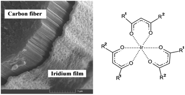
Chemical and materials science aspects of iridium-containing thin film formation by Chemical Vapor Deposition (CVD) methods for modern high-precision technology applications are considered. Chemical approaches to the synthesis of the main precursors used in CVD techniques, thin film growth processes and mechanisms as well as the main structure, composition and properties of iridium-containing thin films are analyzed, and modern thin film application examples are outlined. Numerical characterization of iridium-based thin film growth in 3D objects is presented.


image file: c5ra03566j-p1.tif

V. Yu. Vasilyev

Vladislav Yu. Vasilyev received his Ph.D. and D.Sc. degrees in chemistry from Russian Academy of Sciences in 1990 and 2002, respectively. Having totally over 35 years of experience in microelectronics technology, he worked as a researcher at R&Ds of Novosibirsk Semiconductor Devices Manufacturing (Russia) and Chartered Semiconductor (Singapore). He studied ruthenium thin film ALD under South Korea Governmental Brain Pool Program. Currently he is a Deputy General Director of IC design center SibIS LLC (Russia) and a Professor at the Novosibirsk State Technical University. Main research interests are thin film chemical vapor deposition, growth kinetics, reaction mechanisms, thin film applications.

image file: c5ra03566j-p2.tif

N. B. Morozova

Natalya B. Morozova received her Ph.D. and D.Sc. degrees in chemistry from Russian Academy of Sciences in 1996 and 2009, respectively. Now she has position of the head of laboratory at the Nikolaev Institute of Siberian Branch of RAS, Novosibirsk. She has more than 20 years of experience in chemistry of volatile organometallic compounds, precursors for MOCVD technique, chemical synthesis of a wide range of materials from volatile coordination and metal–organic compounds to high temperature stable, solid state films and in applications including film growth by MOCVD.

image file: c5ra03566j-p3.tif

T. V. Basova

Tamara Basova received her PhD (1999) and DSc (2011) in Physical Chemistry from Nikolaev Institute of Inorganic Chemistry, Novosibirsk, Russia. Now she is a leading researcher in the institute. Her research interests are mainly directed towards the synthesis and characterization of various metal phthalocyanines and other molecular compounds, and the investigation of the structure, sensor and electrical properties of oriented molecular films.

image file: c5ra03566j-p4.tif

I. K. Igumenov

Prof. Igor Igumenov was born in Novosibirsk, Russia Federation, in 1944. At present time he is a leading researcher in the Nikolaev Institute of Inorganic Chemistry of Russian Academy of Sciences. His research interests comprise different aspects of physical chemistry of volatile metal complexes with organic ligands including thermodynamics of vaporization and mechanisms of heterogeneous thermal conversions, design of MOCVD precursors, study of growth of nanostructured films upon MOCVD.

image file: c5ra03566j-p5.tif

A. Hassan

Aseel Hassan BSc, MSc, PhD in Physics, is a Senior Lecturer at the Faculty of Arts, Computing Engineering and Sciences of Sheffield Hallam University, UK. He carries out his research within the Materials and Engineering Research Institute and his interest lies in thin film technology mainly for application in chemical and biosensing. He uses optical techniques such as surface plasmon resonance and spectroscopic ellipsometry, as well as quartz crystal microbalance detection techniques, employing organic films as the sensing layers. Dr Hassan also specialises in physical electronics and focuses mainly on photovoltaic research and development.


1 Introduction

Layered semiconductor, dielectric and conductive materials (commonly named “coatings” or “thin films”) formed on the surface of solid substrates are widely used in modern high-precision technologies. These thin film materials have found a variety of technological applications in electronics, micro-electro mechanical system technology, nanoelectronics, power electronics, medicine, and so on. Conventional methods of thin film deposition include for instance, physical vapor deposition from the gas phase (PVD), thermal or electron beam evaporation in high vacuum followed by condensation, cathode spraying, magnetron sputtering, and electrolysis of salt melts. During recent decades, various options of Chemical Vapor Deposition (CVD) have become the most widespread methods for the deposition of thin film materials.

Among the other attractive metals for modern high-precision technologies, platinum group metals have attracted increasing attention of scientific and technical communities due to their unique physical and chemical properties. Generally, these metals have high melting temperatures, high resistance towards oxidation and good electrical conductivity, biological compatibility and radiopacity. In some cases this allows to consider these metals as ideal electrode material and barrier material for future microelectronic devices and manufacturing of medical equipment such as electrodes for pacemakers. Furthermore, some of these metals like ruthenium and iridium have low resistivity oxides that make them suitable in IC device technology with several oxidation processes used.1,2

Metal iridium in particular exhibits a rare combination of chemical and physical properties. It is stable against various chemical reactions. In its metal form, iridium is insoluble in mineral acids (including aqua regia and fluoric acid), does not interact at high temperatures with the melts of other metals or silicates, does not form carbides when in contact with carbon, and possesses high resistance against oxidation. Iridium also has a high melting point (2443 °C), and it is the only metal possessing unique mechanical characteristics in air at temperatures above 1600 °C. Ir-based thin film coatings have found a broad range of applications which include their use in protecting refractory materials in high-temperature processes of glass melting or crystal growth, in rocket technologies for the protection of combustion chambers in engines and turbine blades, in electrochemical processes to protect electrodes, in various areas of catalysis, in developing power optics elements for high-power lasers, for film thermocouples manufacturing, and as electrical contacts.

Electro-chemical deposition, magnetron sputtering, and metal–organic chemical vapor deposition (MOCVD) processes have been successfully used for the deposition of Ir coatings.3–5 CVD is one of the most dynamically developing methods of forming metal layers for different purposes. Compared with the coatings prepared by electrodeposition and magnetron sputtering, the coatings deposited by MOCVD have smaller grain size and different grain structure.6,7 A distinguishing feature of CVD method is the efficient control of the process parameters and therefore the required characteristics of the resulting layers and structures are crystallite size, thickness of the coating, and its structure and morphology.

Until recently, only a few attempts have been made to review accumulated data on CVD platinum metals films (Ru, Rh, Pd, Os, Ir, Pt).8–13 Up to date, a recent review on ruthenium film deposition5 seems to be the only attempt to summarize a wide range of information regarding thin films of selected noble metal materials from precursor chemistry to film growth, structure, properties, and applications. This allows obtaining a comprehensive vision of CVD deposited ruthenium thin films. In contrast to ruthenium CVD thin films, which are mostly considered for use in microelectronic technology and nano-technology applications, Ir-based films demonstrated a much wider range of technological applications which have been discussed in several reviews.14–16

The success of CVD strongly depends on the properties of a suitable precursor which should have high volatility, thermal stability and ability to clean decomposition. A comprehensive review describing a variety of iridium volatile compounds have been reported in 2003.5 Most recent studies have been focused on characterization of the latest iridium precursors and CVD processes, as well as deposited coatings. Usually these reports present only a brief description of experimental procedures and therefore we believe that there is relatively limited information since a correct examination and comparison of the CVD features are far from complete. In this review we analyze the results of the most representative publications reported in the last few years. It is an attempt to summarize materials related to CVD of Ir-based thin film coatings (preferably on iridium metal thin films), including chemistry of precursors, deposition processes and mechanisms of thin film growth, film characterization, and basic applications of Ir-based thin films.

2 Brief thin film deposition review

2.1 General aspects

Semiconductor, dielectric and metallic thin film coatings dedicated for the use in high-precision technologies are fabricated mostly using either PVD technique (sputtering from appropriate targets) or various versions of CVD technique. Generally, the PVD technique is excellent choice for metallic (including platinum group metals) thin film deposition.17,18 Particularly, a number of studies of sputtered iridium thin films have been published.4,19–23 Obvious advantages of sputtered thin films are simplicity of the method and material purity as well as capability to form metal silicides being deposited on silicon and thermally annealed. It seems that only sputtered films can serve as a reference for comparison of CVD thin film composition and properties.

However, PVD methods have limited use for fabrication of conformal thin films in complex 3D structures (in a simplest case defined in percent as the ratio of thin film thickness on the structure side-wall surface to that in the top of the structure surface). In this case the narrow gaps, for instance, between functional units of modern integrated circuits (IC), remain unfilled and undesired voids inside IC devices can appear. The requirement for conformality of coatings of the structures with high aspect ratios is of particular importance for modern microelectronics technology that was analyzed quantitatively.24,25

CVD methods have been used to fabricate “substrate-thin film” structures since the mid-1960s.26 In a CVD process, the growth of a thin film coating on the surface of a sample heated to the desired temperature is the result of irreversible reactions of initially gaseous or vaporized chemical compounds. Thin films are synthesized using both CVD flow reactors, which operate at atmospheric, reduced and low pressures. A CVD process can occur either as a pyrolysis of vapors of single organometallic compounds, or in the presence of a second reactant and, in particular, involves the formation of intermediates of the reaction between reactants in the vapor phase. The latter case means that vapor-phase mixtures of the precursors and some other compounds (for instance, oxidants, ammonia, etc.) in the presence of various carrier gases are supplied to the reactor by a pressure drop in the carrier gas stream or as a result of the evacuation of the system with a vacuum pump. One of the most important features of CVD processes is the possibility to grow thin film coatings of variable thickness (from a few hundredths of a micrometer to a few micrometers) at relatively low temperatures. The film deposition temperature can also be reduced by an additional (non-thermal) activation of the vapor phase using a high-frequency discharge, photochemically or by using laser irradiation.27

Wide use of CVD methods in basic research and large-scale production is due to the fact that they require relatively simple equipment, they are safe and manufacturable, and they provide high quality thin-film coatings fabricated under the pre-optimized CVD conditions. Chemical vapor-phase deposition methods provide significantly better thin film conformality on complicated IC device structures and they are more promising for application to modern complex 3D systems. For instance, thin film CVD processes have become basic technological processes in microelectronics.17,27–31 At present, their proportion in the overall integrated circuits (IC) fabrication cycle is continuously increasing as the IC devices and methods of multilayer structures for ICs become more and more complicated.

The considerable interest in the CVD processes is reflected in a continuous stream of publications, most of which describe the operation regimes, reactors and the properties of the films obtained. The properties of the films have been studied to different extents. To date, CVD of dielectrics (silicon dioxide, silicon nitride, glasses, porous materials, etc.) are well-developed production processes. The history of CVD metallic materials is shorter, because PVD methods have been actively used for excellent thin film deposition on substrates with flat or relatively simple stepped surfaces. CVD and MOCVD have been used for film deposition because of the superior step coverage on 3D structures compared to the conventional PVD processes.24,31

Recently, in connection with complication of the shape of modern electronic devices and the need for preparation of thin conformal coatings, a CVD technique with pulsed consecutive feed of reactants and purge gas (below P-CVD method) has been developing intensively.29,32–35 Here, deposition occurs in cyclic manner; the overall deposition cycle using two initial reactants involves four consecutive pulses of precursor vapors, purge gas, second reactant and purge gas again. In some cases, more complicated designs are used, which involve intermediate evacuation of the reaction chamber.32–34 A number of CVD reaction systems allow the films to grow in the so-called atomic layer deposition (ALD) regime, provided optimized temperature conditions, cyclic regime, appropriately chosen reactant doses and particular temperature ranges. Usually, ALD processes can be practically implemented using precursors that are prone to chemical interaction with the substrate (chemisorption). The limiting stage of the overall ALD process that is entirely localized on the surface of a sample is the interaction of the chemisorbed precursor with the second reactant deposited on the surface from the vapor phase provided that all adsorption sites are filled to achieve self-limiting growth of the film.28 With this mechanism, film deposition in the ALD regime should provide layer-by-layer growth and, as a consequence, almost 100% degree of conformality of the deposited films on the inner surfaces of complex-shape 3D structures. General data regarding ALD thin film synthesis can be found elsewhere,28 and some differences in determination of P-CVD and ALD have been discussed recently in a review.29 Particularly, according to the latter, the overall process is termed P-CVD if self-limiting behavior cannot be achieved, even in cases where ALD reactivity is accompanied by a minor parasitic CVD process.

2.2 Equipment and methodology

Generally, more or less information regarding typical equipment and methodology can be found in any summary about CVD thin film.26–28,30,31,34 Up to date the most comprehensive vision of CVD equipment and methodology in conjunction with these film processes, deposition kinetics and thin film properties seem to be a review written by Vasilyev and Repinsky30 as well as a recent monograph on CVD thin films in electronics by Vasilyev.31 The latter covers a wide variety of aspects and tries to establish a systematic view on the different deposition processes (including various CVD, MOCVD, P-CVD, ALD), thin film properties and application of thin films with respect to the electronic applications.

It is also necessary to point out that there were some attempts to modify the CVD equipment with analytical tools, for instance, mass-spectrometry units. This allowed the study of thin film deposition processes in situ and to make some proposals regarding possible reaction mechanisms.35–38 All these attempts are undoubtedly important for the future of in-depth studies of thin film production on nano-level.39,40

2.3 Precursors

During recent decades, CVD has become the most widespread method for depositing platinum group thin film coatings. Chemistry of precursors plays the key role in these processes because deposition parameters and the design of MOCVD tools are determined by the set of physicochemical characteristics of the compounds used. The major requirements to MOCVD precursors are volatility (ability to pass into the gas phase without decomposition at moderate temperatures (below 250 °C), and thermal stability in the condensed and gas phases. Normally, various classes of volatile coordination and organometallic compounds are used as MOCVD precursors. The active development of the chemistry of these compounds is connected with the great diversity of properties depending on the chemical composition and structure of complexes and, as a consequence, with the possibility of their practical application. Some good examples of general reviews on precursor chemistry and its link to the CVD and ALD processes and film growth mechanisms can be found elsewhere.41–46

The thermal properties of the compounds in the condensed and gas phases, including thermal stability in the solid phase, vapor pressure and the routes of precursor vapor decomposition with (or without) reaction additives, determine the specific composition of the material of coating, its structure and morphology for the realization of MOCVD processes. The major requirements to the precursors have been formulated as follows:16

(1) Thermal stability of the precursor in the condensed state at vaporization temperature;

(2) high vapor pressure (volatility) of precursor;

(3) stability in the gas phase at vaporization temperature;

(4) decomposition of precursor vapor with the formation of the material of coating and gaseous products only;

(5) moderate temperature of film deposition, that is, not high threshold of precursor vapor stability;

(6) inertness of precursor vapor and gaseous decomposition products to the substrate material;

(7) non-toxic character, stability in the air, storage stability, high yield from synthesis, availability of starting reagents.

Similar set of requirements has been formulated by Dussarrat.46 The main requirements for the chemical precursors used in ALD are that they:

(1) must be volatile (preferably at room temperature or at least at reasonable delivery temperatures, around 120 °C, or almost always below 200 °C). A convenient criterion is to set a minimum vapor pressure of 0.1 torr at ∼120 °C, but it might be amended depending on the precursor stability;

(2) should not self-decompose neither at delivery conditions nor at the process temperatures so as to confine a chemisorption mechanism limited to co-reactant reactive sites. Consequently, one monolayer per cycle can grow at most (a monolayer is typically ∼0.24–0.3 nm). In practice, only a fraction of a monolayer is deposited. One third of monolayer is typically observed (e.g. 0.08–0.1 nm per cycle), although the growth can be sometimes much more limited;

(3) should be sufficiently reactive to the surface so that chemisorption can occur effectively. For example, methylsilanes may not react to the surface, and are then unsuitable for ALD if they do not contain bonds like Si–Cl and Si–N then can dissociate at the contact of the surfaces. Also, depending on the targeted metals some elements are hard to remove if undesired, and their presence is therefore undesirable. Carbon may be acceptable in some cases, but may lead to significant carbon incorporation in the films. This is specifically true when nitrides or pure metals are desired, as the presence of carbon impacts their electrical properties for instance;

(4) are preferably liquid. This is not compulsory, and some solid precursors are currently used in the industry, but thorough investigations of the consequences are necessary, allied with a rigorous inspection to prevent adverse situations. Multiple examples of precursor clogging in the delivery lines or at the valve are reported. Also the feed rate of a solid precursor may vary with time, as a consequence of the faster sublimation of small grains, and the change of particle morphology during prolonged heating;

(5) must be of high purity, especially when distributed in bubbling or cross-flow mode, in order to assure a constant flow rate of material in the reactor, as industrial processes using ALD technique are typically very sensitive to purity changes.

2.4 Deposition process description

Both research practice and applied use of CVD methods face the problem of describing the film growth processes, which involves the establishment of some basic functional dependences.30,31 First, it is necessary to characterize chemical kinetics of the film growth, i.e. to obtain quantitative relations between the film growth rate and a set of “input” CVD process parameters. They usually include a number of key process parameters, such as temperature (T), pressure (P), linear rate of gas stream (υ) and the ratio of the component concentrations in the vapor phase (taking into account the geometry of the CVD reactor), features of the spatial arrangement of samples in the reactor and the thermal and gas-dynamic effects in the reactor, and film nucleation effects. Usually, these are the key factors for the optimization of the film deposition process, which eventually involves achievement of a maximum film growth rate at a minimum possible film thickness mismatch (desired values lie within limits of a few percent) across the entire sample surface. The second necessary functional dependence is a relation between the chemical composition and microcomposition of the film and the input parameters of the CVD process. The third group of functional dependences includes correlations between the properties of the deposited films and the CVD conditions. It should be noted that most studies of the properties of dielectric materials were carried out using a particular deposition technique and a narrow range of parameters for the CVD processes. Finally, searching for correlations between the electrical properties of deposited materials and the CVD parameters, including the reactor type, starting compounds, deposition conditions, etc., is also an important task.

2.5 CVD production processes

In order to develop production CVD thin film processes based on sufficient characterization of the process chemistry and film properties, a number of general issues need to be solved. Taking microelectronic application of CVD processes as an illustration, it can be stated that, key features of thin film materials prepared by CVD methods consists in that their synthesis is a part of the technological process of fabrication of IC devices. Therefore, the quality and reproducibility of the properties of thin films to a great extent predetermine the performance and parameters of microelectronic devices and the nominal product yield. Main problems in the deposition of thin films on the surface of microelectronic devices fabricated on either pilot or full scale (here, the main item is usually a semiconductor wafer 100–300 mm in diameter and 450 mm in diameter in the near future, and less than 1 mm thick) are as follows:30,31

(1) search for precursors or their combinations to prepare thin films (taking into account simplicity, convenience and reproducibility of the process);

(2) search for reactor (more generally, equipment) designs to attain high performance, maximum uniformity (uniform thickness) of the deposited material and industrial safety;

(3) macrodefectness reduction of thin films (minimization of the amount of microparticles on the surface or within the deposited film);

(4) insufficient conformality of film growth within 3D structures of integrated circuits;

(5) quality control and optimization of deposition process to attain the highest degree of utilization of the precursor and reproducibility of parameters of the thin films.

In general, all problems discussed above are applicable to characterization of platinum group thin films, including Ir-based films, CVD equipment, methodology, precursors, processes, etc. Specifically for CVD thin film metal coatings it is necessary to add a couple of serious issues such as nucleation of the film in the first stage of the process and the content of carbon in the films. The first issue needs detail understanding of the sample surface properties. For instance, summary of ruthenium metal nucleation presented in a recent publication12 showed no evidence of ALD for all reviewed precursor combinations, sample materials, and process conditions. The second issue is typical for MOCVD and is the consequence of large organic groups presented in the precursors. This issue becomes more pronounced along with the precursor development and complication. To solve this, there is a need to provide precision tuning of CVD processes, for instance oxidizer/precursor ratio, in order to eliminate carbon without allowing oxide phase in metal thin films.

3 Chemistry of Ir precursors

3.1 Brief summary of previously reviewed data

Garcia and Goto summarized data related to Ir-based coatings deposited by CVD in 2003.5 Since then several new precursors have been synthesized and investigated. Table 1 provides a list of basic Ir precursors used before and after 2003 (column 3 and 4, respectively).
Table 1 Summary of basic Ir precursor groups and precursors used for Ir deposition before5 and after 2003a
# Precursor group Ir CVD precursors published before 2003 (ref. 5) IrCVD/ALD precursors (references after 2003)
a acac: [CH3–CO–CH–CO–CH3] – acetylacetonate, hfac: [CF3–CO–CH–CO–CF3] – hexafluoroacetylacetonate, thd: [C(CH3)3–CO–CH–CO–C(CH3)3] – (2,2,6,6-tetramethylheptane-3,5-dionate), COD: [C8H12] 1,5-cyclooctadiene, CHD: [C8H12] 1,3-cyclohexadiene, allyl: η3-C3H5] allyl, Cp: η3-[C5H5] cyclopentadienyl, Me: [CH3] methyl, Et: [C2H5] ethyl, [C2H4] ethylene, methoxide [CH3O], keim, hfda, amak fluorinated amino alcohol ligands.
1 Halides IrCl3, IrCl4, IrBr3, IrF6 CVD47, ALD48
2 Metal β-diketonates Ir(acac)3 CVD/P-CVD35,49–54 ALD55–62
(acac)Ir(1,5-COD), (hfac)Ir(1,5-COD), (thd)Ir(1,5-COD)
Ir(thd)3, CVD63
3 Carbonyl complexes [Ir(μ-SC(CH3)3)(CO)2]2 Ir(acac)(CO)2, P-CVD64
4 Allyl complexes Ir(allyl)3
5 Cyclooctadienyl complexes (Cp)Ir(1,5-COD), [Ir(methoxide)(1,5-COD)]2, [Ir(acetate)(1,5-COD)]2, (keim)Ir(1,5-COD), (hfda)Ir(1,5-COD), (amak)Ir(1,5-COD) CVD65,66
(EtCp)Ir(1,5-CHD) CVD67,68
(EtCp)Ir(1,5-COD) CVD69–72 ALD73–79
(MeCp)Ir(1,5-CHD) ALD80,81
6 Ethylene complexes (Cp)Ir(C2H4)2 (EtCp)Ir(C2H4)2 CVD70
7 Metal phosphines [IrCl(PF3)2]2 CVD82 IrH(PF3)4 CVD83


Among the six groups of precursors used at the earlier stages the metal β-diketonates and cyclooctadienyl complexes were the most popular ones. Note that the precursors used after 2003 (column 4 of Table 1) were utilized both in iridium CVD and ALD processes, while the precursors described before 2003 were used only in CVD processes. The ALD processes found increasing use in 2004 after the work of Aaltonen and co-workers.55

Comparative analysis of the data presented in Table 1 shows that precursors from the same groups were continued to be studied and used after 2003, namely metal β-diketonates and cyclooctadienyl complexes, however their thermal properties were improved by modifying their molecular structure. Further information regarding more promising Ir precursors (mainly β-diketonate and cyclooctadienyl derivatives) and their thermal behavior are presented in Table 2.

Table 2 Summary of basic Ir thermal CVD data5
# Precursor group Deposition temperature (K) Second reactant Deposition rate range, nm s−1
1 Halides 973–1273 Ar, H2, CO–H2O 0.07–3.33
2 Metal β-diketonates 523–873 H2, O2 0.02–0.25
3 Carbonyl complexes 423–723 H2 No data
4 Allyl complexes 373 H2, vacuum, plasma 0.0017–0.028
5 Cyclooctadienyl complexes 523–873 H2, O2 0.0027–0.25
6 Ethylene complexes Room temperature with laser H2, He No data


3.2 Synthesis and thermal properties of volatile Ir precursors

For Ir CVD precursor the halides and the following metal–organic compounds are used: heteroligand metal–organic Ir(I) compounds, heteroligand Ir(I) compounds with inorganic and organic ligands and Ir(III) complexes with organic ligands. The wide class of volatile Ir precursors is metal–organic Ir(I) compounds with general formula [XnIrYm]l, where X is Lewis bases: CO, CN, CS, P(Hal)3, As(Hal)3 (Hal – F, Cl, Br), RR1C[double bond, length as m-dash]CR2R3, CR[triple bond, length as m-dash]CR1, CR–CR1[double bond, length as m-dash]CR2–CR3 (R, R1, R2, R3 is alkyl or aryl groups), cyclohexadiene (CHD), cyclooctadiene (1,5-COD) and their derivatives; Y is i-propyl, cyclopentadienyl (Cp) cyclohexadienyl(CHD) and their derivatives (RCp and RCHD, where R = methyl, ethyl or alkyl groups); l, m, n – stoichiometric coefficients.80,84–92 Some examples of the precursors are given in Scheme 1.
image file: c5ra03566j-s1.tif
Scheme 1

Synthesis of complexes is carried out in a similar manner in several stages, in the first of which [IrXnCl]l is prepared by the action of the Lewis base on IrCl3·3H2O in a water–ethanol mixture under an inert atmosphere. The intermediates [IrXnCl] react with Yorits salts in tetrahydrofuran (THF) under an inert atmosphere. Target products are isolated by extraction and purified by chromatography. These Ir(I) compounds are crystalline solids with low melting point or liquids, depending on the nature of the Lewis base and a type of the Y ligand substituents. Therefore the compounds Ir(CHD)(EtCp) and Ir(1,5-COD)(EtCp) are liquids,80,91 and their closest analogues Ir(CHD)(MeCp) and Ir(1,5-cod)(MeCp) are solids. The yields of the compounds vary from 50 to 70%.84–86 Ir(CHD)(EtCp) is prepared with yield of 77%,91 and Ir(CHD)(MeCp) is prepared with yield of 80%.80 Ir(CO)2(Me5Cp) was synthesized by another procedure92 through preparing the intermediate [Ir(Me5Cp)Cl2]2 from H2IrCl6 and addition of Fe3(CO)12 to its solution; the yield is 70%. Crystal structures of Ir(CHD)(MeCp),80 Ir(CO)2(Me5Cp),92 and Ir(1,5-COD)(MeCp)93 were determined by XRD: the central atom geometry is flat-square, bond lengths of Ir–C(RCp) are in the intervals 2.20–2.28 Å. Thermogravimetric study of Ir(CHD)(MeCp), Ir(CHD(EtCp), Ir(1,5-COD)(MeCp), Ir(1,5-COD)(EtCp) and Ir(C2H4)(EtCp) has been carried out.70,80,91,94 All of these compounds transfer to the gaseous phase quantitatively; the volatility order for IrXn(EtCp) (X is the different Lewis base complexes) is Ir(C2H4)(EtCp) > Ir(CHD)(EtCp) > Ir(1,5-COD)(EtCp).70

Class of heteroligand Ir(I) compounds with organic ligands is represented by complexes with the general formula [XnIrZm]l, where X is Lewis bases, Z is the organic ligands: β-diketonates, β-iminoketonates, aminoalkoxides, iminoalkoxides, alcoholates et al.; l, m, n – stoichiometric coefficients.95,102 Preparation of complexes with the general formula [Ir(1,5-COD)(Z)] and [Ir(CO)2(Z)] is described; Z is organic ligands (β-diketonates: [RC(O)CHC(O)R] (R = Me (acac)tBu (tmhd), CF3 (hfac)), β-iminoketonates and iminoalkoxides: [CF3C(NR)CHC(O)CF3] and [CF3C(NR)CHC(O)(CF3)2)] (R = Et, nPr), aminoalkoxides: (NMe2)CC(O)(CF3)2).64,95–101 Some examples of the precursors are given in Scheme 2.


image file: c5ra03566j-s2.tif
Scheme 2

Synthesis of these compounds is carried out under an inert atmosphere in THF from the intermediate [Ir(1,5-COD)(Cl)]2, which was obtained by interaction of 1,5-COD and H2IrCl6 or IrCl3·3H2O in water–ethanol solution under an inert atmosphere. Sodium ligand salts were prepared and isolated,95,96 while the mixture of the ligand and sodium hydroxide is used for the product synthesis.100,101 Compounds with the general formula Ir(CO)2(Z) are prepared from Ir(1,5-COD)(Z), passing CO through the reaction system. The yields of Ir(1,5-COD)(Z) and Ir(CO)2(Z) vary from 70 to 86%,64,95–101 depending on the ligand type. Comparison of synthesis methods95,96 showed that the use of NaOH instead of NaH increases the yield of Ir(CO)2(N(Me)2)CC(O)(CF3)2) from 51 to 78%. The possibility of synthesis of volatile Ir(I) compounds with the general formula Ir(1,5-COD)(Z) and Ir(CO)2(Z) was described;102,103 Z is RC(O)CHC(O)R1, RC(NR1)CHC(O)CF3, CF3C(NR1)CHC(O)(CF3)2 and (NR21)CC(O)(CF3)2, where R is C1–C4 alkyl, e.g. methyl or t-butyl and trifluoromethyl; R1 is C1–C6 alkyl, e.g. methyl, ethyl, allyl, n-propyl, i-propyl, 2-methoxyethyl, n-butyl or i-butyl, one of R1 is H for (NR21)CC(O)(CF3)2); synthetic procedures and compound characteristics are not available. Crystal structures were determined for Ir(CO)2(NMe2)CC(O)(CF3)2),95 Ir(1,5-COD)(NMe2)CC(O)(CF3)2),96 Ir(1,5-COD)(hfac)99 Ir(CO)2(acac).101 Ir atom in all structures has flat-square-planar coordination environment, bond lengths Ir–O are in the intervals 1.99–2.07 Å. Shortening of the bond lengths Ir–C is observed on transfer from Ir(1,5-COD)(Z) (2.09–2.11 Å) to Ir(CO)2(Z) (1.82–1.84 Å). Some compounds of Ir(1,5-COD)(Z) and Ir(CO)2(Z) were studied by the thermogravimetric analysis in inert atmosphere (He, Ar, N2): Ir(CO)2(Z) transfers to the gaseous phase quantitatively, whereas Ir(1,5-COD)(Z) transfers to the gaseous phase with some decomposition (residual is 10–34.5%), the least thermally stable is Ir(CO)2(CF3C(NMe)CHC(O)(CF3)2).95,96,98 Ir(CO)2(CF3C(NEt)CHC(O)CF3 has highest volatility among compounds Ir(CO)2(Z) (Z is CF3C(NEt)CHC(O)CF3, (NMe2)CC(O)(CF3)2, CF3C(NEt)CHC(O)(CF3)2).95

The range of Ir(I) compounds with general formula [XnIrZm]l is limited, where X is Lewis bases, Z is inorganic ligands (hydride-, thiolate-anions) (Scheme 3).


image file: c5ra03566j-s3.tif
Scheme 3

Synthesis of [Ir(CO)2(StBu)]2 is carried out in two stages: at first anion [IrHal2(CO)2] is obtained (Hal = Cl, I)104 by passing CO through solution of IrCl3·nH2O or IrI3, then the final product is formed on interaction of the anion [IrHal2(CO)2] with the ligand. [Ir(CO)2(StBu)]2 is purified by sublimation method, yield is 60%. According to the thermogravimetric study [Ir(CO)2(StBu)]2 transfers to the gaseous phase with some decomposition (residual is 20%). Compound HIr(PF3)4 was synthesized by interaction of trifluorophosphine and hydrogen with anhydrous iridiumchloride105 or hexachloroiridates of sodium orpotassium106 in an autoclave in the presence of copper. The highest yield of HIr(PF3)4 (80%) was obtained from K2IrCl6. HIr(PF3)4 is liquid (17 torr at 20 °C), and stable at storage. The possibility of synthesis of volatile Ir(I) compounds is described:107 H3Ir[P(OR)3]3, H3Ir[P(OR)2(OR1)]3, H3Ir[P(OSiR3)2(OR1)]3 (R is C1–C4 alkyl, e.g. methyl, ethyl, n-propyl, i-propyl, n-butyl, i-butyl, t-butyl; R1 is n-propyl, i-propyl, n-butyl, i-butyl, t-butyl, benzyl, phenyl); synthetic procedures and compound characteristics are not available.

Another class of volatile Ir(III) compounds are β-diketonate derivatives with general formula Ir(R1C(O)CHC(O)CR2)3108–112 (Scheme 4).


image file: c5ra03566j-s4.tif
Scheme 4

The method of preparing Ir(tmhd)3 (R1 = R2 = tBu) is described by adding β-diketone to water–ethanol solution of H2IrCl6, yield is not specified.108 Synthesis of Ir(acac)3 (R1 = R2 = Me)109 was carried out with using Ir hexafluorocomplexes through step reduction up to aqua-ion Ir(III) and further interaction with twofold excess of acetylacetone in the hydrofluoric acid. Yield of Ir(acac)3 is 85–90%.109 A similar method was used for the synthesis of Ir(tfac)3 (R1 = Me, R2 = CF3), the yield is 80%.110 Preparation of Ir β-diketonates Ir(R1C(O)CHC(O)CR2)3 (R1 = Me, R2 = Pr, nBu) was carried out by interaction of IrCl3·3H2O with β-diketone in water under heating, after 4 hours the solution of NaHCO3 was introduced into the reaction system up to pH 8.110,111 Product was extracted by hexane or benzene and purified by sublimation method, however yield was not indicated. The resulting substances were red-yellow liquids. According to thermogravimetric data Ir(III) complexes transfered to the gaseous phase quantitatively.

Thermodynamic data for vaporization processes for Ir(III) compounds with organic ligands are presented94,113 It was determined that fluoro-containing Ir(III) compounds and Ir(CO)2Z (Z = MeCp, acac) complexes have high partial pressure. When passing from Ir(CO)2Z to their analogs Ir(1,5-COD)Z the volatility is reduced by 0.5–2 orders of magnitude.

4 Iridium thin film deposition and characterization

4.1 Brief summary of previously published data

Basic Ir precursor groups and precursors used before and after 2003 have been presented in Table 1. Brief summary of the studied CVD processes and thin film characteristics for these selected groups is presented in Table 2.

In this table it is shown that two groups, metal β-diketonates and cyclooctadienyl complexes (highlighted in bold), exhibited the optimal conditions for deposition of Ir metal films (relatively high deposition rate at relatively low deposition temperature with the use of H2 and O2 as second reactants). Both precursor groups allowed the production of Ir metal films with carbon and oxygen content below a few wt%.5 The authors of the cited review concluded that Ir(acac)3 and (MeCp)Ir(1,5-COD) appear to be the most suitable precursors for the conventional thermal CVD of iridium, because these stable complexes give high-quality deposits at comparatively highest deposition rates. In the following section we shall focus on the most promising precursors belonging to β-diketonates and cyclooctadienyl complexes in more details.

4.2 Iridium thin film deposition using Ir(III) β-diketonate derivatives as precursors

4.2.1 CVD and P-CVD. Garcia and Goto have concluded5 that high-quality iridium films can be obtained by CVD using β-diketonate derivatives, especially Ir(acac)3, although its potential application is limited due to the relatively low deposition rate. Iridium acetylacetonate (Ir(acac)3), was one of the most common complexes for CVD of iridium metal thin films. The choice of a second reactant (H2 or O2) and the variation of deposition temperature play a very important role in CVD processes. According to Garcia and Goto,5 iridium films prepared without oxygen always contained about 20 wt% of carbon. TEM observations revealed that the films consisted of iridium clusters (1–4 nm in diameter) surrounded by amorphous carbon. The addition of oxygen was effective to suppress carbon incorporation into iridium films. Thus, high-purity films with no detectable signals of carbon or oxygen could be obtained by controlling the oxygen flow rate to avoid formation of IrO2. As a result of the oxygen presence, it was possible to lower deposition temperatures, although deposition rates were quite low (0.02–0.05 nm s−1), for temperatures higher than 823 K. Addition of oxygen was found to reduce considerably the carbon contamination to less than 1 mass% C and to improve the film morphology. Mixed ligand–diketonate complexes such as (acac)Ir(1,5-COD) and (thd)Ir(1,5-COD) were found to produce high-purity iridium films (about 1 mass% C and O) by using hydrogen as a gas-reactant. Particularly, the (thd)Ir(1,5-COD) complex yields a deposition rate of about 0.069 nm s−1. In contrast, (hfac)Ir(1,5-COD) provides much higher deposition rates of about 0.25 nm s−1. Mixed ligand β-diketonates were considered to be feasible CVD precursors because they exhibit high volatility and stability in air and are easy to handle.
Table 3 Parameters of the structure of Ir films deposited on the surface of quartz capillaries at different substrate temperatures, determined on the basis of SAXS data
Tdep.a (°C) Rg (Å) Lmax (Å) S/V (m2 mm−3) C1 C2 r (Å)
a Tdep – deposition temperature, Rg – average radius of gyration of the particles, Lmax – maximal distance in the particles, S/V – specific surface of the film material, C1 and C2 – volume fractions of the particles having ≪compact≫ and ≪flattened≫ shapes, r – thickness of the flattened particles.
370 74 ± 3 220 ± 10 0.34 ± 0.02 1.0
420 104 ± 5 320 ± 15 0.42 ± 0.09 0.51 0.49 30 ± 2.5
470 135 ± 7 410 ± 15 0.29 ± 0.03 0.35 0.65 48 ± 2.0
500 161 ± 10 455 ± 25 0.21 ± 0.03 0.68 0.32 10 ± 1.0
530 155 ± 9 450 ± 20 0.16 ± 0.01 0.97 0.03 13 ± 1.5
550 168 ± 11 460 ± 20 0.16 ± 0.01 0.94 0.06 12 ± 1.5


Yang with co-authors49 studied thermal stability of iridium coatings prepared by CVD with Ir(acac)3 on Nb substrates followed by thermal annealing in argon at 1200 °C and 1300 °C. The purpose of the study was depicted as understanding of differences between electrodeposited, magnetron sputtered and CVD grown iridium thin films. The latter are known to have small grain size and different grain structures. A feature of this study was the multilayer iridium CVD coatings in a vertical, hot-wall MOCVD reactor at low pressure around 0.1 torr and different sets of deposition and precursor heating temperatures. The best conditions for nanocrystalline sized grains in the films with the deposition rate 0.28 nm s−1 were found to be a deposition temperature of 470 °C and precursors heating temperature of 185 °C. The XRD pattern revealed 2Θ peaks corresponding to (111), (200), (220) directions. The layers with nanometer structure were stable at 1200 °C. All layers were not stable, and the interfaces between layers were annihilated and the multilayer coatings began to recrystallize into one compact structure at 1300 °C. Pores diffused outward and their amount was reduced and grain size increased with rising heating temperature. Cracks were not observed on the coating surface before and after heat treatment. Ir coatings diffused mutually with Nb substrates at 1200 °C, and formed solid solutions at 1300 °C during the recrystallization of nanometer structure.

Igumenov and co-workers have performed systematic studies of iridium thin film coating deposited with the use of Ir(acac)3.16,35,50–52 To date, these studies appeared to be the most comprehensive with respect to the MOCVD thin films deposited with the use of β-diketonate derivatives of iridium. The feature of these studies is the use of the continuous and pulse-MOCVD apparatus equipped with in situ mass-spectrometry unit to control the reaction mechanism.38,39 The pulsed-MOCVD method was used to deposit ultra-thin Ir metal films from Ir(acac)3 on SiO2/Si and Ta/Si substrates. Film deposition was performed in a CVD tool equipped with the system of pulsed dosing of precursor vapor and co-reactant gas. Thermally activated pulse-MOCVD processes with the presence of H2 or O2 as the second reactant were studied.


4.2.1.1 Films obtained using hydrogen. The addition of H2 into the reaction zone does not lead to any changes of the mechanism of thermal decomposition of Ir(acac)3. Using pulsed MOCVD with H2 as the co-reactant gas, Ir films were obtained at the deposition temperature of 350–530 °C (pressure in the reactor: ∼10−2 torr, number of cycles: 1000–2500, thickness: 5–15 nm, growth rate: 0.004–0.015 nm per cycle). The presence of light unsaturated hydrocarbons in the gas phase indicated the possibility of the carbon incorporation into the growing Ir thin film. Carbon-containing products (CCP) formation on the surface of the growing Ir film was proposed to be a result of hydrogenation–dehydrogenation processes during the film deposition. Experimental studies showed that the Ir films with 15 nm thickness deposited in vacuum (1 × 10⁻³ torr) at substrate temperature of 470 °C were granular with crystallites size of about 5–10 nm. Using TEM, the structures of Ir films obtained from Ir(acac)3 in the presence of H2 at the initial stages of growth were investigated in detail, see Fig. 1.
image file: c5ra03566j-f1.tif
Fig. 1 The structures of discontinuous Ir films obtained on quartz surfaces in the presence of H2 at different deposition temperatures: (a) 370 °C, (b) 420 °C, (c) 530 °C, and amorphous layer (1–2 nm thick) of carbon-containing products of Ir(acac)3 decomposition on the crystallite surface in Ir films deposited at the temperature of 470 °C and higher (d).

Films deposited at different temperatures differ from each other in the character due to aggregation of primary structures. At a temperature of 370–420 °C, Ir nanocrystallites 5–10 nm in size are aggregated into secondary isles 50–100 nm in size, see Fig. 1(a). Temperature increase leads to the crystallization of Ir into larger crystallites 20–50 nm in size, though the particles with smaller size are also present, Fig. 1(b). At the deposition temperature of 500–550 °C, ordered dendrite structures with the size of 50 nm are predominant characteristics, Fig. 1(c). Such a character of the growth of Ir layers can be explained by the presence of an insignificant amount of co-deposited CCP formed during the thermal decomposition of Ir(acac)3. Indeed, a thin amorphous layer 1–2 nm thick was detected on the surface of crystallites in the films obtained at a temperature above 470 °C, see Fig. 1(d). No layers of this kind are formed at lower temperatures. As carbon is almost insoluble in Ir within a broad temperature range, it may be expected that in this case CCP segregate at the interblock boundaries of crystallites and prevent Ir aggregation into coarse particles. With an increase in temperature, simultaneously with Ir crystallization, diffusion of CCP to the surface of isles occurs, with the formation of a thin layer. Further growth of Ir films leads to the formation of continuous layers (Fig. 2) formed as a result of accumulation and interaction of insular formations. For continuous films, the statistically established average size of Ir crystallites increases from 5 to 50 nm with an increase in deposition temperature from 370 to 550 °C.


image file: c5ra03566j-f2.tif
Fig. 2 Typical polycrystalline structure of the continuous Ir film deposited on SiO2 in the presence of H2 at 500 °C, and electron diffraction patterns from this film.

Thus, investigation of the composition and structure of Ir films deposited by means of thermal and pulsed MOCVD in vacuum and in the atmosphere of H2 confirms the assumptions made when studying thermolysis of Ir(acac)3 vapor concerning possible co-deposition of CCP. Having analyzed the results of the investigation of Ir film deposition, we may conclude that the formation of granular structures during growth is determined by the formation of carbon-containing shells preventing coalescence of Ir particles.

Thermal stability of Ir films was studied in situ by annealing the films in a high-temperature micro-attachment of the electron microscope. Annealing of films deposited at a temperature of 370 °C caused sintering of microblocks 10 nm in size within 10 min at 700 °C to form crystallites 50 nm in size without distortion of the film continuity. Similar annealing of the film deposited at 500 °C did not cause any visible changes of its structure.

To reveal the nature of particles forming Ir layers and to study their size distribution, non-destructive small-angle X-ray scattering technique (SAXS) was used for the first time. The Ir films were deposited onto the external surfaces of thin-walled quartz capillaries because the patterns are obtained in SAXS procedure when the X-ray beam passes directly through the sample. Unlike for wide-angle patterns, small-angle X-ray patterns contain the structural data on the disperse composition and particle size of not only crystallites but also other objects – non-uniformities of electron density (pores, defects etc.).

On the basis of the analysis of SAXS intensities on scattering angle, it may be assumed that the films are composed mainly of two classes of shapes: “coarsely homoaxial” or ”compact” particles (with the axes ratio not less than 1[thin space (1/6-em)]:[thin space (1/6-em)]3) and “flattened” ones. On the basis of TEM data, we can suppose that the particles having flattened shapes in the structures of Ir films are flat crystallites, narrow gaps between the faces of crystallites, or thin films of carbon-containing fragments of the thermal decomposition of Ir(acac)3 vapour. With an increase in deposition temperature, the size range of compact particles displays the trend to shift monotonously and broaden from R ≈ (4–11) nm at 370 °C to R ≈ (10–28) nm at 550 °C. Temperature change has a substantial effect also on other structural characteristics of the films (Table 3).

Coincidence of the results obtained in the investigation of disperse composition, shapes of particles and other structural parameters revealed by means of SAXS and by means of TEM provided a consistent notion of the internal microstructure of thin Ir films.

The phase composition of Ir films was studied by means of electron microdiffraction (Fig. 2). The major phase was metal Ir giving narrow intense diffraction lines (dn: 2.22, 1.92, 1.35, 1.16 Å etc.). In addition, the traces of an additional phase were detected (dn: 3.60, 2.55, 2.3, 1.62, 1.50, 1.25 Å). Examination of the films in the light-field and dark-field modes showed that this phase is represented in the structures of the films by discrete crystallites with the size comparable with the size of Ir crystallites. The content of this phase increases with an increase in deposition temperature.

The chemical structure of Ir films was studied by means of X-ray photoelectron spectroscopy (XPS) with layer-by-layer analysis of the samples. TEM examination of Ir layers obtained at the initial stages of growth on quartz substrates revealed traces of an additional phase in the structure of the films. In this connection, special attention was paid to the analysis of the transient layer Ir–substrate.

Typical XPS spectra characterizing Ir films deposited on SiO2 in the presence of H2 are shown in Fig. 3. Curves 1 and 2 correspond to the overview spectra, and curves 3 and 4 correspond to the spectra of Ir4f. Spectra 2 and 4 were recorded after the purification of the surface by means of bombardment with argon ions. In addition to Ir lines, the overview spectrum 2 records a small amount of carbon and oxygen. A part of C- and O-containing products get deposited together with Ir, while the major amount of impurities is due to the adsorption of CO on Ir surface during recording the spectra. According to the Ir4f spectrum (curve 4), Ir atoms are in the metal state. All the spectra recorded during ion etching of the film are identical to spectra 2 and 4. While approaching the Ir–SiO2 interface, a decrease in the intensity of lines from Ir is observed, and the appearance of the lines related to the material of the substrate – Si2p, Si2s and O1s (curve 1). In this case, according to the spectrum of Ir4f (curve 3), Ir atoms are present in two non-equivalent states: metal, with binding energy 60.8 eV, and ionic, with binding energy 61.8 eV. Changes in binding energy were also observed in the spectra of Si2s, Si2p and O1s.


image file: c5ra03566j-f3.tif
Fig. 3 XPS spectra of Ir film deposited at a temperature of 425 °C on quartz substrate in the presence of H2: 1,2 – overview spectra, 3,4 – spectra of Ir4f; 2,4 – spectra of initial surface, 1,3 – spectra of the transient layer Ir–SiO2.

4.2.1.2 Films obtained using oxygen. With O2 as the co-reactant gas, substrate temperature was varied within the range 300–370 °C. At the deposition temperature of 300 and 310 °C, Ir films ∼20 nm thick were obtained with the growth rate ∼0.02 nm per cycle. According to the data obtained by means of mass spectrometry, the reactions involved in the interaction of Ir(acac)3 with O2 lead to the evolution of only CO, CO2, H2O and a very small amount of alcohols into the gas phase.

At continuous CVD, temperature rise by 20 °C leads to coatings with loose discontinuous structure, an increase in the size of Ir crystallites from 6 to 25 nm and to an increase in the concentration of dissolved oxygen in the composition. At the deposition temperature of 320 °C, the rate of growth was varied by changing the concentration of precursor vapor in the deposition zone. Ir layer with the most dense structure was obtained with the growth rate of ∼1 nm s−1, an increase in the growth rate to ∼2.2 nm s−1 resulted in the formation of coating composed of layers with different structures (compact, columnar and granular), see Fig. 4(a).


image file: c5ra03566j-f4.tif
Fig. 4 SEM images of the chip of Ir (a) and Ir–Al2O3 (b) coatings deposited in the presence of O2, and diffraction patterns from these samples.

4.2.1.3 Comparison of films obtained using oxygen and hydrogen. Methods for the deposition of Ir and composite Ir–Al2O3 coatings from metal acetylacetonates on steel substrates coated preliminarily with Al2O3 layer were developed.51,52 Deposition temperature, evaporator temperature and the composition of the gas phase were varied in the experiments. Film deposition was carried out under conditions outlined above.

Based on the analysis of the entire set of XPS data (established correlation of chemical shifts for Ir4f, Si2s and O1s lines, as well as the synchronous character of a decrease in the intensities of Ir lines and the appearance of the lines related to the material of the substrate) it may be reliably accepted that the formation of compounds like IrSixOy occurs in the transient layer (Table 4). The formation of the “silicate” phase in the transition layer occurs for the deposition temperature of 400 °C and higher; at lower temperatures only the metal state of Ir was observed. With an increase in the deposition temperature, the relative thickness of the transient layer increases.

Table 4 Conditions of the formation and features of the chemical composition of Ir films
Substrate material Reagent gas Deposition temperature (°C) Temperature of the formation of transient layer (°C) Composition of transient layer
SiO2 H2 350–550 ≥400 Ir–IrSixOy
O2 280–420 ≥360
Al2O3 O2 280–380 ≥340 Ir–IrAlxOy
Si H2 300–550 ≥350 Ir–Si
O2 280–400 ≥300 (IrxSiy)
Cu H2 250–550 ≥250 Ir – Cu (IrxCuy)


Investigation of Ir films deposited on SiO2 in the presence of O2 (Table 4) allowed revealing the effect of oxidative or reducing atmosphere on the sample composition. The formation of silicate phases in the region of the transient layer is characteristic also for these systems. Similarly, Ir is formed only in the metal state during further growth. Transient layers were detected also for the deposition of Ir on substrates made of Al2O3, Si and Cu. For both film deposition in H2 atmosphere and in the presence of O2, the thickness of the transient layer on oxide substrates and on silicon increases with an increase in temperature. Passing from the reductive to oxidative atmosphere the temperature of the formation of transient layer decreases while its thickness increases. For Cu as the substrate material in MOCVD of Ir, insertion of Cu atoms into the Ir film is observed; the plots of the dependence of Ir/Cu ratio on the extent of ion etching of samples have a cupola-like character. Increased Cu content on the sample surface is explained by segregation of Cu into the oxide state during interaction with the atmosphere.

The most uniform continuous structure was observed in the mixed Ir–Al2O3 coatings with the ratio Ir/Al ∼ 2.2, see Fig. 4(b). The orientation manifested in the sample is mainly (111). The coating is composed of Ir nanocrystallites and amorphous Al2O3. With the introduction of the oxide phase into the coating, the size of Ir crystallites decreased by a factor of 2 (from 6 to 3 nm). It may be assumed that Al2O3 affects the process of Ir crystallization either by the formation of the nanoparticles of the oxide phase or through the formation of amorphous layers on the surface of Ir crystallites thus preventing an increase in their size.

TEM images of the cross section of Ir films deposited at pusled CVD conditions from Ir(acac)3 in the presence of H2 at the temperature of 360 °C and in the presence of O2 at the temperature of 310 °C are shown in Fig. 5(a and b), respectively. The Ir film has a continuous compact (non-granular) structure; it is practically uniform, and its minimal thickness is determined only by the roughness of the substrate (less than nanometer).


image file: c5ra03566j-f5.tif
Fig. 5 TEM images of the cross section of Ir films deposited from Ir(acac)3 by means of pulsed MOCVD in the presence of H2 at a temperature of 360 °C (a) and in the presence of O2 at a temperature of 310 °C (Cu layer was deposited on Ir surface) (b).

Investigation of the structure of samples' cross section showed that under defined conditions the formation of columnar structures is typical for Ir coatings. The appearance of columnar structures was observed on the substrates of different nature (metals and oxides). At the initial stages of growth, coating with compact structure is deposited, then the growth mechanism changes and a layer with columnar structure is formed, Fig. 6. For Pt deposition as an example, Fig. 6(b), it was demonstrated that a thin layer with high carbon concentration is formed on the surface of the growing metal, which leads to structural changes as the process goes on, and results in the formation of coatings with non-uniform layered structure.


image file: c5ra03566j-f6.tif
Fig. 6 Comparison of columnar structures: Ir coating (a) and Pt coating (b).

Independently of deposition parameters, Ir coatings deposited in H2 had either cracked or partly separated from the substrate when rapidly cooled, which is likely due to the absence of the transient layer in Ir–Al2O3 at the deposition temperature of 450 °C. As doping additive, Al2O3 was introduced to change the mechanical properties of the coating. Two major approaches were implemented: preparation of the coatings with gradient composition, with the maximal Al2O3 content at the boundary with the substrate, and preparation of mixed Ir–Al2O3 coatings with approximately uniform distribution of the doping additive over the thickness. In both cases the coatings did not get separated from the substrate. In the first case the lower layer had a compact structure, and the upper Ir layer was columnar. In the second case the structure of the coating changed substantially: the coating was composed of several layers of compact continuous structure. A detailed analysis of the composition of the upper layers demonstrated that the mixed coating is composed of layers of metal Ir separated by thinner layers composed of Al2O3 and metal Ir.

A few years later Baklanova and co-workers57 studied synthesis and microstructure of iridium coatings on carbon fibers. Iridium coatings were successfully applied on ex-PAN carbon fibers using low temperature MOCVD approach from iridium(III) acetylacetonate. MOCVD experiments were performed in a vertical-type reactor at a pressure 1–2 torr. The temperature of deposition zone (500–600 °C) corresponds to the temperature range of the decomposition of precursor vapor, and it was chosen on the basis of previous studies of Ir(acac)3 vapor decomposition on heated substrate in hydrogen flow by means of in situ high-temperature mass spectrometry. Composition, morphology, texture and topography of the iridium modified carbon fibers depending on MOCVD parameters have been studied by scanning electron microscopy/energy dispersive spectroscopy, atomic force microscopy, X-ray diffraction and EXAFS. Major experimental results can be highlighted as follows: uniform, adherent, crack-free and non-bridging iridium coatings on carbon fiber were obtained in the 500–600 °C temperature range. For the MOCVD parameters studied, iridium is the main phase of coating. Together with iridium, a carbon-containing phase can also be present in the coating.

Increase of deposition temperature leads to changes of the deposition mechanism and a decrease of deposition rate. Majority of Ir grains on the fiber revealed a tendency of growing in (111) orientation. Quantitative characteristics of the fiber surface with AFM showed that formation of thick and dense iridium coatings at 500 °C corresponding to very smooth relief of the coated carbon fibers. At higher temperatures (550 and 600 °C) thinner iridium deposits repeating the tortuous relief of the initial carbon fiber are formed. The interatomic distances and corresponding coordination numbers parameters were established by EXAFS method. Iridium is bound to graphitized carbon fiber by van der Waals forces. However, due to the highly developed surface relief of the initial carbon fiber, there is mechanical locking between iridium coating and carbon fiber, which prevents exfoliation of the coating. The results obtained can be used to design carbon materials with structural stability and corrosion resistance at high temperatures. SEM photograph of iridium film on the fiber is presented in Fig. 7.


image file: c5ra03566j-f7.tif
Fig. 7 Iridium coating grown on carbon fibers with the use of iridium acetylacetonate at deposition temperature 550 °C.

Yan and co-authors63 studied iridium CVD with the use of β-diketonate group solid state precursor Ir(thd)3. The iridium thin film growth on glass substrates was examined in a vertical hot-wall reactor at the deposition temperature in the range of 350–500 °C. Deposited films were found to consist of closely spaced particles with various shapes and sizes of about 40 nm. The XRD pattern revealed 2Θ peaks corresponding to (111), (200), (220), (311) and (222) directions. Thus, Ir films were fully polycrystalline and no evidence for a preferential orientation was found.

Semyannikov and co-workers64 conducted a set of studies on the deposition of Ir using Ir(CO)2(acac). The compound decomposes in vacuum and in H2 with the formation of the following major products: H(acac), CO, CO2 and C2H3O. In addition to the listed products, thermal decomposition of Ir(CO)2(acac) in the presence of O2 is also accompanied by the formation of H2O vapor. In this connection, it may be assumed that the composition and structure of Ir films would not be substantially dependent on the used reactive additives. Indeed, experiments carried out in H2 and O2 at the deposition temperature of 240–300 °C resulted in obtaining granular films with the average crystallite heights of about 7 and 9 nm (according to AFM data), respectively.

4.2.2 ALD. Iridium ALD data obtained with the use of iridium(III) acetylacetonate are presented in ref. 55–62. Aaltonen and co-authors55 have shown for the first time that metallic iridium films can be grown by ALD from Ir(acac)3 and oxygen at deposition temperatures between 225 and 375°. According to the authors' opinion, the self-limiting Ir film growth mechanism was verified particularly at 300 °C. The films had very smooth surfaces and no significant surface roughness was detected even at high flow rates of air. The films had low resistivity and adhered well to different substrate materials. The impurity contents of the films grown at 225–350 °C were low, however, average deposition rate was found to be as low as 0.04 nm per cycle, that corresponded to films' resistivity of about 12 μΩ cm. No nucleation delay was reported, but the films were grainy. For instance, after 100 cycles there were only a few visible grains on the surface, but after 250 cycles the surface was already fully covered by grains with diameters in the range 20–40 nm. The grain size only slightly increased as the number of deposition cycles increased from 250 to 1500. The root-mean-square (rms) roughness values of the films increased with increasing thickness; the 9 nm film obtained after 250 deposition cycles has the roughness of 0.5 nm, while for the 65 nm film obtained after 1500 deposition cycles the roughness was 1.6 nm.

Results also showed that iridium oxide is not formed into the films, although oxygen is used as a reactant in the present ALD process. The reason for the lack of oxidation was explained in terms of the reaction mechanism; namely, any oxide that might have formed during the oxygen pulse was reduced by the metal precursor during the following pulse.

Färm et al56,58 successfully demonstrated a preparation method for the passivation and patterning of octadecyltrimethoxysilane (CH3(CH2)17Si(OCH3)3 self-assembled monolayers (SAM) for the prevention of iridium ALD process at 225 °C with Ir(acac)3 and O2 as precursors. This research seems to be the first attempt to grow iridium by selective-area ALD using a patterned SAM. The iridium films were grown from Ir(acac)3 and O2 at 225 °C with the deposition rate of about 0.023 nm per cycle. The process was performed under a pressure of about 7.5 torr and nitrogen was used as a carrier and purging gas. The iridium growth cycle was repeated 1000 times.

Kemell and co-authors57,59 reported the preparation of Ir/TiO2/cellulose and Ir/Al2O3/cellulose composites for catalytic applications by ALD of TiO2, Al2O3, and Ir on cellulose fibers. TiO2 was deposited from Ti(OMe)4 and H2O at 250 °C, Al2O3 from Al(CH3)3 and H2O at 150 °C, and Ir from Ir(acac)3 and O2 at 250 °C. Despite the aggressive conditions during Ir deposition, the cellulose fibers remained undamaged, which may be attributed to the protecting effect of the thin oxide layer. This observation is likely to open up new possibilities for the preparation of various inorganic/organic composite materials by ALD. The Ir/TiO2/cellulose composite showed enhanced photocatalytic activity as compared to the TiO2/cellulose composite. Moderately enhanced photocatalytic activity was also observed with a Ag/TiO2/cellulose composite that was prepared by photocatalytic reduction of AgI on the surface of the TiO2/cellulose composite. The most-important reason for the higher activity of the Ir/TiO2/cellulose composite was probably the higher amount of metal as compared to the Ag-containing composite, but the more-uniform metal distribution achieved by ALD may also have had an effect.

Walsh and co-workers60 have implemented ALD thin film iridium to three-dimensional tungsten woodpile photonic crystals to modify the optical properties of the 3D structure. Iridium coatings were deposited in a custom-built vacuum chamber utilizing computer-controlled gas flow with a base pressure of approximately 10−3 torr. The deposition utilized the reactants Ir(acac)3 and molecular oxygen. The precursor was sublimed at 150 °C and delivered to the substrate by using argon as a carrier gas; the substrate was held at 250 °C. The deposition chamber walls were kept at 180 °C in order to prevent any cold spots from condensing the iridium precursor vapor. Prior to each deposition, substrates were cleaned in a remote oxygen plasma. The deposition pulse sequence consisted of a 2.5 s iridium precursor pulse, followed by 40 sccm argon purge for 15 s, then 5 s of 40 sccm of oxygen, and finally a second 15 s argon purge. These process conditions with deposition rate of approximately 0.05 nm per cycle gave a conformal Ir thin film with the thickness of about 35 nm on silicon and tungsten substrates.

Hämäläinen and co-authors61 studied iridium thin films grown by atomic layer deposition using Ir(acac)3, ozone, and molecular hydrogen as precursors at low temperatures between 165 and 200 °C. This study differs from that carried out by Aaltonen and co-authors,55 where oxygen was used as the second reactant. The feature of this study is that the authors used ozone and added a H2 pulse into the ALD cycle: Ir(acac)3-purge-O3-purge-H2-purge. At this temperature range, iridium oxide film results in a process without H2. The implication of this was to provide conditions for complete exclusion of the possibility of oxide phase formation. As expected, H2 had a reducing effect on the film after the oxidizing ozone pulse.

Ir(acac)3 was sublimed at 155 °C, which sets the lowest deposition temperature limit of 165 °C for the process. Iridium films were successfully deposited on Al2O3 nucleation layers and also directly on bare soda lime glass and native oxide covered silicon substrates. This film deposition rate was about 0.02 nm per cycle with a slight nucleation delay. According to the authors' opinion, the latter is typical of ALD of noble metals that nucleate in the island growth mode on the starting surface. Analysis of presented data and microphotographs shows the following: after 100 deposition cycles (this corresponds to the effective film thickness of about 2 nm), Ir layer is discontinuous. After 200 cycles (5 nm thick film) the layer still reveals some holes, but after 300 cycles (7 nm thick film) the layer looked continuous, but the resistivity measurements were not reliable. Thin films about 60 nm thick had exhibited resistivity and roughness less than 12 μΩ cm and 1.4 nm, respectively. The films contained ∼2 at.% hydrogen, ∼1 at.% carbon, and 4–7 at.% oxygen as impurities. The Ir films have passed the common tape test indicating good adhesion to all tested surfaces.

Finally, good conformality was obtained by growing Ir on trench-structured Si substrate at 165 °C that was confirmed with the cross-sectional photo. Measurements show that the silicon structure characteristics were the following: height 1200 nm, gap size 150 nm and aspect ratio of about 8. Basically, this is quite aggressive structure according to definitions considered in earlier publications.24,25

Christensen and Elam62 used ALD to prepare thin-film mixtures of iridium and platinum for the first time. By controlling the ratio between the Ir(acac)3–oxygen cycles for Ir ALD and the (trimethyl)methylcyclopentadienyl platinum(IV)/oxygen cycles for Pt ALD, the Ir/Pt ratio in the films was controlled precisely. The substrates consisted of Si (100), fused quartz, and glass and all were 2–3 cm in size. The authors first examined the growth mechanisms for the pure Ir and Pt ALD films. To deposit the Ir–Pt alloy films, they employed alternating exposures to Ir(acac)3–oxygen for the Ir component and exposures to (Pt(MeCp)Me3) and oxygen for the platinum component. The ALD of pure iridium and platinum films have been demonstrated with growth rates of ∼0.04 nm per cycle and ∼0.05 nm per cycle, respectively. The films were grainy with nanocrystalline structure. The composition of the Ir–Pt alloy films was controlled by adjusting the relative ratio of the Ir(acac)3–O2 and Pt(MeCp)Me3/O2 ALD cycles.

These studies revealed that the nucleation and growth of each of the noble metals proceed smoothly, with negligible perturbation caused by the presence of other metal. As a consequence of this mutual compatibility, the composition, as well as the growth per cycle for the Ir–Pt films, followed rule-of-mixtures formulas that were based on the ratio of the metal ALD cycles and the growth rates of pure Ir and Pt ALD. X-ray diffraction (XRD) measurements revealed that the films deposit as single-phase alloys in which the lattice parameter varies linearly with the composition. Similar to the pure noble-metal films, the Ir–Pt alloy films grew with about 86% conformality on high-aspect-ratio trenches with aspect ratio of about 19 (gap size of about 1 μm).

To briefly conclude sub-Section 4.2, it can be stated that in all studied CVD options (MOCVD and P-CVD) as well as ALD option, the deposited iridium thin films revealed localized initial nucleation on the studied surfaces followed by more or less grainy structure formation with a grain size of about a few nanometers for continuous thick films.

4.3 Iridium thin film deposition with the use of cyclooctadienyl complexes

4.3.1 CVD and P-CVD. Maury and Senocq65 and later Klamklang et al.66 have studied iridium coatings grown by metal–organic chemical vapor deposition in a tubular hot-wall CVD reactor using (methylcyclopentadienyl)(1,5-cyclooctadiene)iridium, (Ir(COD)(MeCp)), as a precursor in the presence of H2 or O2, see Table 5. This precursor was selected because it is an air-stable compound that can be used as liquid source that permits a constant vapor phase delivery rate. To this point, these are the only references which allow to analyze the chemical kinetics of Ir thin film growth with the use of oxygen gas. This is due to sufficient information presented regarding process performance that allows to evaluate the numeric process characteristics. This is further discussed below in sub-Section 4.5.
Table 5 Typical MOCVD conditions used for the deposition of Ir thin films65
Parameters H2 as co-reagent O2 as co-reagent
Deposition temperature (°C) 300–400 300–350
Total pressure (kPa) 1.3–13.3 6.7–13.3
Total flow rate (sccm) 250 250–900
Carrier gas (He) flow rate (sccm) 50 50–130
Co-reagent flow rate (sccm) 200 0.4–100
Ir(COD)(MeCp) mole fraction 1.6–3.6 (× 10−4) 0.58–2.2 (× 10−4)
Co-reagent/Ir(COD)(MeCp) ratio 2220–5000 4.5–1000
Residence time (s) 0.05–0.50 0.11–0.50


Deposition of uniform coatings on relatively large size and/or complex shaped substrates require generally isothermal rather than cold-wall chemical vapor deposition (CVD) reactor. Ir thin films were deposited on tungsten65 and silicon66 substrates by thermal decomposition of Ir(COD)(MeCp) either in the presence of H2 or O2. The growth was carried out in a horizontal hot-wall MOCVD reactor under reduced pressure and low temperature (350–500 °C). The purity, the microstructure, the growth rate and the thickness uniformity depend on the deposition conditions. Using this CVD reactor the process is more difficult to control using H2 rather than O2 as co-reagents.65


4.3.1.1 Films obtained using hydrogen. Deposition of Ir films under H2 ambient is very sensitive to the residence time (τ) and the decomposition temperature. Here we need to note that no details were presented regarding calculations of the residence time and, therefore, we just follow data presented in ref. 65 According to latter reference, for τ = 0.05 s and T < 300 °C the precursor swept out the reactor without decomposition. Deposition started at 300 °C for τ = 0.05 s. Under these transport conditions and increasing the temperature to 400 °C the precursor was totally decomposed near the entrance of the reactor resulting in an abrupt gradient of film thickness. The growth rate reached a peak at approximately 0.7 μm at the entrance of the reactor and fallen down to zero after a few centimeters. The Ir films are dense, untextured and constituted of small grains with sizes approaching ∼200 nm. Their surface roughness is similar to that of the W substrate (1–1.5 μm). No evidence for impurities was found by XPS analysis. The mean growth rate in the isothermal zone was relatively low as a result of insufficient precursor flow rate. The main problem using H2 as co-reagent in this hot-wall CVD reactor was due to the high reactivity of the gas mixture, which made it difficult to control the growth and to deposit uniform thicknesses over several centimeters long.
4.3.1.2 Films obtained using oxygen. Under the conditions reported in Table 5, the growth rate was relatively low and typically varied from 0.01 to 0.07 nm s−1 for a given position in the reactor (∼2 cm). Deposition rate increased with the increase in O2 partial pressure and a thickness gradient was observed along the reactor. For high temperature and/or low residence time, the growth rate revealed a maximum at the entrance of the reactor and rapidly decreased downstream. A better thickness uniformity could be obtained by adjusting these parameters. Ir films grown in the presence of O2 with a low thickness (<100 nm) exhibit a surface morphology similar to those deposited with H2. However, the structure of the thickest films (>1 μm) tended to be columnar on W substrate, leading to a more nodular surface morphology. This structure had a low density boundaries between the columns and individual columns are constituted of small crystallites. XRD patterns reveal polycrystalline films and despite the columnar growth, no evidence for a preferential orientation was found.

XRD patterns of Ir coatings deposited at 300 °C under O2 atmosphere revealed different results depending on the O2/Ir(COD)(MeCp) mole ratio. At a molar ratio of 60, Ir with the orientations (111), (200), (220), (311) and (400) were observed. On increasing the ratio to 1000, IrO2 peaks in XRD patterns were seen. The mean crystallite size was determined to be equal to 35 and 45 nm for films deposited at 300 and 350 °C, respectively. This confirms the columns are constituted of small crystallites. For films grown at 300 °C, decreasing the pressure from 13.3 to 6.7 kPa decreased the crystallite size from 35 to 15 nm. Ir films deposited using low O2 partial pressure exhibited a high purity. After cleaning the surface contamination by Ar sputtering for only 5 min, no impurity was detected on the XPS spectra. XRD patterns of coatings deposited using a high excess of oxygen (at mole ratio of 1000) revealed a mixture of Ir and IrO2. For a mole ratioO2/Ir(COD)(MeCp) ≤ 135, no co-deposition of oxide was observed.65

Kinetic curves for iridium thin film deposition rate along with the length of hot-wall CVD reactor obtained at different deposition temperatures and oxygen to precursor ratios were reported66 (Fig. 8(a and b)).


image file: c5ra03566j-f8.tif
Fig. 8 Effect of deposition parameters on Ir film growth rate: (a) effect of deposition temperature on Ir film growth rate at 12 torr and O2/(MeCp)Ir(COD) molar ratio of 1491 ± 89; (b) effect of oxygen molar ratio on Ir film growth rate at 300 °C and 12 torr.

It can be seen that the deposition of Ir film was strongly affected by deposition temperature and oxygen content in the feed vapor mixture. At high O2/(MeCp)Ir(COD) molar ratio in the feed gas mixture, increasing deposition temperature from 300 to 325 and 350 °C had a significant effect on the deposition area of Ir film. The deposition area of Ir film was decreased from 13 to 11 and 9.75 cm from the entrance of the reactor, respectively. (MeCp)Ir(COD) was completely decomposed and yield of the Ir deposited film in the reactor was nearly 100%. However, the Ir film was deposited only at the entrance of the reactor because the system had very high reactivity when oxygen content was high. This is in good agreement with some results shown in Fig. 8(a): the growth rate of Ir film was very high at a few centimeters near the entrance of the reactor. Thus, the precursor reacted with co-reactive gas and it was consumed immediately a few centimeters from the entrance. In contrast at low O2/(MeCp)Ir(COD) molar ratio of 125, the reactivity of the system was decreased by reducing O2/(MeCp)Ir(COD) molar ratio. In this case, the Ir film deposited uniformly over several centimeters distance along the reactor. Fig. 8(b) shows that the growth rate increased to 10 cm from the entrance before decreasing rapidly downstream. Based on these studies, it was concluded that the Ir film deposited at 300 °C with total pressure of 12 torr and O2/(MeCp)Ir(COD) molar ratio of 125 was suitable to be used for specific application as the protective layer for specific electrode.

In a series of papers published by Japanese researchers,67–70 the authors studied CVD of iridium thin films deposited from a set of precursors, such as Ir(EtCp)(COD), Ir(EtCp)(CHD) and Ir(EtCp)(C2H4)2 with the oxygen as the second reactant. They compared Ir-based thin films deposited on SiO2/Si substrates by MOCVD at deposition temperatures of 250 °C and 400 °C using Ir(EtCp)(C2H4)2, Ir(EtCp)(CHD) and Ir(EtCp)(COD) individually.70 Precursors were supplied by the bubbling method using an Ar carrier gas. During the deposition, Ir(EtCp)(C2H4)2, Ir(EtCp)(CHD) and Ir(EtCp)(COD) were kept at 40, 65 and 90 °C, respectively, where the vapor pressure of precursors was around 10 Pa. Oxygen was used as a co-reactant gas and the concentration was varied from 0% to 80%. Precursors were introduced into the cold wall type MOCVD reactor chamber by an Ar carrier gas. Chamber pressure was kept at 1.3 kPa.

Thermal decomposition of the precursors Ir(EtCp)(C2H4)2, Ir(EtCp)(CHD) and Ir(EtCp)(COD) was evaluated with DSC method to be 220, 300 and 370 °C. Ir(EtCp)(C2H4)2 begins to decompose at 220 °C and this temperature is obviously the lowest of the three. Thermal decomposition temperatures of precursors for MOCVD have much influence on deposition characteristics. In particular, nucleation density and incubation time at initial growth stage of deposition may be affected by decomposition characteristics of the precursors. Fig. 9 shows the incubation time of three Ir precursors on SiO2/Si substrate at the deposition temperature of 250 °C under oxygen concentration of 20%. The deposition amount was estimated by X-ray fluorescence (XRF). Ir(EtCp)(C2H4)2 showed the shortest incubation time of the three precursors under the same conditions where obviously larger incubation times were observed in the case of Ir(EtCp)(COD) and Ir(EtCp)(CHD). Unpredictable and undesirable delay of starting depositions is a serious problem for mass production.


image file: c5ra03566j-f9.tif
Fig. 9 Incubation time at the initial growth stage of Ir precursors (diamond: Ir(EtCp)(C2H4)2, circle: Ir(EtCp)(CHD), square: Ir(EtCp)(COD)). Re-drawn with simplification from ref. 70.

Table 6 summarizes results on deposition of Ir and IrO2 films under various oxygen concentrations at deposition temperature of 400 °C. IrO2 was not deposited using Ir(EtCp)(COD) even oxygen concentration increased up to 80%. The mixture of Ir and IrO2 was deposited by using Ir(EtCp)(CHD) above the oxygen concentration of 5%. On the other hand, both metal Ir and IrO2 can be deposited without mixing of them by using Ir(EtCp)(C2H4)2. Metal Ir was deposited at oxygen concentration from 0.5% to 2%. IrO2 was deposited above the oxygen concentration of 5%.

Table 6 Ir-based film composition under various oxygen flow rates and concentration at a deposition temperature of 400 °C70
Precursor type O2 flow (upper row, sccm) and concentration (bottom row, %)
0 0.2 1.0 2.0 10 160
0 0.1 0.5 1.0 5.0 80
Ir(EtCp)(C2H4)2 Ir Ir Ir Ir IrO2 IrO2
Ir(EtCp)(CHD) N.D. N.D. Ir Ir Ir + IrO2 Ir + IrO2
Ir(EtCp)(COD) N.D. N.D. Ir Ir Ir Ir


XRD analysis of the films deposited at 400 °C under various oxygen concentrations using Ir(EtCp)(C2H4)2 showed that at the oxygen concentrations from 0% to 0.1%, no peak was observed although Ir was detected by XRF. At oxygen concentrations of 0.5% and 1.0%, a strong Ir (111) peak and a weak Ir (200) peak were observed. Randomly oriented IrO2 films were observed at an O2 concentration of 5%, which was kept up to 80% without obvious change of patterns.

Ritterhaus and co-workers71,72 have studied iridium thin films deposition in a cold-wall CVD reactor by liquid delivery MOCVD using Ir(EtCp)(1,5-COD) precursor with toluene solvent. Deposition conditions were as follows: deposition temperature 300–500 °C, vaporizer temperature 150–180 °C, deposition pressure 0.35–8 mbar, N2 carrier gas flow rate 50 sccm, O2 gas flow rate 15–350 sccm, precursor flow rate 1.25–2.50 g h−1, and deposition time 30 min.


4.3.1.3 Kinetic study results. The effect of activation energy of various substrates (SiO2/Si, Si, TiO2/SiO2/Si) was explained by the surface sensitive behavior of the substrates.72 A summary of the studied kinetics based on this study is presented in Table 7.
Table 7 Summary of kinetic studies72
Substrate type Td (°C) Wd (300 °C, nm min−1) Ea (eV)
SiO2/Si 300–400 0.02 1.08 ± 0.22
Si 300–500 0.15 0.71 ± 0.14
TiO2/SiO2/Si 300–450 0.15 0.95 ± 0.19


Terms such as “selective deposition” and “preferential growth” have been used to describe these surface-sensitive behaviors. Nucleation plays a key role in the growth of the film. In many cases, only a few nucleation sites are formed on the surface, and the reaction rate on the metal nuclei is higher than on the underlying, exposed surface between the nuclei. Nucleation of the metal on the surface can be described by two categories of processes: physical nucleation, where the barrier to the formation of a nuclei is the result of an increase in the free energy associated with the formation of a nucleus, and chemical nucleation, where no energy barrier for the formation of a nuclei exists but there is a large energy barrier for the start of the chemical reaction. It was proposed that such factors as substrate reactivity with oxygen, which affects the nucleation process, and the existence of a physical nucleation barrier to the formation of the nuclei, could play an important role.72 In physical nucleation the major concern is the free energies associated with forming the nuclei of the metal on the surface. The nucleation rate is the rate of formation thermodynamically stable (critical size) nuclei on the surface.

Oxygen flow rate and pressure were found to strongly influence the growth of the iridium thin films. The film's growth rate strongly increased on Si substrate from 0.09 nm min−1 to 3.87 nm min−1 by an increase of the oxygen flow rate from 15 sccm to 360 sccm. Therefore, oxygen assists the pyrolysis of the precursor, and forms carbon oxides and water. At lower pressure values (0.35 mbar up to approx. 3.7 mbar) the growth rate more strongly depended on the pressure – it increased from 0.15 to 1.68 nm min−1 – than at higher pressure values (4 mbar to 8 mbar). In this pressure range an increase in the process pressure by 4 mbar only increases the growth rate by 0.5 nm min−1.

With an increase in the process pressure the growth rate increased due to an increase of the reactant concentration near the substrate surface. The process pressure also has an influence on the homogeneity of the deposited iridium films.


4.3.1.4 Ir film composition, morphology and properties studies. X-ray photoelectron spectroscopy (XPS) analysis of the Ir film deposited on a Si substrate at 400 °C with an oxygen flow rate of 180 sccm showed that iridium film (excluding narrow sub-surface region) consisted of 96.3 at.% Ir and only 3.7 at.% oxygen without any carbon within the resolution of the method.72 XRD analysis shows the dependence of film structure and phase type on the growth and annealing temperatures. The iridium thin films grown at 500 °C on TiO2/SiO2/Si substrates were polycrystalline with a fcc structure and a moderate preference for the (111) orientation of the grains. It was found by the study of the XRD patterns of iridium films grown at 450 °C on TiO2/SiO2/Si substrates after annealing in an oxidizing atmosphere that the increase of the annealing temperature from 500 °C to 900 °C resulted in a change of the phase type from metallic phase to oxide phase. The XRD patterns also show the commencement of the formation of iridium oxide at temperatures above 600 °C. After annealing at 900 °C the oxide film becomes polycrystalline with a strong preference of the (101) and (200) orientations.

With the use of cross-sectional field-emission scanning electron microscopy (FESEM) analysis of as-deposited and annealed iridium films it was found that as-deposited film revealed columnar grains with a smooth surface morphology and grain size of 100 nm.72 To maintain the oxygen barrier properties of Ir films with columnar structure to be used as a bottom electrode for DRAMs an additional interface is needed, such as Al2O3.

The specific resistivity of iridium thin films depended on the growth temperature.72 For an iridium thin film deposited on a TiO2/SiO2/Si substrate the resistivity decreased from 70 μΩ cm at the deposition temperature of 300 °C, to values close to the bulk value of iridium (5.1 μΩ cm) at higher deposition temperatures. Films deposited at 500 °C with film thickness of about 110 nm showed resistivity values as low as 7.02 μΩ cm. This is due to the increase in the grain size with a higher deposition temperature. For Ir thin films deposited on TiO2/SiO2/Si substrates, the grain size measured on the FESEM images, increases from 90 nm at 350 °C to 110 nm at 500 °C. At high deposition temperatures the film's resistivity does not depend on the substrate surface on which the iridium film has been grown. Having analyzed the properties of iridium thin films annealed in an oxidizing atmosphere, it was found that the film resistivity increased by an increase of the annealing temperature. At first, the resistivity increases slightly due to the start of formation of iridium oxide (IrO2) and later approaches the bulk value of IrO2. The resistivity of the sample annealed at 800 °C was 47.2 μΩ cm.

Finally, it was concluded that the Ir thin films grown by liquid delivery MOCVD using a Ir(EtCp)(1,5-COD)/toluene source can be applied to electrode metallization of gigabit-scale DRAMs and FRAMs storage capacitors.72

4.3.2 ALD. In a series of papers,73–79 Korean authors consider different aspects of ALD iridium thin films with the use of (EtCp)Ir(1,5-COD). Most of these papers have been devoted to the practical application in microelectronics.

Ir and IrO2 films were deposited by ALD using Ir(EtCp)(COD) and oxygen gas with different O2 concentration, at deposition temperatures from 230 to 290 °C.73 At a deposition temperature of 290 °C, the deposition rate and the resistivity of Ir film were about 0.145 nm per cycle and 9 μΩ cm and the deposition rate and the resistivity of IrO2 film were about 0.47 nm per cycle and 120 μΩ cm. The impurity contents of Ir and IrO2 were under the AES detection limit.

Plasma-enhanced atomic layer deposition of iridium thin film was investigated using (ethylcyclopentadienyl)(1,5-cyclooctadiene) iridium and ammonia plasma.74 The deposited Ir thin films had smooth surface and (111) preferred orientation. Ir thin films showed excellent thermal and morphological stability in ambient oxygen at 850 °C by adopting 2-step annealing process, which is consisted of temperature rising step in ambient argon followed by temperature maintenance step in ambient oxygen. It was proposed that the developed Ir thin films and the deposition process could be used as a capacitor electrode material in dynamic random access memory applications. This type of films and the ALD process has also been studied as an adhesion layer for copper (Cu) interconnects in integrated circuits.76 The surface roughness of the Cu layer deposited on the 3 nm-thick Ir adhesion layer improved significantly compared with the 3 nm-thick Ru adhesion layer. Preferential orientation of Cu (111) on the Ir layer was more enhanced than that on the Ru layer due to the low lattice misfit. Consequently, a 10 nm-thick continuous Cu film with root-mean-squared (rms) surface roughness of 0.7 nm was successfully prepared on a 3 nm-thick Ir film.

Ir(EtCp)(COD) and oxygen ALD process has been studied and modifies in order to find conditions to deposit ultra-thin (a few nanometers thick) continuous iridium film for microelectronic applications.75–79 A general issue to solve was depicted as insufficient nucleation or long incubation period. Atomic-layer-deposited Ir smooth and uniform thin films with a thickness of 12 nm were successfully grown on a silicon substrate using Ir(EtCp)(COD) and oxygen as precursors between 240 and 420 °C.

It was observed that Ir film firstly nucleated after 100 cycles. As the number of deposition cycles increased, small Ir islands grew three-dimensionally. This growth mechanism is probably due to differences in the nature of the substrate surface. A homogeneous surface, already formed in the case of Ir, will enhance additional Ir growth first as compared to a silicon substrate. Next, the newly formed small islands will migrate and coalesce between the 3D extended islands, and finally, Ir thin films having a smooth surface will be observed after 300 deposition cycles. These results indicate that the Ir ALD process has a long incubation period in contrast to other general ALD processes.

In a further work by Choi and co-authors,77 growth and nucleation behavior of Ir films produced by the same process with oxygen were investigated on different interfacial layers such as SiO2, surface-treated TaN, and 3 nm-thick TaN. The Ir film grown on the 3 nm-thick TaN surface showed the smoothest and most uniform layer for all the deposition cycles, whereas poor nucleation and three-dimensional island-type growth of the Ir layer were observed on Si, SiO2, and surface-treated TaN after fewer number of deposition cycles. The authors suggested that the growth behavior of the Ir layer on different interface layers was related to the chemical bonding pattern of the substrate film or interface layer, resulting in a better understanding of the growth mechanism of Ir layer as a copper diffusion barrier.

To improve Ir nucleation further, a modified ALD process named “cyclic CVD-like hybrid ALD method” was implemented.78,79 It was proposed that this process can be applied to the mass production of Cu interconnects in microelectronics. The conventional ALD process was modified to increase the adsorption probability of the Ir precursor by mixing hydrogen reactant with the Ir precursor. The mixed Ir precursors and hydrogen reactant were co-fed into the chamber simultaneously. The Ir organic ligand was effectively decomposed by hydrogen plasma, resulting in a very uniform Ir thin film on the substrate in a low number of deposition cycles. The thickness of Ir saturated as the Ir precursor injection time increased and showed a linear relationship with the number of deposition cycles, which is clear evidence of the self-limited ALD feature. The XRD pattern confirmed that the grown Ir thin film is poly-crystalline with a preferential growth direction of (111) without IrO2 phase. By employing the hybrid ALD, the number of deposition cycles required for a 5 nm-thick78 and 3.2 nm-thick79 Ir thin films was reduced from 200 to 50 cycles. The 3D structures obtained with this modified process were further studied in detail. The Ir layer was successfully deposited on a 32 nm-wide, 3 nm thick TaN-coated nano-trench with high conformality of about 88%. Analysis of presented photographs showed that trenches in studied structures were 137 nm in height thus providing aspect ratio close to 4.3 and structure complexity close to 55 that is not that tight according to outlined requirements for ALD processes.25

Hämäläinen and co-authors80,81 studied iridium metal and iridium oxide thin films deposition by atomic layer deposition at low temperatures with the use of another precursor Ir(MeCp)(CHD). In their first publication,80 Ir thin films were grown by ALD between 225 and 350 °C using molecular oxygen. Ir thin films with good quality were obtained at the deposition temperatures of 275 and 300 °C. A 50 nm thick film grown at 275 °C had a roughness of 1.2 nm, contained about 3 at.% O2, 0.6 at.% C and 1.6 at.% H2 impurities, while the resistivity was as low as 9 μΩ cm.

ALD of both iridium and iridium oxide films at low temperatures has also been studied.81 Metallic iridium films were deposited between 120 and 180 °C by adding a reductive hydrogen pulse after the oxidative ozone pulse.61 Comparison of these processes with the earlier process employing the same Ir precursor with molecular oxygen is also made. The (MeCp)Ir(CHD)–O3–H2 process is able to produce metallic films at about 100 °C which is lower than the temperature of the oxygen based process.

4.4 Iridium thin film deposition using other precursors

Among the other precursors studied for CVD/ALD thin iridium film coating, inorganic halides for CVD47 and ALD,48 and metal phosphines82,83 have been studied, see Table 1, last row. The main feature of these compounds is that they are oxygen-free and carbon-free.

Gatineau and Dussarrat48 presented IrF6 as a precursor for CVD and ALD iridium coatings. They perform some tests for CVD, ALD, and Pulse-CVD, an intermediate process and in all cases, hydrogen was used as a reducing co-reactant. In ALD regime at low pressure and 375 °C, iridium films were deposited on SiO2/Si substrates and high-k HfO2 films with the deposition rate of about 0.1 nm per cycle. Auger spectroscopy, a rather sensitive technique to detect fluorine, did not show this impurity in the iridium films.

CVD iridium thin film deposition was also studied using metal phosphine [IrCl(PF3)2]2.82 Continuous Ir films were deposited at growth temperatures as low as 200 °C in the presence of oxygen, compared with a minimal deposition temperature of 240 °C required in the case of deposition under N2. In addition, the use of oxygen results in an increase of deposition rate in the surface reaction-limited regime. As an illustration, a growth rate of 13 ± 1 nm min−1 was calculated for an Ir film deposited on SiO2/Si at 250 °C under oxygen, which is three times faster than that estimated for a film grown without this reactive gas at the same deposition temperature (growth rate of 4 ± 0.5 nm min−1). From the slope of the Arrhenius curves in the kinetically controlled part, activation energies of 32 ± 2 kJ mol−1 were estimated for the surface deposition reaction of [IrCl(PF3)2]2 precursor under oxygen, and 71 ± 4 kJ mol−1 under N2 carrier gas.

By analyzing 70 nm thick iridium films grown on SiO2/Si substrates at various temperatures, with and without co-reactant oxygen, it was concluded that at deposition temperatures below 350 °C the films were highly condensed. In contrast, porous films were obtained at temperatures at 450 °C under N2 and O2 ambient. These films consisted of closely spaced and homogeneous shaped grains with an average grain size of 70 nm. The grain size was slightly decreased as growth temperature increased hence a thickness of 30 nm for films grown at 350 °C were obtained. It is interesting to note that the presented SEM images appearance is almost equal to the ruthenium metal thin film appearance studied earlier by Vasilyev.34 The step-coverage property of the 70 nm thick Ir film deposited at 270 °C under N2 carrier gas films was studied on structures with hole diameters of 250 nm and aspect ratio of 2.5 (structure complexity is equal to about 10) and evaluated to be about 80%.

Irrespective of deposition conditions (deposition temperature and carrier gas nature), P, Cl, F, C, and O impurities were observed in as-deposited films. The concentration of the latter was found to be about 1.45–2.12 at.%, the others were small enough and could be removed by ion-sputtering. The film resistivity of 10–13 μΩ cm (only approximately twice that of the metallic iridium which should be 5.3 μΩ cm) was achieved for the 70 nm thick films grown at or lower than 350 °C. For the porous films obtained at higher temperatures, clearly higher resistivities were measured; for example, a value of 35 μΩ cm was measured for a more porous film obtained at 450 °C.

Iridium deposition from IrH(PF3)4 was studied by Bryskin with co-workers.83 Coating deposition was studied at substrate temperature of 250–450 °C and pressure of 0.1–50 Pa. At temperatures below 250 °C, coating growth rate was dramatically low (<0.1 μm min−1). A significant part of the mother compound did not decompose and was gathered in catch pots. Therefore, processing at temperatures below 250 °C is not favorable. Temperatures over 450 °C show side-reactions: homogeneous degradation in the gaseous phase, with dark and unsound coating being formed on the substrate. The chemical purity of the metal is also reduced in such conditions due to breakage or disproportionation of trifluorophosphine. Increasing the process temperature above 450 °C is undesirable due to the dramatic decrease in coating quality.

Stronger vacuum in all cases results in increased coating quality, chemical purity, and growth rate. However, processing under pressure over 1 Pa is technically inappropriate, since processing can only be done at a very low rate (<0.1 μm min−1). When pressure is over 10 Pa, homogeneous degradation becomes significant, resulting quality decrease of the coating: the coating becomes cavernous, and adhesion to substrates is reduced. In the limiting case, dark and incoherent layers are produced. Therefore, the operating pressure should be kept within the range of 1–10 Pa during deposition.

Iridium coatings (thickness < 10 μm) on polished metal surface were smooth, but become matted with increased thickness. A change of the coating structure due to the side-reaction of homogeneous decomposition was observed when the deposition temperature changed from 350–360 °C up to 470–500 °C and the deposition rate from 2 to 3 μm min−1; the coating became dark and weak. The best-quality coatings are formed at the optimum temperature range of 420–440 °C. Under these conditions, iridium coatings with the deposition rate 1–1.2 μm min−1 revealed fine-grained structure (crystal size about 100 nm) and are mostly textured along the (200) crystal direction.

4.5 Brief review of iridium oxide thin film deposition and properties

To this moment, iridium oxide thin film deposition processes and studies of the obtained films are relatively poor. The main feature of iridium oxide (IrO2) seems to be its low resistivity which is close enough to iridium. Iridium oxides (frequently named IROX, IrOx) have been deposited using the same precursors and deposition tools; either oxygen or ozone gases were used as the second reactant.

Examples of sputtered iridium oxide thin films (sometimes named SIROF) were presented in ref. 114–116. As for chemically vapor deposited iridium oxide thin films, the following precursors and methods have been studied:

- Ir(acac)3 with oxygen under ALD conditions;117–119

- (MeCp)Ir(CHD) with oxygen and hydrogen under ALD;81

- (MeCp)Ir(1,5-COD) with oxygen under CVD conditions;120

- (EtCp)Ir(COD) with oxygen under MOCVD conditions.121

It was shown that iridium oxide thin films could be grown with ALD from Ir(acac)3 and ozone in the temperature range of 165–200 °C.117 The films were deposited onto silicon substrate with native oxide, and Al2O3 adhesion layer. The iridium oxide films were crystalline and had low impurity contents and good adhesion to all tested surfaces. IrO2 film deposited at 185 °C had homogeneous depth profile and contained 3.5 at.% hydrogen and less than 0.5 at.% carbon impurities. Resistivity between 170 and 200 μΩ cm was found for 40 nm thick IrO2 films. Iridium oxide films growth was also studied with the use of (MeCp)Ir(CHD) and ozone between 100 and 180 °C.81 It was found that the density of the films substantially reduced at 120 °C and below. The density reduction was accompanied by a phase change from crystalline to amorphous IrO2. To deposit metallic iridium films between 120 and 180 °C, reductive hydrogen pulse after the oxidative ozone pulse was added.81

A scheme for the synthesis of nanoporous Ir followed by it conversion to activated IrOx films (AIROFs) was demonstrated.118 This scheme utilizes atomic layer deposition from Ir(acac)3 and oxygen to deposit a thin conformal Ir film within a nanoporous anodized aluminum oxide template. To form AIROFs, nanoporous conformal Ir films were electrochemically activated.

Ryynänen and colleagues119 studied IrOx thin films deposited from Ir(acac)3 and ozone on titanium microelectrodes with an ALD method to produce microelectrodes of microelectrode arrays (MEAs) used in cellular electrophysiology. The advantages of ALD IrOx coating include decreased impedance and noise levels and improved stimulation capability of the microelectrodes compared to uncoated microelectrodes. Biocompatibility and suitability of ALD IrOx microelectrodes for stem cell research applications were verified by culturing human embryonic stem cell derived neuronal cells for 28 days on ALD IrOx MEAs and successfully measuring electrical activity of the cell network.

Iridium oxide (IrO2) nanowires were synthesized with diameters of 10 to 50 nm and length of 1 to 2 microns using MOCVD with (MeCp)Ir(1,5-COD) as the precursor on Si or SiO2 substrate with and without metal nanoparticles as catalysts.120 Very uniform nanowires revealed single crystal IrO2 rutile structure with the growth direction along (001). It was found that thin metal layers on Si substrate, such as Au, Ti, Ni, and Co, facilitate IrO2 nanowires synthesis and the selective growth of IrO2 nanowires on the substrates was realized.

IrO2 thin films growth by MOCVD using Ir(EtCp)(CHD) as a precursor was studied by Fujisawa with co-workers.121 The films were successfully grown on SiO2/Si, Ti/SiO2/Si and Pb(Zr, Ti)O3/Pt/SiO2/Si at 400 °C and oxygen concentration as high as 77%. IrO2 films prepared on SiO2/Si with and without surface oxidized Ir seeds were granular (with small grains of 65 nm) and exhibited an electrical resistivity of ∼103 μΩ cm with surface roughness (rms) of ∼5 nm. The films showed step coverages of 40–50% on a single SiO2 step with 0.5 μm height.

5 Schemes and mechanisms of Ir thin film deposition processes

To date, there have been no systematic publications regarding deposition kinetics and mechanisms of Ir thin film nucleation and growth for CVD methods. Except for a few particular examples this statement is also valid for iridium ALD.

Most of published works consist of insufficient material regarding experimental details that makes difficult to make some quantitative evaluations of published data. An analysis of related published data below is performed for CVD and ALD processes using recent references with quantitative data presented and, in a few examples, some early publications.

5.1 Iridium thin film growth from Ir(acac)3 derivatives

5.1.1 Iridium CVD growth. Publications on iridium thin film CVD from Ir(acac)3 before 2003 gave little and non-systematic information, which may allow us to outline basic parameters of thin film deposition. At that time the main focus of studies was on the possibility of iridium deposition by vacuum decomposition, and with H2 or O2 and basic characterization of deposited thin films in terms of film purity.

Iridium growth from Ir(acac)3 in a hot-wall reactor with and without oxygen was studied by Goto et al.122 The change of deposition rate at a turning-point around 600 °C was observed that corresponded to the change of activation energy from 160 kJ mol−1 to 24 kJ mol−1. Such changes are linked normally to the change of CVD rate-controlling step from a surface chemical reaction to a gaseous diffusion process with increasing temperature. Conditions for iridium deposit quality was later outlined, see Fig. 10.123 One can see mirror-like thin films can be grown in a wide range of temperatures at low deposition pressures, but range of temperatures is compressed as a result of pressure increase, making probability of gas-phase powdery deposits appearance much higher. Oxygen gas addition decreased significantly the deposition rates at higher temperatures which is explained by the formation of volatile metal oxide species and/or homogeneous gas phase reactions. In this case, in the whole temperature range the activation energy was found to be 20 kJ mol−1, which is similar to that obtained over 600 °C without oxygen addition. At low deposition temperatures, powdery metal deposits were found inside the tube.


image file: c5ra03566j-f10.tif
Fig. 10 Effect of CVD conditions on the appearance of Ir films prepared without addition of oxygen gas on quartz glass substrates. Re-drawn with simplification from ref. 123.

Data for decomposition temperatures of noble metal complexes under vacuum and various ambient conditions were summarized by Igumenov et al.124 Oxygen was shown to decrease the Ir(acac)3 decomposition temperature from 405 °C in vacuum to 205 °C. This change was explained by the changes of decomposition pathway (chemical reaction route) from pyrolysis to bimolecular reactions involving oxygen. Thermal decomposition of precursor vapor in vacuum and in the presence of hydrogen proceeds with elimination of numerous carbon-containing by-products into a gaseous phase while reaction gaseous by-products are only H2O and CO2 in the presence of oxygen. Sun et al.125 found noticeable carbon content in the films deposited without oxygen while high purity films were obtained when this precursor was co-dosed with oxygen. The presence of oxygen not only removes carbon, but also prevents carbon incorporation from other reactive gas components, such as acetone. The authors observed substrate sensitivity effects, namely the growth rate on a titanium-carbonitride (TiCN) surface was significantly higher than that on a SiO2 surface and no deposition on sapphire substrates at 400 °C was observed. Comparing Ir growth rate data obtained for different substrate types, it was concluded that, for example, SiO2 surface has an unreactive surface, while the Ir nuclei surface is very active.125 As a result, thin film growth initiation on SiO2 is difficult and once some Ir is deposited, further thin film growth is dominated by Ir sites, forming hemi-spherical 3D islands. Clear TEM images with iridium nuclei were presented.

Gelfond and co-workers50 studied gas phase during the deposition of iridium thin films with the use of Ir(acac)3 and pulsed experimental tool. The main volatile products of Ir(acac)3 thermal decomposition were: acetylacetone (HL) – 100 m/z, COCH2 – 42 m/z, H2CO – 30 m/z, CO – 28 m/z, C2H4 – 28 m/z, COC2H4 – 55 m/z. The presence of light-weighed unsaturated hydrocarbons among the products of precursor thermolysis points to the formation of free carbon on the surface of the growing film in the hydrogenation–dehydrogenation processes.

Hydrogen did not affect substantially Ir(acac)3 decomposition process, except for an increase in the yield of HL. The direction of thermal decomposition did not change and the mechanism and the process decomposition routes were supposed to be similar. Acetylacetone and organic particles observed during thermal decomposition in vacuum, but in much smaller amount, were detected in the reaction products.

High temperature mass-spectrometry was used for Ir(CO)2(acac) vapor decomposition investigation in vacuum and oxygen.64 Analysis of gaseous by-product composition along with the changes of deposition temperature showed that the main reaction products were acetylacetone, CO, CO2 and C2H3O. Study of vapor decomposition in hydrogen showed that the main gaseous by-products are the same. In the presence of oxygen H2O was also observed in the gaseous by-products. Based on these observations, a bimolecular scheme of thermal transformations of precursor molecules on interaction with the surface was proposed.64 Summary of iridium growth rate data are presented in Table 8.

Table 8 Summarized data on Ir thin film growth characteristics for Ir(acac)3 precursor
Substrates Ambient Td (°C) Pd (torr) Precursor pulse duration (s) Wd (nm s−1 for CVD or nm per cycle for ALD) References
CVD processes
Quartz, sapphire, MgO, quartz O2 400 0.2–10 0.02 123
500 0.035
600 0.04
700 0.05
[thin space (1/6-em)]
ALD processes
Al2O3/Si, Al2O3/glass Air 200, 225, 250, 275, 300, 325, 350, 375, 400 7.5 1.5 0, 0.022, 0.03, 0.04, 0.047, 0.053, 0.056, 0.058, 0.054 55
Al2O3/Fiber O2 350 7.5 2 × 1.5 0.076 59
Si, W O2 250 2.5 0.05 60
Al2O3/Si, Al2O3/glass O3 → H2 165–200 7.5 2 0.02 61
Si, quartz, glass O2 300 1 5 0.04 62
Si, glass, Al2O3/Si, Al2O3/glass O3 Oxide at 165–200 metal at 220–225 7.5 3 0.16–0.43, 0.3–0.12 117
Al2O3 O2 300 1 5–10 0.045 118


5.1.2 Iridium ALD growth. General overview of platinum group metal growth by ALD is presented in a review.13 For ALD thin film processes the nucleation effects are more pronounced as compared to CVD processes. Taking into account the experimental data regarding Ir film growth presented in previous section, general thin film growth dependence for flow-type CVD reactors and simple flat samples has been drawn, see Fig. 11.12 It includes two general ways of the film growth analyzed below.
image file: c5ra03566j-f11.tif
Fig. 11 Film thickness versus time plots for CVD thin films: conventional CVD at a constant rate (1) and CVD with nucleation delay in the initial step of the growth process (2).12

Fig. 11, curve (1) represents conventional CVD film deposition trend when the film thickness changes linearly with time of film growth, i.e. the deposition rate is constant and the process is in a steady-state area. This simple description is applicable to most of the studied CVD processes.30,31 Generally, this is a feature of CVD processes without or with very low effects of the sample surface on the deposition kinetics. Such processes are frequently named the “gas-phase” processes and their characterization in terms of thin film deposition kinetics (deposition rate dependence on temperature, pressure, reactant concentrations and flows, reaction order, etc.) is well developed. In addition, some attempts to propose CVD process schemes (such as 2-step sequential CVD process scheme) and their limiting steps were done. Particularly, Vasilyev analyzed a number of thin film CVD processes used in microelectronics and proposed a general CVD process parameter named “an effective constant of the deposition rate, keff, with a dimension cm s−1.30,31 Basically, this parameter is linked to the tangent of the linear curve (1) in Fig. 11 and for studied CVD processes it is estimated in the range between 0.1 (low deposition rate processes) to 10 cm s−1 (high speed deposition rate processes, including plasma-enhanced CVD processes). Numeric characterization of CVD processes has allowed linking them quantitatively with the thin film conformality and gap-fill on complicated microelectronics structures.24,25

Curve (2) in Fig. 11 reveals more complicated case of film deposition, corresponding mostly to P-CVD and ALD processes. It can be described as having a nucleation delay area, sometimes named “incubation time” (no or extremely low film growth) followed by a steady-state area of film growth. An effect of the nucleation delay is a consequence of the sample surface type. For exactly the same deposition conditions it can be either seen for some types of surfaces (top sample materials) or cannot be seen for the others. Excellent experimental confirmation of this feature was demonstrated by Vasilyev34 for simultaneous Ru thin film deposition by P-CVD on silicon samples and samples covered with SiO2, Si3N4, Al2O3, HfO2, Pt–Pd, Pt, Ru. Results showed that no nucleation was found for silicon nitride films while excellent continuous thin Ru film grew on the sub-nanometer thick metal seeds. This deposition feature is very important for semiconductor applications of CVD processes. This is because the integrated circuit structures can be built with different materials having different surface properties or can cause difficulties with side-wall nucleation. To suppress unwanted nucleation effect, some approaches to equalize the surfaces are known, such as “surface termination”,13 or seed deposition.34 In addition, the nucleation delay area depends on the deposition conditions and can be managed, for instance, by increasing the deposition temperature. However, dark side of this approach is worsening of film conformality. There are palliative approaches, such as those shown by Vasilyev34 when ruthenium deposition was significantly improved by using two-step deposition process with high-temperature step of Ru seed formation followed by low-temperature deposition of the main thick film.

After completing the nucleation step of thin film growth, the film thickness normally becomes proportional to the deposition time that corresponds to the constant film growth rate, see the curve (2) in Fig. 11. Need to note that the deposition rate can significantly differ depending on the number of nucleus created during the nucleation step.


Nucleation step. The formation of noble metal nuclei on the sample surface is crucial for the growth of the noble metal film. Generally, nucleation defines the resulting film properties, such as morphology, film density, and surface roughness. According to different studies, nucleation for platinum group metal ALD is a serious issue. Hämäläinen et al.13 have emphasized that with a few exceptions all of the noble metal ALD processes show delayed nucleation and sometimes nucleation takes hundreds of ALD cycles. According to the same authors, the common oxygen-based noble metal ALD processes rely on the noble metal surface to dissociate molecular oxygen catalytically to reactive atomic oxygen for the following film growth. It has been suggested that the first metallic nuclei are most likely formed by some minor decomposition of the noble metal precursor. These first nuclei then catalyze the further growth of the noble metal thin film. The nucleation duration depends on many factors, such as deposition temperature, substrate type and surface properties, and precursor type. Some approaches to improve (or equalize it within sample surface) nucleation of platinum group metal ALD, including Ir ALD, can be found elsewhere.13
Steady-state growth. Christensen et al.62 studied iridium ALD mechanism using Ir(acac)3–O2 mixture and in situ quartz crystal microbalance (QCM) and quadrupole mass spectrometer (QMS) measurements were employed. Based on obtained results, the authors proposed simple 2-step mechanism for Ir ALD:

(1) Ir(acac)3 precursor reacts with adsorbed oxygen species on the ALD Ir surface, releasing 1–2 of the acetylacetonate ligands through ligand exchange and ∼0.1 ligand through combustion;

(2) during the subsequent O2 exposure, the remaining acetylacetonate ligands are released by combustion and the iridium surface is repopulated with oxygen species.

A year later, Knapas and Ritala126 presented a study of iridium growth mechanism from Ir(acac)3 precursor performed using similar approach. Reactions were studied in situ with QMS and QCM implementation. In contrast with the previously cited publication, three chemical systems based on Ir(acac)3 precursor were studied:

- Ir(acac)3–O2 at 225 °C (iridium deposition);

- Ir(acac)3–O3–H2 at 195 °C (iridium deposition);

- Ir(acac)3–O3 at 195 °C (iridium oxide deposition).

Relative thin film deposition data for these systems can be found in ref. 55, 61, 62, and 117, respectively. The byproducts tracked in all processes were CO2 and H2O. Results showed the following. In the first process, 14% of CO2 and 57% of H2O were released as compared to a complete ALD cycle during the Ir(acac)3 precursor pulse. This generally corresponds to the data given in ref. 62. According to the authors' proposal, some oxygen atoms prone to chemisorb on the surface during the O2 pulse followed by reaction with adsorbed Ir(acac)3. Subsequent O2 pulse causes combustion of the remaining acetylacetonate ligands and creates adsorbed oxygen on the surface. Overall reaction was proposed as follows:126

Ir(acac)3 (g) + 17.25O2 (g) → Ir (s) + 15CO2 (g) + 10.5H2O (g),
where (g) and (s) means gas and surface.

In the second reaction system, the deposition temperature was significantly lower. In this system, similar to the previous process, the only byproducts detected with the QMS were CO2 and H2O, but CO2 was detected only during the O3 pulse and H2O was detected during the O3 and the H2 pulses. The mechanism of the Ir(acac)3–O3–H2 process was proposed to consist of molecular adsorption of Ir(acac)3 on a plain iridium surface. Next, since CO2 was released only during the O3 pulse, complete combustion of all the ligands evidently took place during this pulse. At this time excessive amount of oxygen atoms adsorb on the surface. Therefore, exclusion of the H2 pulses resulted in deposition of IrO2. However, during the H2 pulse the oxygen atoms were removed as H2O and the plain iridium surface restored for the following precursor adsorption. Overall reaction for this case was written as follows:126

Ir(acac)3 (g) → Ir(acac)3 (ads) + 54.5O (g) + 20H2 (g) → Ir (s) + 15CO2 (g) + 30.5H2O (g).

For the third system, iridium oxide formation was described with the overall scheme:

Ir(acac)3 (g) → Ir(acac)3 (ads) + 36.5O (g) → IrO2 (s) + 15CO2 (g) + 10.5H2O (g).

Finally, a summary presented in Table 8 allows selecting studies with trusted numerical data. Fig. 12 drawn based on data in Table 8, clearly shows comparative differences in continuous and pulsed deposition methods.


image file: c5ra03566j-f12.tif
Fig. 12 Summarized published data on iridium thin film deposition with the use of Ir(acac)3 precursor. Definitions: (1) Ir, ALD,55 (2) Ir, ALD,59 (3) Ir, ALD,60 (4), ALD,61 (5) ALD,62 (6) ALD,118 (7) Ir, CVD.118

Taking into account summary in Fig.12 and proposals made in ref. 126, we can come to the following basic conclusions:

- in oxygen-based systems,55,59–62,118,126 temperature increase causes fast deposition reaction growth as for the CVD and so-called “ALD” conditions. We believe this is clear confirmation that the precursor decomposition on the surface is always the first reaction mechanism phenomenon. In this regard, no deposition below 200 °C on the studied surfaces simply means no precursor decomposition takes place below this temperature. As for the increase of the deposition temperature to obtain higher deposition rate, it is necessary to take into account the gas-phase processes and to trade-off between the film quality and oxygen content in the films;

- in ozone system, high deposition rate values indicate intensive oxidation process, especially at low deposition temperatures resulting in oxide phase formation;117

- in ozone-hydrogen based systems,61,126 clear changes in the deposition rate features can be seen in Fig. 12 and they have been confirmed by mass-spectrometry study.126 This seems to be clear confirmation of surface-limited thin film growth without any precursor decomposition. Thus, this seems to be ALD regime of carbon and oxygen-free iridium film growth with deposition rate as low as 0.02 nm per cycle.

5.2 Iridium thin film growth from cyclodienyl complexes

5.2.1 Iridium CVD growth. Data presented in ref. 65 and 66 seem to be the only source describing kinetic aspects of Ir film growth in flow hot-wall CVD reactor. By combining data in both publications it becomes possible to follow the explanations of the authors, as well as making some evaluations based on kinetic approach presented by Vasilyev recently.34 Based on observed kinetic features (see Fig. 8), and with the use of mass-spectrometry data,127 the following conclusion was made: without oxygen Ir(COD)(MeCp) decomposed at T > 760 K to produce MeCpH and COD.127 Oxygen concentration and deposition temperatures play important role in iridium metal formation with the use of Ir(COD)(MeCp). It was assumed that the growth rate of the overall CVD reaction was as follows:65 W = k × p[Ir(COD)(MeCp)] × p[O2], where k is the deposition rate constant. Arguing with the author requires highlighting that the presented data did not confirm the proposed first reaction order with respect to oxygen, because the dependences of the deposition rate at high oxygen ratios showed rather a saturation trend. At high O2/Ir(COD)(MeCp) ratio near 1000 and, especially at high deposition temperature as well, the process became gas-phase limited, that was accompanied with shortening the film nucleation time, increasing the deposition rate, worsening the film step coverage to 50%, doubling the film surface roughness, gas-phase particle formation,65 and oxide phase formation. In a medium O2/Ir(COD)(MeCp) ratio of about 135 and below and at a middle deposition temperatures, all effects mentioned above were significantly smaller. At these temperatures mass-spectrometry analysis showed mass numbers 44, 32, 28 and 18 that corresponded to CO2, O2, CO and H2O, respectively.

In addition to O2/Ir(COD)(MeCp) ratio, it was assumed that a simple plug-flow model of the reactor can be used to calculate the growth rate.65 Generally, according to this model mostly developed for tubular hot-wall CVD reactors,31 the distance of the sample position (x, cm) can be replaced with the residence time (τ, s) for known gas flow speed (υ, cm s−1). Generally this means that the higher the gas flow speed the shorter the residence time. Unfortunately the authors did not provide any details of τ evaluation and presented just two experimental deposition rate profiles and their matching with calculations (Fig. 13). Despite the fact that these data cannot be considered as sufficient, one can see that by decreasing the residence time value the thickness uniformity along the reactor length can be significantly improved.


image file: c5ra03566j-f13.tif
Fig. 13 Experimental (symbols) and theoretical (dotted curves) values of the growth rate of Ir coatings versus the position in the isothermal zone along the reactor for different residence time of gas species: τ = 0.22 s and τ = 0.11 s (re-drawn with simplification from ref. 65).

Thus, the following basic parameters are important for this process: deposition temperature, Ir(COD)(MeCp) concentration, residence time, and O2/Ir(COD)(MeCp) mole ratio. Methodology of CVD kinetic analysis presented by Vasilyev31 allowed making some evaluations based on data in ref. 65. Evaluation was carried out for the 5 cm position in the reactor (Fig. 13) and optimized CVD process conditions65 and gave keff value of about 0.13 cm s−1.

As for the film growth rate dependence on substrate surface, Sun et al.128 and Ritterhaus et al.72 have shown differences in growth of the film on iridium films, TiO2 surface and dielectric materials like SiO2, Si3N4, and silicon as well (Table 9). As can be seen, these differences are more pronounced for low deposition temperatures. A correlation of the incubation time duration (nucleation effect) with the precursor type in conventional CVD processes can be clearly seen and compared by using experimental data obtained by Kawano et al.70 Data in Fig. 9 are presented for the following precursors: Ir(EtCp)(C2H4)2, Ir(EtCp)(CHD), and Ir(EtCp)(COD) used under the same conditions as other processes (deposition temperature 250 °C, oxygen concentration 20% and SiO2/Si substrate type). These data allow linking the nucleation delay and decomposition temperatures of the same precursors estimated by DSC. In fact, correlation of the nucleation delay (minutes) with decomposition temperature looks obvious, see Fig. 14.

Table 9 Summarized data of Ir thin film growth conditions and characteristics for cyclodienyl-type precursors and iridium phosphine
Precursor Substrates Ambient Tvap (°C) Td (°C) Pd (torr) Precursor pulse duration (s) W (nm s−1 or nm per cycle) Ref. #
CVD processes
Ir(COD)(MeCp) W O2 85 300 5 0.0083 65, 66
Si, Ta O2 300 12 0.017
Ir(COD)(MeCp) SiO2/Si O2 60 270, 300, 350 1 0.0012, 0.031, 0.248 128
Si3N4/SiO2      
Iridium O2 270, 300, 350 0.043, 0.064, 0.26
Ir(EtCp)(COD) SiO2/Si O2 150–180 300, 350, 400, 450, 500 1 0.00042, 0.005, 0.058, 0.066, 0.066 72
Si O2 300, 350, 400, 450, 500 0.0025, 0.0075, 0.0175, 0.033, 0.066
TiO2/SiO2 O2 300, 350, 400, 450, 500 0.0025, 0.012, 0.033, 0.066, 0.066
IrCl(PF3)4 SiO2/Si O2 25 200, 220, 250, 260, 280, 300, 325 1.5 0.033, 0.083, 0.216, 0.25, 0.33, 0.391, 0.4 82
Ta/TaN N2 200, 220, 250, 260, 280, 300, 325, 350 0, 0, 0.05, 0.09, 0.23, 0.37, 0.37, 0.375
[thin space (1/6-em)]
ALD processes
Ir(EtCp)(COD) SiO2/Si O2 85 290 1 7 0.145 73
Ir(EtCp)(COD) Si O2 100 240, 270, 300, 325, 360, 420 10 0.017, 0.032, 0.037, 0.038, 0.04, 0.04 75, 77
Ir(EtCp)(COD) TiN/Si Plasma–NH3 85 270 3 10 0.039 74
Ir(EtCp)(COD) TaN/SiO2, SiO2 Plasma–NH3 85 290 3 (In constant Ar flow) 8 0.055 76
Ir(EtCp)(COD) TaN Plasma-activated H2   240, 270, 300, 325, 360, 420 10 0.022, 0.04, 0.05, 0.06, 0.06, 0.085 77, 79
Ir(MeCp)(CHD) Si, glass, Al2O3/Si, Al2O3/glass O2 45–50 225, 250, 275, 300, 350 7.5 1 0.02, 0.022, 0.026, 0.03, 0.03 80
Ir(MeCp)(CHD) Si, glass, Al2O3/Si, Al2O3/glass O3 → H2 45–50 100, 120, 140, 160, 180 3.7–7 2 0.03, 0.03, 0.04, 0.05, 0.06 81


image file: c5ra03566j-f14.tif
Fig. 14 Nucleation delay vs. precursor decomposition temperature for iridium deposition performed at 250 °C. Drawn based on quantitative evaluations of data.70
5.2.2 Iridium growth by ALD. Two types of precursors have been analyzed for ALD thin film deposition; these are Ir(EtCp)(COD)73–79 and Ir(MeCp)(CHD).80,81 Up to date, there have been no suggestions regarding reaction mechanisms including these references.

Summary of numerical data is presented in Table 9 and in Fig. 15. Comparison of data presented in Table 8 and 9, Fig. 12 and 15, allows to identify the following main features:


image file: c5ra03566j-f15.tif
Fig. 15 Summarized published data on iridium thin film deposition on dielectrics with the use of cyclodienyl-type precursors and iridium phosphine. Data from ref. 66, 72, 74–76, 78, 80–82 were used for (1)–(9), respectively.

- generally, at the same deposition temperatures cyclodienyl-type precursors reflected much higher deposition rates as compared to Ir(acac)3;

- need to highlight that deposition rate depends on substrate type and can be evaluated to be as follows: Ir > Ta, TiO2 and W > Si > SiO2.

Following published approaches Hämäläinen and co-workers80,81 have performed studies with the use of oxygen55 and ozone-hydrogen sequence pulses.61 Comparison of data in Fig. 15 allows to see severe shift of the deposition rate-temperature dependence with ozone and hydrogen as co-reagent. Comparison of data in Fig. 12 and 15 for similar tool and process conditions allows to conclude that Ir(MeCp)(CHD) is more efficient precursors as compared to Ir(acac)3. In fact, at lowest studied temperatures 100–120 °C, fixed deposition rate value of about 0.03 nm per cycle was observed against that of about 0.02 nm per cycle for 165 °C. We believe these lowest deposition rate values at lowest temperatures can serve as an indication of ALD regime.

5.3 Iridium thin film CVD from other precursors

Attempts have been made to propose iridium film formation mechanisms from IrCl(PF3)2]2[thin space (1/6-em)]82 and IrH(PF3)4.83 It is however important to highlight that there were not sufficient experimental data presented in both cited references and, therefore, the proposed mechanisms can rather be considered as references only. Using the numerical data presented in Table 9, temperature dependence of the deposition rate in case of nitrogen ambient reveals abrupt increase, see Fig. 15. Note that for oxygen ambient this is even more pronounced, as compared by data in Table 9.

Basically, this growth type is too quick to be employed in practice. The deposition of Ir films using [IrCl(PF3)2]2 as precursor is limited by the PF3 desorption from the surface of the growing films. That is probably caused by the strong interaction (adsorption) of PF3 side-product on Ir metallic surface. Consequently, oxygen, which oxidizes this phosphine, is used as a co-reactant gas. By the use of this co-reactant, the minimal required deposition temperature and activation energy of the Ir film growth were lowered, whereas the growth rate was increased. Heterogeneous reaction of IrH(PF3)4 was proposed as follows:87 IrH(PF3)4 (g) → Ir (s) + H2 (g) + 4 PF3 (g). Basically, this scheme is in contrast with the proposal made about the strong adsorption of PF3.86

Concluding this section, the growth mechanism of iridium thin films can be schematically presented based as shown in Fig. 16. It includes nucleation (1), nucleus growth in parallel with nucleation (2), surface migration and nucleus coalescence (3), continuous film formation (4) followed by the film growth. Complete experimental confirmation of this scheme can be found in ref. 32–34. Similar scheme for iridium films can be found in ref. 75.


image file: c5ra03566j-f16.tif
Fig. 16 Proposed main steps of iridium thin film nucleation and growth.

6 Applications of Ir-based CVD coatings in electronics

Some technological applications of iridium thin films have been discussed earlier14–16 and some examples of biology applications have also been presented.114,116,119,129–132 Examples of recently discussed Ir-based thin film implementation include fiber and porous materials covering,53,57,59 electronics71,75–79,133–135 and nanotechnology56,58,118 applications.

In this section we focus on the features of thin film growth on complicated 3D structures that is important for microelectronics and nanotechnology applications. For this purpose, data obtained in some works17,61,62,79,82,121,125,127,128 will be analyzed below where the film conformality data are presented.

The film conformality is a very important parameter for modern applications of all types of CVD processes. The problem here is that the device structure complexity is increased very fast (see for instance, International Technology Roadmap for Semiconductors, ITRS, http://www.itrs.net, web-site only). In the simplest case, a device structure covered with a film can be presented as shown in Fig. 17. The basic well-adopted characteristic of simplified rectangular-shaped structure is “aspect ratio, AR = H/G”. For modern device structures this is not sufficient characteristic. The film quality on device structures is normally characterized by a “step coverage” that is expresses as d2/d1 (in percent), see Fig. 17(a).


image file: c5ra03566j-f17.tif
Fig. 17 Cross-section of simplified 3D structure (rectangular step) covered with a CVD thin film (a) and ALD thin film (b). Definitions: H-structure height, G – structure width, d1 – film thickness on the top, d2 – film thickness on the side wall, d3 – film thickness on the bottom.

Quantitative methodology of thin film conformality evaluation for different CVD thin film processes and a link of the effective constant of the deposition rate keff with AR are studied by Vasilyev et al.24,25,30,31 and presented in Fig. 18 including step coverage data point, obtained for high temperature P-CVD ruthenium thin film.34 A clear dependence can be seen of the film conformality on keff in the range of 0.1–10 cm s−1 with the decrease to almost zero for high speed CVD processes. Evaluation of kinetic date presented in the most informative published work65 gave us the value of 0.13 cm s−1. This allows to expect good film step coverage according to the curve in Fig. 18.


image file: c5ra03566j-f18.tif
Fig. 18 Characterization of the film step coverage for deposition processes24,30,31 with indication of high-temperature Ru thin film P-CVD process.34

However, for low deposition rate processes, which include consistently ALD processes as well, this type of curves is not very useful because all values drop close to 100% conformality, see Fig. 18. In many cases the film conformality for ALD processes has been evaluated using as d2/d3 ratio (in percent), see Fig. 17(b). To characterize ALD processes, Vasilyev et al.24 have introduced a new parameter named “structure complexity, SC = AR/G”, which is significantly tight as compared to AR and more useful for analysis of aggressive (deep and narrow) device structures. Using this parameter, ALD processes can be characterized correctly, as shown in Fig. 19 for some thin films, including ruthenium films.25 Data treatment for ALD iridium thin film step coverage on 3D structures are summarized in Table 10.


image file: c5ra03566j-f19.tif
Fig. 19 Examples of the film step coverage for CVD/ALD processes vs. structure complexity.25 Process definitions: (1) modified high density plasma CVD SiO2; (2) CVD Ru; (3) ALD Ru; (4) ALD ZrO2 and HfO2; (5) ALD WN.
Table 10 Experimental data taken from the SEM cross-sectional images shown in cited references
Ref.# Film Precursor, main conditions Structure type AR SC, μm−1 Step cov., (%)
CVD processes
82 Ir IrCl(PF3)4, 270 °C Vertical 1.6 6.4 80
125 Ir Ir(acac)3, 300 °C Vertical 1.6 1.6 85
350 °C 1.6 1.6 25
127 Ir Ir(COD)(MeCp), 277 °C Vertical      
0.12 torr O2 2.3 7.7 100
0.22 torr O2 1 4.3 100
0.66 torr O2 1.6 7 50
128 Ir Ir(COD)(MeCp), 270 °C Vertical 2.3 7.7 100
350 °C 2.3 7.7 10
121 IrO2 Ir(EtCp)(CHD), 400 °C Vertical 0.13 0.04 50
[thin space (1/6-em)]
ALD processes
61 Ir Ir(acac)3, 165 °C, O3 → H2 Slightly tapered 6.8 34.3 100
62 Ir Ir(acac)3, 300 °C Vertical 19 19 70
79 Ir Ir(EtCp)(COD), 330 °C, PA* H2 Slightly re-entrant 5.3 177 88
117 IrO2 Ir(acac)3, 165 °C, O3 Slightly tapered 1.7 2.35 100
10 71.4 50


Data in Fig. 20 represent summary of performed analysis. The data show that generally ALD method provides better step coverage results as compared to CVD. Roughly, structure complexity with a value of about 35 seems to be the highest one allowing to obtain 100% step coverage. The data for CVD worsens as the temperature increases125,128 and oxygen content in the gas mixture124 that indicates reaction shifts to the gas-phase limited conditions. One more observation is that oxide thin films revealed much worse step coverage as compared to iridium metal films.


image file: c5ra03566j-f20.tif
Fig. 20 Comparative data on the Ir-based film growth on 3D structures with the use of CVD and ALD techniques. Definitions: (1) Ir, CVD,82 (2) Ir, CVD,125 (3) Ir, CVD,127 (4) Ir, CVD,128 (5) Ir, ALD,61 (6) Ir, ALD,62 (7) Ir, ALD,79 (8) IrO2, ALD.117

7 Conclusion

Growth of iridium-containing thin films by CVD methods has been intensively studied over the past years due to practical interest in these films in application in high-precision technologies. At present, the main problem in the field is to grow thin, continuous, nanograined, dense, conductive and conformal iridium coatings with good adhesion to surfaces of small (<100 nm) 3D structures with high aspect ratios and structure complexity. The other problem is the difference of nucleation of iridium on surfaces of different types of materials that are simultaneously used in microelectronics and integrated circuits.

Based on the available data, general features of iridium-containing films can be summarized as follows. The deposition rates can vary from a few hundredths of a nanometer (for ALD) to a few tenths of a nanometer per second depending on the method (MOCVD, PMOCVD, PACVD), precursor type and process parameters. This is applicable for most applications in modern high-precision technologies. General drawbacks of all studies include fragmentary description of experimental conditions and growth results obtained, as well as the absence of detailed description of kinetic data. Due to this, a relatively small number of publications containing description of models of processes under study and reaction schemes deserve particular attention. It is important to note that up to date among the studied so-called “ALD iridium deposition processes” there were just two adequate stated examples of the ALD processes both with the use of ozone-hydrogen sequence. These processes revealed typical deposition rate – temperature dependence with a flat temperature area, but with the deposition rates much lower as compared to expected monolayer per cycle deposition.

Most authors report nucleation delays during film growth using different methods. It follows that surface processes contribute largely to nucleation and film growth. The maximum duration of the nucleation delay was found for P-CVD processes. It depends on the following factors:

- precursor type and properties; particularly, precursor decomposition temperature, which is the lower the better for nucleation,

- deposition temperature; the deposition temperature governs the film growth processes. Most of the authors reported observation of long nucleation delay time at reduced deposition temperatures gradually decreasing as the deposition temperature increased. However, the increase of the deposition temperature causes film quality deterioration, i.e. formation of powdery-like deposits;

- oxygen to precursor vapor concentration ratio in deposition processes; an increase in this ratio changes the coating composition from a metal to its oxide; as the partial pressure of oxygen in the mixture increases, reaction acceleration takes place with the film quality worsening and oxygen diffusion in the near-surface region occurs, followed by the formation of oxide phases. These effects were not observed at low partial pressures of oxygen;

- substrate material; nucleation phenomena are different for different types of substrates and lead to growth of discontinuous coarse-grained films with high surface roughness, low density, poor adhesive properties, and low specific resistance. The best nucleation and subsequent deposition condition seem to be substrates, which provide high nucleation density even at low deposition temperatures, such as iridium substrates. It can be expected that preliminarily deposited thin films of platinum group metals as seed layers can be effective to provide intensive film growth as it was found for ruthenium thin film deposition earlier. The other known methods for control of nucleation on the surface taking into account the nucleation delay could be the use of two-step processes with pre-formed layer of uniformly distributed seeds at elevated temperature, and hydrogen plasma treatment of the surface prior to deposition.

Many authors report the presence of carbon and, under particular conditions, oxygen impurities in the deposited iridium films. Both impurities lead to an increase, although to different extents, in the specific resistance of the iridium films. This is inadmissible for most practically important applications of these films in micro- and nanoelectronics. Generally, the better the nucleation step of the film growth, the lower the specific resistance even for nanometer thick iridium films.

The most practically important issue is the deposition of thin continuous coatings on 3D structures (in most examples, these were trenches or cylindrical holes in dielectric materials with different aspect ratios). These data are scarce, and were obtained for different structures and are therefore difficult to systematize. Also, a decrease in the degree of conformality with increasing deposition temperature seems to be of particular importance. In spite of the large scattered data for similar type precursors, a trend towards dramatic decrease in the degree of conformality of the deposited coatings is clearly seen. Also, the degree of conformality of coatings decreases as the oxygen concentration in the reactions increases. We believe that these data may be indicative of changes in the mechanisms of deposition processes from surface-controlled (reaction is limited by surface processes) to vapor-phase limited ones. Problems with the delivery of precursor vapors to channels and small-diameter contact holes in the 3D structures associated with minimization of integrated circuits should also be taken into account.

It seems appropriate to focus further research in the field of iridium-containing coatings on surface processes, namely chemisorption and chemical reactions on the surfaces of different types of substrates depending on the process conditions. Particular interest is the increase of the deposition rate of true ALD processes of iridium formation to a monolayer per pulse.

Acknowledgements

Financial support from Ministry of Education and Science of Russian Federation (Agreement no. 14.604.21.0080 from 30, June, 2014; unique identifier no. RFMEFI60414X0080) is gratefully acknowledged.

Notes and references

  1. M. L. Green, M. E. Gross, L. E. Papa, K. J. Schnoes and D. Brasen, J. Electrochem. Soc., 1985, 132, 2677 CrossRef CAS PubMed.
  2. D. J. Jung, S. Y. Lee, B. J. Koo, Y. S. Hwang, D. W. Shin, J. W. Lee, Y. S. Chun, S. H. Shin, M. H. Lee, H. B. Park, S. I. Lee, K. Kim and J. G. Lee, VLSI Technical Symposium, 1998, p. 122 Search PubMed.
  3. N. A. Saltykova and O. V. Portnyagin, Russ. J. Electrochem., 2001, 37, 924 CrossRef CAS.
  4. K. Mumtaz, J. Echigoya, T. Hirai and Y. Shindo, Mater. Sci. Eng., A, 1993, 167, 187 CrossRef.
  5. J. R. V. Garcia and T. Goto, Mater. Trans., 2003, 44, 1717 CrossRef CAS.
  6. Y. F. Hua, L. T. Zhang, L. F. Cheng and W. B. Yang, Mater. Sci. Eng., B, 2005, 121, 156 CrossRef PubMed.
  7. N. V. Gelfond, F. V. Tuzikov and I. K. Igumenov, Thin Solid Films, 1993, 227, 144 CrossRef CAS.
  8. Application of metal–organic compounds for preparation of inorganic coatings and materials, ed. G. A. Razuvaev, B. G. Gribov, G. A. Domrachev and B. A. Salamatin, Science, Moscow, 1986, ch. 7 Search PubMed.
  9. A. Z. Rubezhov, Platinum Met. Rev., 1992, 36, 26 CAS.
  10. The chemistry of metal CVD, ed. T. Kodas and M. Hampden-Smith, VCH, Weinhem, New York, Basel, Cambridge, Tokyo, 1994 Search PubMed.
  11. I. K. Igumenov, N. V. Gelfond and N. B. Morozova, Chem. Vap. Deposition, 2007, 13, 633 CrossRef CAS.
  12. V. Y. Vasilyev, N. B. Morozova and I. K. Igumenov, Russ. Chem. Rev., 2014, 83, 758 CrossRef CAS PubMed.
  13. J. Hämäläinen, M. Ritala and M. Leskelä, Chem. Mater., 2014, 26, 786 CrossRef.
  14. L. B. Hunt, Platinum Met. Rev., 1987, 31, 32 CAS.
  15. E. H. Ohriner, Platinum Met. Rev., 2008, 52, 186 CrossRef CAS.
  16. N. B. Morozova, N. V. Gelfond and I. K. Igumenov, in Iridium: Occurrence, Characteristics and Applications, ed. C. Fukui and M. Ono, Nova Science Publishers, New York, 2012, ch. 1 Search PubMed.
  17. S. Rossnagel, in Handbook of Thin Film Deposition Processes and Techniques: Principles, Methods, Equipment and Applications, ed. K. Seshan, Noyes Publications, 2002, ch. 8 Search PubMed.
  18. D. M. Mattox, Handbook of Physical Vapor Deposition (PCVD) Processing, Elsevier, Oxford, 2010 Search PubMed.
  19. S. Petersson, J. Baglin, W. Hammer, F. d'Heurle, T. S. Kuan, I. Ohdomari, J. de Sousa Pires and P. Tove, J. Appl. Phys., 1979, 50, 3357 CrossRef CAS PubMed.
  20. G. K. Reeves, M. W. Lawn and R. G. Elliman, J. Vac. Sci. Technol., A, 1992, 10, 3203 CAS.
  21. M. A. El Khakani, M. Chaker and B. Le Drogoff, J. Vac. Sci. Technol., A, 1998, 16, 885 CAS.
  22. S. Kohli, C. D. Rithner and P. K. Dorhout, J. Appl. Phys., 2002, 91, 1149 CrossRef CAS PubMed.
  23. Y. Li and J. A. Woollam, J. Appl. Phys., 2002, 92, 4386 CrossRef PubMed.
  24. V. Y. Vassiliev, J. L. Sudijono and A. Cuthbertson, Solid State Technol., 2001, 44, 129 CAS.
  25. V. Y. Vasilyev, S. H. Chung and Y. W. Song, Solid State Technol., 2007, 50, 53 CAS.
  26. C. F. Powell, J. H. Oxley and J. M. Blocher Jr, Vapor Deposition, Wiley, New York, 1966 Search PubMed.
  27. Handbook of Thin Film Deposition Processes and Techniques: Principles, Methods, Equipment and Applications, ed. K. Seshan, Noyes Publications, 2002, ch. 1 and 9, p. 11 Search PubMed.
  28. M. Ritala and M. Leskelä, in Deposition and processing of thin films, in “Handbook of Thin Film Material, ed. H.S. Nalwa, Academic Press, San Diego, 2001, ch. 2 Search PubMed.
  29. D. J. H. Emslie, P. Chadha and J. S. Price, Coord. Chem. Rev., 2013, 257, 3282 CrossRef CAS PubMed.
  30. V. Y. Vasilyev and S. M. Repinsky, Russ. Chem. Rev., 2005, 74, 413 CrossRef PubMed.
  31. V. Y. Vasilyev, Thin Film Chemical Vapor Deposition in Electronics, Equipment, Methodology and Thin Film Growth Experience, Nova Science Publishers, New York, 2014 Search PubMed.
  32. V. Y. Vasilyev, K. P. Mogilnikov and Y. W. Song, Electrochem. Solid-State Lett., 2008, 11, D89 CrossRef CAS PubMed.
  33. V. Y. Vasilyev, K. P. Mogilnikov and Y. W. Song, J. Electrochem. Soc., 2008, 155, D763 CrossRef CAS PubMed.
  34. V. Y. Vasilyev, in Ruthenium: Properties, Production and Applications, ed. D. B. Watson, Nova Science Publishers Inc., New York, 2011, ch. 1 Search PubMed.
  35. N. V. Gelfond, N. B. Morozova, P. P. Semyannikov, S. V. Trubin, I. K. Igumenov, A. K. Gutakovskii and A. V. Latyshev, J. Struct. Chem., 2012, 53, 715 CrossRef CAS.
  36. P. P. Semyannikov, I. K. Igumenov, S. V. Trubin and I. P. Asanov, J. Phys. IV, 2001, 11, Pr3-995 Search PubMed.
  37. T. Aaltonen, A. Rahtu, M. Ritala and M. Leskela, Electrochem. Solid-State Lett., 2003, 6, C130 CrossRef CAS PubMed.
  38. I. K. Igumenov, P. P. Semyannikov, S. V. Trubin, N. B. Morozova, N. V. Gelfond, A. V. Mischenko and J. Norman, Surf. Coat. Technol., 2007, 201, 9003 CrossRef CAS PubMed.
  39. I. K. Igumenov, N. V. Gelfond, N. B. Morozova and H. Nizard, Chem. Vap. Deposition, 2007, 13, 633 CrossRef CAS.
  40. G. N. Parsons, S. E. Atanasov, E. C. Dandley, C. K. Devinea, B. Gong, J. S. Jur, K. Lee, C. J. Oldham, Q. Peng, J. C. Spagnola and P. S. Williams, Coord. Chem. Rev., 2013, 257, 3323 CrossRef CAS PubMed.
  41. M. Leskelä and M. Ritala, Thin Solid Films, 2002, 409, 138 CrossRef.
  42. S. W. Lee, B. J. Cho, T. Eom, J. H. Han, S. K. Kim, S. J. Song, W. Lee and C. S. Hwang, Coord. Chem. Rev., 2013, 257, 3154 CrossRef CAS PubMed.
  43. K. B. Ramos, M. J. Saly and Y. J. Chabal, Coord. Chem. Rev., 2013, 257, 3271 CrossRef PubMed.
  44. T. Hatanpää, M. Ritala and M. Leskelä, Coord. Chem. Rev., 2013, 257, 3297 CrossRef PubMed.
  45. A. Devi, Coord. Chem. Rev., 2013, 257, 3332 CrossRef CAS PubMed.
  46. C. Dussarat, ECS Trans., 2014, 64, 233 CrossRef PubMed.
  47. Y. Ogura, C. Kobayashi, Y. Ooba, N. Yahata and H. Sakamoto, Surf. Coat. Technol., 2006, 200, 3347 CrossRef CAS PubMed.
  48. J. Gatineau, C. Dussarrat, 2007th ESC Meeting, abstr.655, 2007 Search PubMed.
  49. W. Yang, L. Zhang, Y. Hua and L. Cheng, Int. J. Refract. Met. Hard Mater., 2009, 27, 33 CrossRef CAS PubMed.
  50. N. V. Gelfond, P. P. Semyannikov, S. V. Trubin, N. B. Morozova and I. K. Igumenov, ECS Trans., 2009, 25, 871 CAS.
  51. N. V. Gelfond, N. B. Morozova, I. K. Igumenov, E. S. Filatov, S. A. Gromilov and R. I. Kvon, J. Struct. Chem., 2009, 50, 919 CrossRef CAS PubMed.
  52. N. V. Gelfond, N. B. Morozova, I. K. Igumenov, E. S. Filatov, S. A. Gromilov and R. I. Kvon, J. Struct. Chem., 2010, 51, 82 CrossRef CAS PubMed.
  53. N. I. Baklanova, N. B. Morozova, V. V. Kriventsov and A. T. Titov, Carbon, 2013, 56, 243 CrossRef CAS PubMed.
  54. H. Cai, L. Chen, Y. Wei and C. Hu, Rare Met. Mater. Eng., 2010, 39, 209 CrossRef CAS.
  55. T. Aaltonen, M. Ritala, V. Sammelselg and M. Leskelä, J. Electrochem. Soc., 2004, 151, G489 CrossRef CAS PubMed.
  56. E. Färm, M. Kemell, M. Ritala and M. Leskelä, Chem. Vap. Deposition, 2006, 12, 415 CrossRef.
  57. M. Kemell, V. Pore, M. Ritala and M. Leskelä, Chem. Vap. Deposition, 2006, 12, 419 CrossRef CAS.
  58. E. Färm, M. Kemell, M. Ritala and M. Leskelä, Thin Solid Films, 2008, 517, 972 CrossRef PubMed.
  59. M. Kemell, M. Ritala, M. Leskelä, R. Groenen and S. Lindfors, Chem. Vap. Deposition, 2008, 14, 347 CrossRef CAS.
  60. T. A. Walsh, J. A. Bur, Y.-S. Kim, T.-M. Lu and S.-Y. Lin, J. Opt. Soc. Am. B, 2009, 26, 1450 CrossRef CAS.
  61. J. Hämäläinen, E. Puukilainen, M. Kemell, L. Costelle, M. Ritala and M. Leskelä, Chem. Mater., 2009, 21, 4868 CrossRef.
  62. S. T. Christensen and J. W. Elam, Chem. Mater., 2010, 22, 2517 CrossRef CAS.
  63. X. Yan, Q. Zhang and X. Fan, Mater. Lett., 2007, 61, 216 CrossRef CAS PubMed.
  64. P. P. Semyannikov, N. B. Morozova, K. V. Zherikova, S. V. Trubin, I. K. Igumenov and N. V. Gelfond, ECS Trans., 2009, 25, 887 CAS.
  65. F. Maury and F. Senocq, Surf. Coat. Technol., 2003, 163-164, 208 CrossRef CAS.
  66. S. Klamklang, H. Vergnes, F. Senocq, K. Pruksathorn, P. Duverneuil and S. Damronglerd, J. Appl. Electrochem., 2010, 40, 997 CrossRef CAS.
  67. K. Kawano, V. Takamori, T. Yamakawa, S. Watari, H. Fujisawa, M. Shimizu, H. Niu and N. Oshima, MRS Proc., 2003, 784, C3.30 Search PubMed.
  68. H. Fujisawa, S. Watari, M. Shimizu, H. Niu and N. Oshima, MRS Proc., 2003, 784, C11.37 Search PubMed.
  69. M. Shimizu, M. Okaniwa, K. Kita, H. Fujisawa and H. Niu, J. Korean Phys. Soc., 2003, 42, S1203 CAS.
  70. K. Kawano, N. Furukawa, V. Takamori, K. Tada, T. Yamakawa, N. Oswchima, H. Fujisawa and M. Shimizu, ECS Trans., 2006, 1, 133 CAS.
  71. Y. Ritterhaus, T. Hur'yeva, M. Lisker and E. P. Burte, ECS Trans., 2007, 2, 67 Search PubMed.
  72. Y. Ritterhaus, T. Hur'yeva, M. Lisker and E. P. Burte, Chem. Vap. Deposition, 2007, 13, 698 CrossRef CAS.
  73. S.-W. Kim, S.-H. Kwon, D.-K. Kwak and S.-W. Kang, J. Appl. Phys., 2008, 103, 023517 CrossRef PubMed.
  74. S.-W. Kim, S.-H. Kwon and S.-W. Kang, ECS Trans., 2008, 16, 309 CAS.
  75. Y. H. Lim, H. Yoo, B. H. Choi, J. H. Lee, H.-N. Lee and H. K. Lee, Phys. Status Solidi C, 2011, 8, 891 CrossRef CAS.
  76. S.-J. Jeong, Y.-R. Shin, W.-S. Kwack, H. W. Lee, Y.-K. Jeong, D.-I. Kim, H. C. Kim and S.-H. Kwon, Surf. Coat. Technol., 2011, 205, 5009 CrossRef CAS PubMed.
  77. B. H. Choi, J. H. Lee, H. K. Lee and J. H. Kim, Appl. Surf. Sci., 2011, 257, 9654 CrossRef CAS PubMed.
  78. S. I. Song, J. H. Lee and B. H. Choi, Surf. Coat. Technol., 2012, 211, 14 CrossRef CAS PubMed.
  79. M. R. Kim, J. H. Lee and B. H. Choi, Microelectron. Eng., 2012, 98, 400 CrossRef CAS PubMed.
  80. J. Hämäläinen, T. Hatanpää, E. Puukilainen, L. Costelle, T. Pilvi, M. Ritala and M. Leskelä, J. Mater. Chem., 2010, 20, 7669 RSC.
  81. J. Hämäläinen, T. Hatanpää, E. Puukilainen, T. Sajavaara, M. Ritala and M. Leskelä, J. Mater. Chem., 2011, 21, 16488 RSC.
  82. P. D. Tran, M.-G. Barthes-Labrousse and P. Doppelt, Chem. Vap. Deposition, 2009, 15, 320 CAS.
  83. B. Bryskin, A. Kostylev and J. Pokrovsky, J. Org. Mater., 2012, 64, 682 CAS.
  84. M. Takamori, N. Oshima and K. Kazuhisa, US Pat. 20040215029, 2004.
  85. J. Gartineau and C. Dussarrat, US Pat. 2009/0258144, 2009.
  86. M. Okamoto, US Pat. 6420582, 2002.
  87. B. A. Vaartstra, US Pat. 6426292, 2002.
  88. K. Kawano, M. Takamori and N. Oshima, US Pat. 7265233, 2007.
  89. J. M. O'Connor, in Science of Synthesis: Houben-Weyl Methods of Molecular Transformations, ed. A. de Meijere, Thieme Medical Publishers Inc., 2009, pp. 617–635 Search PubMed.
  90. B. A. Vaartstra, US Pat. 6329286, 2001.
  91. K. Kawano, M. Takamori, K.-I. Tada, T. Yamakawa, N. Ohshima, S. Watari, H. Fujisawa and M. Shimizu, Tosoh Res. Technol. Rev., 2004, 48, 1 Search PubMed.
  92. K. V. Zherikova, N. B. Morozova and I. A. Baidina, J. Structur. Chem, 2009, 50, 570 CrossRef CAS.
  93. J. Chen, L. M. Daniels and R. J. Angelici, Acta Crystallogr., Sect. C: Cryst. Struct. Commun., 1993, 49, 1061 CrossRef.
  94. N. B. Morozova, N. V. Gelfond, P. P. Semyannikov, S. V. Trubin, I. K. Igumenov and L. Gimeno-Fabra, Proc. Int. Symp. Chemical vapor deposition XVI and EUROCVD 14, 2003, p. 120 Search PubMed.
  95. Y.-L. Chen, C.-C. Hsu, Y.-H. Song, Y. Chi, A. J. Carty, S.-M. Peng and G.-H. Lee, Chem. Vap. Deposition, 2006, 12, 442 CrossRef CAS.
  96. Y.-L. Chen, C.-S. Liu, Y. Chi, A. J. Carty, S.-M. Peng and G.-H. Lee, Chem. Vap. Deposition, 2002, 8, 17 CrossRef CAS.
  97. Y. Chi, Y.-L. Chen, C.-S. Liu, Y.-H. Song, Y.-H. Lai and A. J. Carty, US Pat. 20050033075, 2005.
  98. Y. Chi, Y.-L. Chen, C.-S. Liu, A. J. Carty, L. Ying, H. Song and Y. Hwa, WO Pat. 2003040150, 2003.
  99. X. Chongying, T. H. Baum and A. L. Rheingold, Chem. Mater., 1998, 10, 2329 CrossRef.
  100. T. Gerfin, W. J. Hfilg, F. Atamny and K.-Y. Dahmen, Thin Solid Films, 1993, 241, 352 CrossRef.
  101. K. V. Zherikova, N. V. Kuratieva and N. B. Morozova, J. Struct. Chem., 2009, 50, 574 CrossRef CAS PubMed.
  102. T. H. Baum and X. Chongying, US Pat. 6340769, 2002.
  103. T. H. Baum and X. Chongying, US Pat. 7605093, 2009.
  104. P. Serp, R. Feurer, P. Kalck, H. Gomes, J. L. Faria and J. L. Figueiredo, Chem. Vap. Deposition, 2001, 7, 59 CrossRef CAS.
  105. Y. G. Pokrovskij, A. I. Kostylev, I. D. Troshkina, B. D. Bryksin and P. N. Tkachuk, RU Pat. 2489516, 2013.
  106. Y. G. Pokrovskij, A. I. Kostylev and O. S. Lejkina, RU Pat. 2478576, 2013.
  107. H. Choi, US Pat. 2003073860, 2003.
  108. X. Yan, Q. Zhang and X. Fan, Mater. Lett., 2007, 61, 216 CrossRef CAS PubMed.
  109. I. K. Igumenov, V. G. Isakova, N. B. Morozova and V. A. Shipachev, EAN Pat. 000402, 1999.
  110. K. V. Zherikova, N. V. Kuratieva, N. B. Morozova and I. A. Baidina, J. Struct. Chem., 2010, 51, 679 CrossRef.
  111. T. Sagae and J.-I. Taniuchi, US Pat. 6753437, 2004.
  112. T. Sagae and M. Saito, US Pat. 0207552, 2003.
  113. N. B. Morozova, P. P. Semyannikov, S. V. Trubin, P. P. Stabnikov, A. A. Bessonov, K. V. Zherikova and I. K. Igumenov, J. Therm. Anal. Calorim., 2009, 96, 261 CrossRef CAS.
  114. E. Slavcheva, R. Vitushinsky, W. Mokwa and U. Schnakenberg, J. Electrochem. Soc., 2004, 151, E226 CrossRef CAS PubMed.
  115. D.-Q. Liu, S.-H. Yu, S.-W. Son and S.-K. Joo, ECS Trans., 2008, 16, 103 CAS.
  116. L. Atanasoska, P. Gupta, C. Deng, R. Warner, S. Larsen and J. Thomson, ECS Trans., 2009, 16, 37 CAS.
  117. J. Hämäläinen, M. Kemell, F. Munnik, U. Kreissig, M. Ritala and M. Leskelä, Chem. Mater., 2008, 20, 2903 CrossRef.
  118. D. J. Comstock, S. T. Christensen, J. W. Elam, M. J. Pellin and M. C. Hersam, Electrochem. Commun., 2010, 12, 1543 CrossRef CAS PubMed.
  119. T. Ryynänen, L. Ylä-Outinen, S. Narkilahti, J. M. A. Tanskanen, J. Hyttinen, J. Hämäläinen, M. Leskelä and J. Lekkala, J. Vac. Sci. Technol., A, 2012, 30, 041501 Search PubMed.
  120. F. Zhang, R. Barrowcliff, G. Stecher, W. Pan, D. Wang and S.-T. Hsu, J. Appl. Phys., 2005, 44, L398 CrossRef CAS.
  121. H. Fujisawa, M. Shimizu and H. Niu, J. Korean Phys. Soc., 2005, 46, 176 CAS.
  122. T. Goto, R. Vargas and T. Hirai, J. Phys. IV, 1993, 03(C3), 297 CrossRef CAS.
  123. T. Goto, R. Vargas and T. Hirai, Mater. Trans., JIM, 1999, 40, 2009 Search PubMed.
  124. I. K. Igumenov, J. Phys. IV, 1995, 05(C5), 489 CrossRef.
  125. Y.-M. Sun, J. P. Endle, K. Smitha, S. Whaley, R. Mahaffy, J. G. Ekerdt, J. M. White and R. L. Hance, Thin Solid Films, 1999, 346, 100 CrossRef CAS.
  126. K. Knapas and M. Ritala, Chem. Mater., 2011, 23, 2766 CrossRef CAS.
  127. J. P. Endle, Y.-M. Sun, N. Nguyen, S. Madhukar, R. L. Hance, J. M. White and J. G. Ekerdt, Thin Solid Films, 2001, 388, 126 CrossRef CAS.
  128. Y.-M. Sun, X.-M. Yan, N. Mettlach, J. P. Endle, P. D. Kirsch, J. G. Ekerdt, S. Madhukar, R. L. Hance and J. M. White, J. Vac. Sci. Technol., A, 2000, 18, 10 CAS.
  129. X. Beebe and T. L. Rose, IEEE Trans. Biomed. Eng., 1988, 35, 494 CrossRef CAS PubMed.
  130. J. D. Weiland and D. J. Anderson, IEEE Trans. Biomed. Eng., 2000, 47, 911 CrossRef CAS PubMed.
  131. N. P. Aryan, C. Brendler, V. Rieger, S. Schleehauf, G. Heusel and A. Rothermel, Proc. 34th Annual Conf. of IEEE EMBS, San Diego, 2012, p. 819 Search PubMed.
  132. Z. Hu, P. Troyk, G. DeMichele, K. Kayvani and S. Suh, Proc. 34th Annual Conf. of IEEE EMBS, San Diego, 2012, p. 2788 Search PubMed.
  133. G. Mainka, G. Beitel, R. F. Schnabel, A. Saenger and C. Dehm, J. Electrochem. Soc., 2001, 148, G552 CrossRef CAS PubMed.
  134. C. W. Chung, H. I. Kim and Y. S. Song, J. Electrochem. Soc., 2003, 150, G297 CrossRef CAS PubMed.
  135. D. Josell, J. E. Bonevich, T. P. Moffat, T. Aaltonen, M. Ritala and M. Leskelä, Electrochem. Solid-State Lett., 2006, 9, 48 CrossRef PubMed.

This journal is © The Royal Society of Chemistry 2015
Click here to see how this site uses Cookies. View our privacy policy here.