
Energy and dose dependence of proton-irradiation damage in graphene
Gwangseok Yanga,
Byung-Jae Kima,
Kyeounghak Kimb,
Jeong Woo Han*b and
Jihyun Kim*a
aDepartment of Chemical and Biological Engineering, Korea University, Seoul 136-713, Korea. E-mail: hyunhyun7@korea.ac.kr; Tel: +82-2-3290-3291
bDepartment of Chemical Engineering, University of Seoul, Seoul 130-743, Korea. E-mail: jwhan@uos.ac.kr; Tel: +82-2-6490-2373
First published on 25th March 2015
Abstract
Monolayer graphenes were irradiated with 5–15 MeV high-energy protons at various doses from 1 × 10¹⁶ to 3 × 1016 cm−2, and their characteristics were systematically investigated using micro-Raman spectroscopy and X-ray photoelectron spectroscopy (XPS). As the energy and dose of the proton irradiation increased, the defects induced in the graphene layers also increased gradually. The average defect distances of 10 MeV proton-irradiated graphene decreased to 29 ± 5 nm at a dose of 3 × 1016 cm−2. The defect formation energies for various types of defects were compared by using density functional theory calculation. After proton irradiation, the results of micro-Raman scattering and XPS indicated p-doping effects due to adsorption of environmental molecules on the damaged graphene. Our results show a direct relationship between the defect formation of the graphene layers and the energy/dose of the proton irradiation.
1. Introduction
Protons with energies up to hundreds of MeV found in the earth's magnetic field can cause malfunctioning and deterioration of electronic devices used in space.1–3 The interactions between high-energy particles and semiconductor thin films mainly include ionization and displacement damage. When highly energetic particles collide with crystalline thin films, they generally create vacancy–interstitial pairs, which are considered to be point defects. Because they are mobile even at room temperature, the radiation-induced defects can be annihilated by recombination or form defect complexes or secondary defects.1 When exposed to high-energy bombardment for an extended period, the crystalline structures eventually turn into amorphous materials, which are not desirable in terms of device performance and reliability. Because radiation-induced degradation threatens the lifetime of electronic components used in space applications, knowledge of the degradation mechanism of electronic devices under proton irradiation is essential to improve their long-term reliability. To gain such knowledge, graphene is an ideal material because it is a densely packed planar monolayer with sp2-bonded carbon atoms. The two-dimensional structure of graphene allows fundamental studies of the radiation-induced damage and degradation mechanism in ultra-thin films, which are the building blocks of next-generation electronic devices.Graphene has become an attractive material for uses in nanoelectronics, energy materials, nanosensors, and optoelectronics because of its fascinating properties, such as ultrahigh carrier mobility, superior thermal/electrical conductivity, exceptional optical transparency, and high mechanical strength.4–10 Defects in graphene layers significantly change its structural, electronic, and magnetic properties, especially in monolayer graphene, where all the atoms are surface atoms.11–14 The controlled introduction of defects into graphene can create a bandgap, which is absent in pristine graphene.12 The optical and morphological properties of carbon nanotubes (CNTs) after proton irradiation have been investigated.15,16 CNT-based field-effect transistors were very tolerant of proton irradiation at energies of 10–35 MeV up to doses of 4 × 1012 cm−2.17 However, proton-irradiated graphene has rarely been investigated. Mathew et al. investigated the effects of 2 MeV proton irradiation on mono- and few-layer graphene, where the threshold proton dose in monolayer graphene was approximately 1 × 1016 cm−2.18 They also reported that the damage induced by proton irradiation depends on both the number of graphene layers and the underlying substrate.19 Ko et al. reported a decrease in the hole mobility of few-layer graphene after proton irradiation at an energy of 5 MeV and doses up to 2 × 1015 cm−2, where the graphene was obtained by mechanical cleavage of highly oriented pyrolytic graphite.20 In this letter, we investigated the effects of high-energy (5–15 MeV) proton irradiation on monolayer graphene grown by chemical vapor deposition technique. In addition, the effects of various doses (1 × 10¹⁶–3 × 1016 cm−2) at an energy of 10 MeV were systematically studied using micro-Raman scattering and X-ray photoelectron spectroscopy (XPS).
2. Experimental details
Monolayer graphene deposited on Cu foil by chemical vapor deposition technique was used in our experiment. Our wet-transfer method is as follows: poly(methyl methacrylate) (PMMA), which was dissolved in chlorobenzene (46 mg ml−1, Sigma-Aldrich), was spin-coated on a graphene layer on the front side of the Cu foil and heated at 180 °C for 5 min to cure the PMMA layer. Subsequently, graphene that was grown on the back side of the Cu foil was removed by reactive-ion etching using O2 plasma for 5 s. The PMMA/graphene/Cu foil structure was floated on a Cu etchant (1 wt% of ammonium persulfate dissolved in deionized water) for 8 h. After the PMMA-coated graphene was transferred onto a SiO2/Si substrate, the PMMA layer was removed in acetone, yielding the structure of monolayer graphene/SiO2/Si substrate.Proton irradiation was performed using the MC-50 cyclotron at the Korea Institute of Radiological and Medical Sciences. Fig. 1(a) is a schematic diagram of proton irradiation of monolayer graphene. The energy of the proton beam from the MC-50 cyclotron was initially 20 MeV and was adjusted by an aluminum degrader to range from 5 to 15 MeV inside a low-vacuum chamber where the pressure was maintained at 2.5 × 10⁻² Torr. The beam current (200 nA) was measured using a Faraday cup, and the irradiation time (5089 s) was used to calculate the fluence. The dose was fixed at 1 × 1016 cm−2 at each irradiation step for various proton energies (5–15 MeV). Proton irradiation with a fixed proton energy of 10 MeV and proton dose of 1 × 1016 cm−2 was repeated to achieve a fluence of 3 × 1016 cm−2, which allows us to study the effects of the proton dose on the degradation of the graphene layer. Micro-Raman spectroscopy (Horiba Jobin Yvon, LabRam Aramis) in a back-scattering geometry using a 514.5 nm line of an Ar-ion laser at room temperature was used to investigate the disorder in the graphene. XPS (Thermo, K-alpha) using the monochromated Al Kα line as the X-ray source was employed to study the changes in the bonding structure of the graphene layer after proton bombardment. The binding energy information was collected in a circular area (400 μm in diameter).
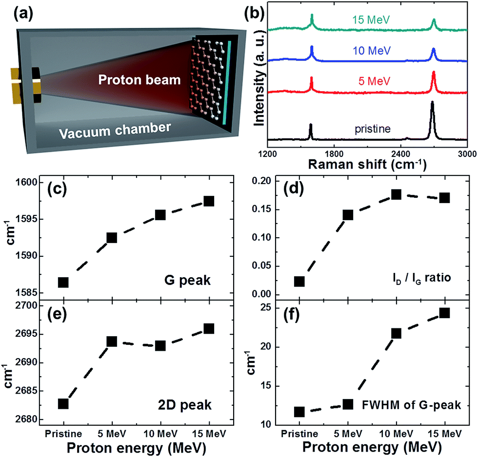 | ||
| Fig. 1 (a) Schematic diagram of proton irradiation of monolayer graphene/SiO2/Si substrate inside the vacuum chamber, (b) Raman spectra of graphene before and after 5–15 MeV proton irradiation with a dose of 1 × 1016 cm−2, (c) position of G peak, (d) intensity ratio of D to G peak (ID/IG), (e) position of 2D peak, and (f) FWHM of G peak plotted for pristine and proton-irradiated graphene at different proton irradiation energies. | ||
We performed plane-wave density functional theory (DFT) calculations using the Vienna ab initio Simulation Package (VASP).21,22 Exchange-correlation energies were treated by Perdew–Burke–Ernzerhof (PBE) function based on generalized gradient approximation (GGA).23 A plane wave expansion with a cutoff of 400 eV was used with a 2 × 2 × 1 Monkhorst–Pack24 k-point sampling of the Brillouin zone, which was sufficient to give well converged results. Total energy calculations used the residual minimization method for electronic relaxation and geometries were relaxed using a conjugate gradient algorithm until the forces on all unconstrained atoms were less than 0.03 eV Å−1. In order to take into account for dispersion force, we used semi-empirical DFT-D2 method proposed by Grimme.25 We used a graphene unit cell of 72 carbon atoms. The x–y size of the supercell was 14.80 Å × 12.82 Å. The vacuum thickness of 17 Å was used to decouple the periodic images of the slab surfaces. The defect formation energy of graphene (Ef) was calculated from the total energies of the supercells with a defect,26
| Ef = Ed − Ep − nμ | (1) |
3. Results and discussion
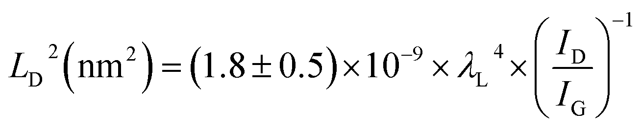
Fig. 1(b) shows the evolution of Raman spectra of the graphene before and after proton irradiation with energies of 5, 10, and 15 MeV at a fixed dose of 1 × 1016 cm−2. The Raman spectra of pristine graphene generally had two main peaks: the G peak (∼1585 cm−1) and the 2D peak (∼2680 cm−1). The thickness of the pristine graphene was estimated using the typical features of monolayer graphene: (i) a 2D-to-G-peak intensity ratio of ∼2.3 and (ii) a symmetric 2D band centered at 2683 cm−1 with a full-width-at-half-maximum (FWHM) of ∼28 cm−1.27 In addition, the D peak at ∼1356 cm−1, which reflects the existence of the Raman active defects, was ignorable in the case of pristine graphene, as shown in Fig. 1(b). In Fig. 1(d), the intensity ratio (ID/IG) of the D peak to the G peak, which serves as the conventional criterion for analyzing defects or disorder in graphene,11,28 increases from 0.02 to 0.17 with increasing proton energy. In addition, the changes in the FWHM of the G peak indicate structural disordering of the graphene with increasing proton energy,28,29 although the FWHM of the G peak can vary with the doping of graphene.30 As shown in Fig. 1(f), the FWHM of the G peak increased from 12 cm−1 to 24 cm−1, which can be explained by the increase in the defect density after 15 MeV proton irradiation. Therefore, the disorder in the graphene increased with increasing proton irradiation energy up to 15 MeV in our experiment. Fig. 1(c) and (e) show that proton irradiation shifted the G and 2D peaks upward, which implies unintentional chemical doping of the graphene when the irradiated samples were stored in an air ambient. The doping polarity can be determined by correlating the peak positions of the G and 2D bands, where the upshifts of both the G and 2D peaks indicate p-doping by charge transfer between the adsorbed molecules and the graphene.31,32Disorder induced by proton irradiation is schematically illustrated in Fig. 2(a). The amorphization trajectory of carbon materials when defects were introduced was previously reported using Raman spectroscopy.28,33,34 Fig. 2(b) shows the evolution of Raman spectra of graphene before and after 10 MeV proton irradiation with various doses from 1 × 10¹⁶ to 3 × 1016 cm−2. The characteristics of high-quality monolayer graphene were confirmed by three features: (i) the 2D-to-G-peak intensity ratio is ∼1, (ii) the symmetric 2D band is centered at 2681 cm−1 with an FWHM of ∼35 cm−1, and (iii) the D peak at 1350 cm−1 is ignorable. Fig. 2(d) and (f) show that ID/IG is consistent with the FWHM of the G peak at increasing doses, indicating more damage at higher doses. In Fig. 2(c) and (e), the positions of the G and 2D peaks imply p-doping of the irradiated graphene for the reasons mentioned above. Fig. 2(d) shows that ID/IG increases with increasing proton irradiation dose owing to the increase in the defect density. Under a low-defect-density regime [LD (average defect distance) ≥ 10 nm], since the ratio of ID/IG is inversely proportional to LD2, LD can be estimated by using the equation,34
 | (2) |
 | ||
| Fig. 2 (a) Schematic diagram of defective graphene under proton irradiation, (b) Raman spectra of graphene before and after 10 MeV proton irradiation with doses of 1 × 10¹⁶ to 3 × 1016 cm−2, (c) position of G peak, (d) intensity ratio of D to G peak (ID/IG), (e) position of 2D peak, and (f) FWHM of G peak plotted for pristine and proton-irradiated graphene at varying doses. | ||
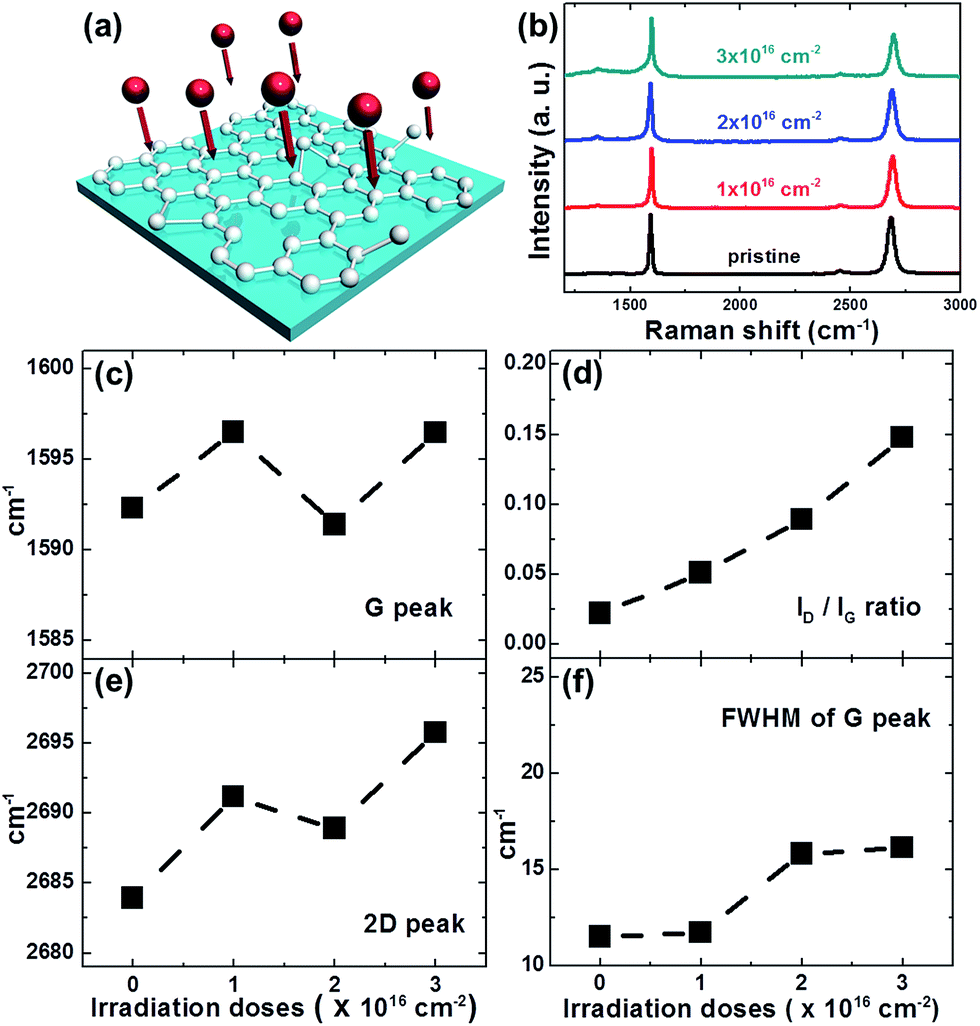
In order to identify the type of defects induced by proton irradiation, we performed DFT calculations. The formation of various types of defects was compared by calculating the defect formation energies as described in eqn (1). With this definition, lower defect formation energy implies easier formation of the defect. We considered three types of defect models as reported in previous literatures (Fig. 3(b)); reconstructed, vacancy, and adatom–vacancy pair models. The formation energy of each defect is summarized in Fig. 3(a). First, reconstructions are occurred by rotating or breaking and recombination of C–C bonds. The possible models are Stone–Wales (SW) (Ef = 5.11 eV) and 7-5-4-8 (Ef = 10.96 eV) and 5-7-7-4-4-9 (Ef = 12.61 eV) models.12,35–38 The 7-5-4-8 and 5-7-7-4-4-9 models contain two different shapes of rectangle and octagon, instead of normal hexagon. Meanwhile, the SW defect is formed by 90° rotation of only one C–C bond. This exhibits the smallest defect formation energy, implying the most probable defect to be formed among the various defects we examine. Second, vacancy models involve the formation of carbon vacancy. The single vacancy (SV or 5-9) misses one lattice carbon atom (Ef = 7.94 eV) while the double vacancy (5-8-5) loses the adjacent two lattice carbon atoms (Ef = 7.94 eV).12,35,39,40 Both models break C–C bonds to form the dangling bonds involved in a void area. The 555-777 (Ef = 6.80 eV) is also related to the missing of two lattice carbon atoms, but followed by the formation of vacancies, the rearrangement of carbon atoms near the vacancies is additionally occurred without breaking the C–C bonds. Last, adatom–vacancy pair models include both vacancy and adatom (interstitial) atoms, which has been experimentally observed before.41 The M1 (SV or 5-9) model (Ef = 13.99 eV) has a pair form of one SV vacancy and one carbon adatom on the interstitial site while the M1 (5-8-5) (Ef = 16.52 eV) and M2 (5-8-5) (Ef = 16.38 eV) models are involved in two 5-8-5 vacancies and two adatoms on the adjacent interstitial sites. Since these models involve two processes of creating vacancies and then moving them to the nearby interstitial sites as adatoms, high defect formation energies (>13 eV) are required, compared to the other defect models. In the view of thermodynamics, the energy required to form one more carbon vacancy from SV to 5-8-5 in the vacancy models is almost zero. However, the adatom–vacancy pair model (M1 or M2) can be approximately considered as a transition states of the process, which is energetically higher than SV by ∼8.5 eV. Thus, the process from SV to 5-8-5 is not a barrier-free process. Based on our DFT results, the defects formed by reconstructing the C–C bonds such as SW would occupy the large portion of defects created on the monolayer graphene after proton irradiation. However, the types of the defects might have less dependence on Ef because the proton irradiation energy is much higher than Ef. Incident angle and irradiation energies also need to be considered.42,43
 | ||
| Fig. 3 (a) Defect formation energies of various defect models. (b) The reconstructed models are Stone–Wales, 7-5-4-8 and 5-7-7-4-4-9 (topological defects). The vacancy models are 5-9 (single vacancy), 5-8-5, and 555-777 (double vacancies). The adatom–vacancy pair models are M1 (SV or 5-9), M1 (5-8-5), and M2 (5-8-5). Normal C atoms are shown as gray spheres, defect region as yellow spheres, and adatoms as blue spheres, respectively. | ||
The changes in the chemical bonding states of the graphene by proton irradiation were analyzed by XPS. Fig. 4(a) and (b) show the C1s core-level XPS spectra of the graphene layer before and after 10 MeV proton irradiation with a dose of 3 × 1016 cm−2, respectively. The C1s core peaks were divided into five symmetric Gaussian curves: a predominant sp2 C–C (binding energy EB = 284.4 eV), C–O (EB = 285.3 eV), C–O (EB = 286.4 eV), C![[double bond, length as m-dash]](https://www.rsc.org/images/entities/char_e001.gif) O (EB = 288.2 eV), and HO–CO (EB = 289.2 eV).44,45 As shown in Fig. 4(a) and (b), the peak area ratio of sp2 C–C bonding decreased from 63.3% to 57.9% because of the proton-irradiation-induced defects, which is in good agreement with the results for graphene subjected to helium ion bombardment.46 The peak area ratios of C–O (EB = 285.3 eV) and CO for the proton-irradiated graphene increased from 19.4% and 1.9% to 25.6% and 3.6%, respectively. The p-type doping effects can be attributed to the charge transfer between the C bonds and the environmental molecules including oxygen and vapor.47 Especially, the interaction between the graphene and the environmental molecules can be enhanced by the defect-induced modification of the C bonds in graphene.48 Therefore, we believe that passivation of the graphene using inert materials can minimize the charge transfer when it is exposed to high-energy proton irradiation.
O (EB = 288.2 eV), and HO–CO (EB = 289.2 eV).44,45 As shown in Fig. 4(a) and (b), the peak area ratio of sp2 C–C bonding decreased from 63.3% to 57.9% because of the proton-irradiation-induced defects, which is in good agreement with the results for graphene subjected to helium ion bombardment.46 The peak area ratios of C–O (EB = 285.3 eV) and CO for the proton-irradiated graphene increased from 19.4% and 1.9% to 25.6% and 3.6%, respectively. The p-type doping effects can be attributed to the charge transfer between the C bonds and the environmental molecules including oxygen and vapor.47 Especially, the interaction between the graphene and the environmental molecules can be enhanced by the defect-induced modification of the C bonds in graphene.48 Therefore, we believe that passivation of the graphene using inert materials can minimize the charge transfer when it is exposed to high-energy proton irradiation.
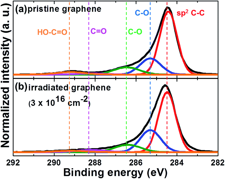 | ||
| Fig. 4 XPS data of C1s core level for (a) pristine and (b) 10 MeV proton-irradiated graphene at a dose of 3 × 1016 cm−2. | ||
4. Conclusion
The dependence of radiation-induced damage in monolayer graphene on both the proton energy and dose was systematically investigated by applying various energies and doses and using micro-Raman spectroscopy and XPS. The increase in ID/IG and wider FWHM of the G peak indicated that the disorder in the graphene increased with increasing the proton dose and energy. Defect formation energies of various defect models were compared by DFT calculation. Also, we observed that electron-withdrawing molecules were adsorbed on proton-irradiated graphene, making the damaged graphene p-type after proton irradiation.Acknowledgements
This research was supported by grants from the Basic Science Research Program (2012R1A1A2042761), the Radiation Technology Research and Development program (2013M2A2A6043608) through the National Research Foundation of Korea funded by the Ministry of Science, Information Communication Technology & Future Planning for Jihyun Kim and the 2013 Research Fund of the University of Seoul for Jeong Woo Han.References
- C. Clayes and E. Simoen, Radiation effects in advanced semiconductor materials and devices, Springer, 2002 Search PubMed.
- S. J. Pearton, R. Deist, F. Ren, L. Liu, A. Y. Polyakov and J. Kim, J. Vac. Sci. Technol., A, 2013, 31, 050801 Search PubMed.
- A. Y. Polyakov, S. J. Pearton, P. Frenzer, F. Ren, L. Liu and J. Kim, J. Mater. Chem. C, 2013, 1, 877–887 RSC.
- F. Schwierz, Nat. Nanotechnol., 2010, 5, 487–496 CrossRef CAS PubMed.
- F. Bonaccorso, Z. Sun, T. Hasan and A. C. Ferrari, Nat. Photonics, 2010, 4, 611–622 CrossRef CAS.
- A. H. Reshak, S. A. Khan and S. Auluck, J. Mater. Chem. C, 2014, 2, 2346–2352 RSC.
- K. S. Novoselov, V. I. Fal'ko, L. Colombo, P. R. Gellert, M. G. Schwab and K. Kim, Nature, 2012, 490, 192–200 CrossRef CAS PubMed.
- A. H. Reshak and S. Auluck, Mater. Express, 2014, 4, 508–520 CrossRef CAS PubMed.
- A. H. Reshak and S. Auluck, J. Appl. Phys., 2014, 116, 103702 CrossRef PubMed.
- A. H. Reshak, S. A. Khan and S. Auluck, RSC Adv., 2014, 4, 11967–11974 RSC.
- A. Eckmann, A. Felten, A. Mishchenko, L. Britnell, R. Krupke, K. S. Novoselov and C. Casiraghi, Nano Lett., 2012, 12, 3925–3930 CrossRef CAS PubMed.
- F. Banhart, J. Kotakoski and A. V. Krasheninnikov, ACS Nano, 2011, 5, 26–41 CrossRef CAS PubMed.
- S. Wang, B. Yang, S. Zhang, J. Yuan, Y. Si and H. Chen, ChemPhysChem, 2014, 15, 2749–2755 CrossRef CAS PubMed.
- B. Yang, S. Wang, Y. Guo, J. Yuan, Y. Si, S. Zhang and H. Chen, RSC Adv., 2014, 4, 54677–54683 RSC.
- V. A. Basiuk, K. Kobayashi, T. Kaneko, Y. Negishi, E. V. Basiuk and J.-M. Saniger-Blesa, Nano Lett., 2002, 2, 789–791 CrossRef CAS.
- B. Khare, M. Meyyappan, M. H. Moore, P. Wilhite, H. Imanaka and B. Chen, Nano Lett., 2003, 3, 643–646 CrossRef CAS.
- W.-K. Hong, C. Lee, D. Nepal, K. E. Geckeler, K. Shin and T. Lee, Nanotechnology, 2006, 17, 5675–5680 CrossRef CAS PubMed.
- S. Mathew, T. K. Chan, D. Zhan, K. Gopinadhan, A. R. Barman, M. B. H. Breese, S. Dhar, Z. X. Shen, T. Venkatesan and J. T. L. Thong, J. Appl. Phys., 2011, 110, 084309 CrossRef PubMed.
- S. Mathew, T. K. Chan, D. Zhan, K. Gopinadhan, A.-R. Barman, M. B. H. Breese, S. Dhar, Z. X. Shen, T. Venkatesan and J. T. L. Thong, Carbon, 2011, 49, 1720–1726 CrossRef CAS PubMed.
- G. Ko, H.-Y. Kim, F. Ren, S. J. Pearton and J. Kim, Electrochem. Solid-State Lett., 2010, 13, K32–K34 CrossRef CAS PubMed.
- G. Kresse and J. Furthmüller, Phys. Rev. B: Condens. Matter Mater. Phys., 1996, 54, 11169–11186 CrossRef CAS.
- D. S. Sholl and J. A. Steckel, Density functional theory: a practical introduction, John Wiley & Sons, 2009 Search PubMed.
- J. P. Perdew, K. Burke and M. Ernzerhof, Phys. Rev. Lett., 1996, 77, 3865–3868 CrossRef CAS.
- H. J. Monkhorst and J. D. Pack, Phys. Rev. B: Solid State, 1976, 13, 5188–5192 CrossRef.
- S. Grimme, J. Comput. Chem., 2006, 27, 1787–1799 CrossRef CAS PubMed.
- C. G. Van de Walle and J. Neugebauer, J. Appl. Phys., 2004, 95, 3851–3879 CrossRef CAS PubMed.
- Y. Hao, Y. Wang, L. Wang, Z. Ni, Z. Wang, R. Wang, C. K. Koo, Z. Shen and J. T. L. Thong, Small, 2010, 6, 195–200 CrossRef CAS PubMed.
- A. C. Ferrari and D. M. Basko, Nat. Nanotechnol., 2013, 8, 235–246 CrossRef CAS PubMed.
- A. C. Ferrari, S. E. Rodil and J. Robertson, Phys. Rev. B: Condens. Matter Mater. Phys., 2003, 67, 155306 CrossRef.
- H. Liu, Y. Liu and D. Zhu, J. Mater. Chem., 2011, 21, 3335–3345 RSC.
- A. Das, S. Pisana, B. Chakraborty, S. Piscanec, S. K. Saha, U. V. Waghmare, K. S. Novoselov, H. R. Krishnamurthy, A. K. Geim, A. C. Ferrari and A. K. Sood, Nat. Nanotechnol., 2008, 3, 210–215 CrossRef CAS PubMed.
- B.-J. Kim, G. Yang, H.-Y. Kim, K. H. Baik, M. A. Mastro, J. K. Hite, C. R. Eddy Jr, F. Ren, S. J. Pearton and J. Kim, Opt. Express, 2013, 21, 29025–29030 CrossRef PubMed.
- A. C. Ferrari and J. Robertson, Phys. Rev. B: Condens. Matter Mater. Phys., 2001, 64, 075414 CrossRef.
- L. G. Cançado, A. Jorio, E. H. M. Ferreira, F. Stavale, C. A. Achete, R. B. Capaz, M. V. O. Moutinho, A. Lombardo, T. S. Kulmala and A. C. Ferrari, Nano Lett., 2011, 11, 3190–3196 CrossRef PubMed.
- J. C. Meyer, C. Kisielowski, R. Erni, M. D. Rossell, M. F. Crommie and A. Zettl, Nano Lett., 2008, 8, 3582–3586 CrossRef CAS PubMed.
- L. Li, S. Reich and J. Robertson, Phys. Rev. B: Condens. Matter Mater. Phys., 2005, 72, 184109 CrossRef.
- O. V. Yazyev, I. Tavernelli, U. Rothlisberger and L. Helm, Phys. Rev. B: Condens. Matter Mater. Phys., 2007, 75, 115418 CrossRef.
- J. Ma, D. Alfè, A. Michaelides and E. Wang, Phys. Rev. B: Condens. Matter Mater. Phys., 2009, 80, 033407 CrossRef.
- M. M. Ugeda, I. Brihuega, F. Guinea and J. M. Gómez-Rodríguez, Phys. Rev. Lett., 2010, 104, 096804 CrossRef CAS.
- J. Kotakoski, A. V. Krasheninnikov, U. Kaiser and J. C. Meyer, Phys. Rev. Lett., 2011, 106, 105505 CrossRef CAS.
- A. Hashimoto, K. Suenaga, A. Gloter, K. Urita and S. Iijima, Nature, 2004, 430, 870–873 CrossRef CAS PubMed.
- Y. Asayama, M. Yasuda, K. Tada, H. Kawata and Y. Hirai, J. Vac. Sci. Technol., B: Nanotechnol. Microelectron.: Mater., Process., Meas., Phenom., 2012, 30, 06FJ02 Search PubMed.
- M. Yamamoto, Y. Asayama, M. Yasuda, H. Kawata and Y. Hirai, J. Vac. Sci. Technol., B: Nanotechnol. Microelectron.: Mater., Process., Meas., Phenom., 2014, 32, 06FK01 Search PubMed.
- D. Yang, A. Velamakanni, G. Bozoklu, S. Park, M. Stoller, R. D. Piner, S. Stankovich, I. Jung, D. A. Field, C. A. Ventrice Jr and R. S. Ruoff, Carbon, 2009, 47, 145–152 CrossRef CAS PubMed.
- T. Zhou, F. Chen, K. Liu, H. Deng, Q. Zhang, J. Feng and Q. Fu, Nanotechnology, 2011, 22, 045704 CrossRef PubMed.
- J.-H. Kim, J. H. Hwang, J. Suh, S. Tongay, S. Kwon, C. C. Hwang, J. Wu and J. Y. Park, Appl. Phys. Lett., 2013, 103, 171604 CrossRef PubMed.
- H. Chen and E. Ruckenstein, J. Phys. Chem. Lett., 2014, 5, 2979–2982 CrossRef CAS.
- Y.-H. Zhang, Y.-B. Chen, K.-G. Zhou, C.-H. Liu, J. Zeng, H.-L. Zhang and Y. Peng, Nanotechnology, 2009, 20, 185504 CrossRef PubMed.
| This journal is © The Royal Society of Chemistry 2015 |