Highly flexible and conductive composite films of silk fibroin and silver nanowires for optoelectronic devices

Ning Qia, Bing Zhaoa, Shu-Dong Wangab, Salem S. Al-Deyabc and Ke-Qin Zhang*ad
aNational Engineering Laboratory for Modern Silk, College of Textile and Clothing Engineering, Soochow University, Suzhou 215123, China. E-mail: kqzhang@suda.edu.cn
bCollege of Textile and Clothing, Yancheng Institute of Industry Technology, Yancheng 224005, China
cDepartment of Chemistry, College of Science, King Saud University, Riyadh 11451, Saudi Arabia
dResearch Center of the Cooperative Innovation for Functional Organic/Polymer Material Micro/Nanofabrication, Soochow University, Suzhou, Jiangsu 215123, China

Received 26th February 2015 , Accepted 3rd June 2015

First published on 3rd June 2015


Abstract

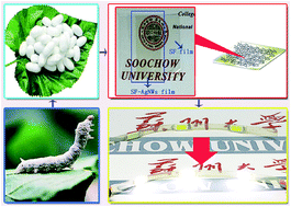
Silver nanowire-coated silk fibroin (SF) was used to create composite films with high flexibility, good electrical conductivity and excellent mechanical properties. SF was coated with a layer of entangled silver nanowires (AgNWs) that were sputtered with a platinum layer. The SF–AgNWs composite films exhibited excellent performance with a conductivity of ∼15.0 Ω sq−1 and transmittance of ∼80% in the visible light range. The films also retained conductivity even after being bent hundreds of times; this recovery was attributed to the structure of the embedded AgNWs in SF, and metallic contacts among the AgNWs induced by the ion sputtering. The SF–AgNWs composite films also showed promise in practical applications, including as a conduit to light emitting diodes (LEDs). These novel composite films could be used to fabricate wearable electronics and implantable devices.


Introduction

Substrates play a key role in the fabrication of optoelectronic devices. Glass, plastic (PET, PVP, PVA, PEN), paper, and textiles are usually chosen as substrates.1–6 Plastic is a commercially popular substrate made from non-renewable resources, but its limitations have become increasingly problematic. Further research is required to find a viable alternative to plastic. Silk fibroin (SF) is a natural macromolecular fibrous protein derived from silkworm (Bombyx mori) cocoons. SF displays excellent mechanical and optical properties, as well as biocompatibility, biodegradability and implantability;7 it can be processed into various forms such as gels, strands, sponges, blocks, foams and films. Natural SF can be more easily acquired and controlled than plastic. SF can be formed into flexible and transparent films (with over 90% transmission in visible light range); the processes to form such films are simple and unique.8 The strength of SF is far superior to the other substrate materials, and its special structural characteristics and outstanding physical properties make SF advantageous in optoelectronics applications.

SF-based transparent conducting electrodes have not yet been heavily explored in research, and there is a lack of literature on this topic. Jia et al.9 previously reported producing flexible transparent conducting thin films composed of reduced graphene oxide (RGO) and SF. The measured surface resistance of these composite films is approximately 1000 Ω sq−1, which is much higher than the surface resistance of commercial indium tin oxide (ITO)–glass substrates.

Highly flexible transparent electrodes are especially desirable for use in flexible optoelectronic devices. Although ITO-based optoelectronic devices are common due to ITO's high optical transparency and low sheet resistance, the brittleness of ITO films and scarcity of indium resources limit the sustainability of its use. Therefore, some researchers have focused on developing candidates to replace ITO, including carbon nanotubes (CNTs),10 graphene,11–14 and metal nanowires.15–17 Silver nanowires (AgNWs) are particularly advantageous due to its ability to produce a nanotrough network. This nanotrough network can form a foldable, conductive, reliable and transparent conducting electrode layer that can adsorb on or be buried into the surfaces of various substrate materials.18,19

In this research, SF films were used as substrates in place of glass, synthetic polymers and flexible bases. AgNWs were sputtered with platinum to form the better conductive network, then subsequently embedded into SF to build composite films. The interfacial structure, tensile mechanical property and thermogravimetric property of such composite films were characterized and compared with various existing substrates. Most importantly, the composite films exhibited the desired conductivity and excellent transparency in the visible light range; the conductivity and transparency was comparable to commercial ITO substrates. The composite films retained conductivity after being bent and unbent 100 times, presenting much better flexibility than other polymeric substrates. To demonstrate future possibilities in flexible electrodes, conducting materials, and implantable devices, LED chips were fabricated on the AgNWs and SF thin film.20,22

Results and discussion

Each step in the preparation of SF–AgNWs composite films is shown in Fig. 1. The AgNWs were spin-coated onto the surface of a silicon plate (Fig. 1(a)), and the plate was sputtered with Pt film (Fig. 1(b)), then immersed in SF solution (Fig. 1(c)). SF–AgNWs composite films formed after water evaporation (Fig. 1(d)), and were stripped from the silicon plate (Fig. 1(e)). This process insured that the AgNWs nanotrough network had good adhesion and bonding with the SF films.
image file: c5ra03501e-f1.tif
Fig. 1 (a) AgNWs solution was spin-coated onto the silicon wafer, (b) the plate was sputtered with Pt film, (c) SF aqueous solution dropped onto the AgNWs-coated wafer substrate, (d) SF–AgNWs composite film formed after water evaporation, (e) the SF–AgNWs film was obtained after stripping from the substrate, (f) high-resolution TEM of AgNWs and (g), SEM micrographs of AgNWs embedded in SF film, (h) SEM micrographs of SF film thicknesses.

Morphology and characterization

AgNW diameters ranged from 30 to 40 nm (Fig. 1(f and g)), and lengths varied from 1 to 2 μm. SEM images show that AgNWs were well buried in the SF films (Fig. 1(g)). After being buried at the surface of SF, the intrinsically fragile network of AgNWs became mechanically robust because they were firmly anchored by the SF matrix.21 The thicknesses of the SF films were approximately 10–20 μm (Fig. 1(h)); due to their nanostructured configuration, AgNWs have insignificant effect on film thickness.

Mechanical properties

The tensile mechanical properties of SF and SF–AgNWs films are shown in Fig. 2. The breaking stress of the films was measured to be more than 70 MPa, with an elongation at break of around 3%. The breaking elongation curve of the SF–AgNWs films is similar to SF films, indicating that the mechanical properties that mainly depended on SF and AgNWs had insignificant effect on the mechanical performance of the composite films. Due to the difference in fracture modes, the mechanical properties of SF–AgNWs films are superior to PET films.
image file: c5ra03501e-f2.tif
Fig. 2 The stress–strain curve of SF film, SF–AgNWs film and PET substrate.

Thermogravimetric properties

The thermogravimetric curves of studied materials are presented in Fig. 3, the measurements were obtained from room temperature to 600 °C at a heating rate of 10 °C min−1 in a nitrogen atmosphere. AgNWs films display similar thermal stability as SF due to being comprised of the same material. From the room temperature to 100 °C, the curve displayed about 10% of weight loss because of water evaporation from the SF films. However, the PET film did not lose mass due to low moisture content. As temperature was increased, both SF and SF–AgNWs films showed sharp decline in weight loss at around 270 °C, due to the thermal degradation of silk proteins.22 The PET film's different thermal stability started rapid decomposition at about 420 °C.
image file: c5ra03501e-f3.tif
Fig. 3 The Tg curves of SF film, SF–AgNWs film and PET film.

Transmittance of the SF–AgNWs

As shown in Fig. 4, pure SF films displayed excellent visible light transmittance of 90%. This value is comparable to the transmittance of glass, PET, synthetic polymers and other clear substrates, making SF film a viable replacement for these common transparent substrates. The SF–AgNWs films displayed a transmittance of 80% in the visible light range, which is weaker than the transmittance of pure SF films. This effect is due to shielding from the AgNWs network, which absorb and reflect light. There is an obvious absorption peak at 375 nm due to the natural plasmonic effects of the AgNWs networks caused by light trapping.23 However, the transparency of the SF–AgNWs films is similar to that of ITO–glass in the visible spectrum.
image file: c5ra03501e-f4.tif
Fig. 4 The optical transmittance spectra of SF films, SF–AgNWs films and ITO–glass.

Conductivity and flexibility

Fig. 5(a) shows that the resistance of the SF–AgNWs films (∼15.0 Ω sq−1) is comparable to ITO–glass (∼11.0 Ω sq−1) and ITO–PEN (∼15.0 Ω sq−1), and better than magnetron sputtering-deposited Au (∼32.0 Ω sq−1) and Pt (∼155.0 Ω sq−1) films (at 10 mA, 180 s) on SF substrates. After a bending test consisting of bending and unbending 100 times, the conductivity of the SF–AgNWs films stayed consistent at 18.0 Ω sq−1 without obvious increase; this is better than the performance of previous reported results. However, the resistance of other films increased to 500.0 Ω sq−1 and more after being subject to the same bending test. The excellent conductivity retention of AgNW–SF following mechanical stress is attributed to the embedded AgNWs in the protein substrate,24 ductility of silver, and excellent contact among the AgNWs as a result of platinum sputtering.
image file: c5ra03501e-f5.tif
Fig. 5 (a) Comparison of resistance of different conductive substrates before and after bending, operated by the KES-F hand meter as shown in the first row. (b) Lighting the LEDs by applying the electric current on the SF–AgNWs composite film.

Commercial LED chips were embedded on the SF–AgNWs films strips to form a conductive network circuit; the film was able to successfully light the LED chips (Fig. 5(b)). This indicates its ability to provide power to other optoelectronic devices. This luminescent strip can be bent or folded, catering to various wearable applications.

Experimental

Fabrication of composite thin film

Ag nanowires (0.5 mg ml−1) solution was spin-coated (3000–3500 rpm) onto a polished silicon wafer substrate, then sputtered with platinum (10 mA, 10–20 s). After the platinum was adsorbed onto the substrate, the wafer attained a nanotrough network layer of AgNWs. The SF aqueous solution was prepared as previously described (silkworm cocoon can be used to synthesize SF solution by dissolution and dialysis after silk degumming),25 then dropped onto the AgNWs-coated wafer substrate. The substrate was carefully removed after the solution dried.

Fabrication of LED strip

A regular conductive strip with a width of 5 mm was cut from rectangular SF–AgNWs film using scissors. The strip was used to connect the commercial LED chips by embedding the electrodes on the conductive substrates. Then a direct current of 5.0 V was applied into the two ends of the strip.

Measurement and analysis instruments

The morphology of the SF–AgNWs composite films was examined using a field emission scanning electron microscope (S-4800, Hitachi, Japan) and a transmission electron microscope (HT7700, Hitachi, Japan). The mechanical properties were measured using universal testing systems (5967, Instron, America), the test samples were made into 10 mm × 40 mm from the rectangular films. The transmittance spectrum was measured by a UV-VIS spectrophotometer (UV2550, Shimadzu, Japan). The thermogravity properties were analyzed by a thermal gravimetric analyzer (Q600, TA, America). The resistance was tested by four-point probe method. Bending test for evaluating the film's flexibility was measured using a KES-F hand meter (KES-FB4, KATO, Japan).

Conclusions

In summary, this research demonstrates a spin-coating method combining metallic deposition, to prepare SF–AgNWs composite films. Compared to existing hard and flexible substrates, these composite films displayed excellent transmittance and conductivity retention even after tremendous stress. The films could be used as a basis in further development of wearable textile and conducting devices. With continued research and focus in this area, it is possible to create flexible electronics and wearable textiles based on the high performance, biocompatible SF–AgNWs composite films.23

Acknowledgements

This research was financially supported by the National Natural Science Foundation of China under grant 51073113, 91027039 and 51373110, the Natural Science Foundation of the Jiangsu Higher Education Institutions of China (10KJA540046) and the Nanotechnology Foundation of Suzhou under Grant ZXG2013037. The authors extend their appreciation to the Deanship of Scientific Research at King Saud University for funding this work through the research group project no. RGP-089. We also acknowledge the fund from the project of the Priority Academic Program Development of Jiangsu Higher Education Institutions (PAPD), Qing Lan Project for Excellent Scientific and Technological Innovation Team of Jiangsu Province (2012) and Project for Jiangsu Scientific and Technological Innovation Team (2013).

Notes and references

  1. H. Wu, D. Kong, Z. Ruan, P. Hsu, S. Wang, Z. Yu, T. J. Carney, L. Hu, S. Fan and Y. Cui, Nat. Nanotechnol., 2013, 8, 421–425 CrossRef CAS PubMed.
  2. Z. Fang, H. Zhu, Y. Yuan, D. Ha, S. Zhu, C. Preston, Q. Chen, Y. Li, X. Han, S. Lee, G. Chen, T. Li, J. Munday, J. Huang and L. Hu, Nano Lett., 2014, 14, 765–773 CrossRef CAS PubMed.
  3. Y. Jin, D. Deng, Y. Cheng, L. Kong and F. Xiao, Nanoscale, 2014, 6, 4812–4818 RSC.
  4. M. C. Barr, J. A. Rowehl, R. R. Lunt, J. Xu, A. Wang, C. M. Boyce, S. G. Im, V. Bulović and K. K. Gleason, Adv. Mater., 2011, 23, 3500–3505 CrossRef CAS PubMed.
  5. A. Hübler, B. Trnovec, T. Zillger, M. Ali, N. Wetzold, M. Mingebach, A. Wagenpfahl, C. Deibel and V. Dyakonov, Adv. Energy Mater., 2011, 1, 1018–1022 CrossRef PubMed.
  6. Y. Zhou, C. Fuentes-Hernandez, T. M. Khan, J. Liu, J. Hsu, J. W. Shim, A. Dindar, J. P. Youngblood, R. J. Moon and B. Kippelen, Sci. Rep., 2013, 3, 1536–1541 Search PubMed.
  7. F. G. Omenetto and D. L. Kaplan, Nat. Photonics, 2008, 2, 641–643 CrossRef CAS PubMed.
  8. B. D. Lawrence, M. Cronin-Golomb, I. Georgakoudi, D. L. Kaplan and F. G. Omenetto, Biomacromolecules, 2008, 9, 1214–1220 CrossRef CAS PubMed.
  9. M. Jia, N. Qi, Q. Dong, H. Wang and K. Zhang, Int. J. Nanotechnol., 2014, 11, 298–310 CrossRef CAS.
  10. Y. C. Jung, D. Shimamoto, H. Muramatsu, Y. A. Kim, T. Hayashi, M. Terrones and M. Endo, Adv. Mater., 2008, 20, 4509–4512 CrossRef CAS PubMed.
  11. L. Gomez De Arco, Y. Zhang, C. W. Schlenker, K. Ryu, M. E. Thompson and C. Zhou, ACS Nano, 2010, 4, 2865–2873 CrossRef CAS PubMed.
  12. Y. Liang, J. Frisch, L. Zhi, H. Norouzi-Arasi, X. Feng, J. P. Rabe, N. Koch and K. Müllen, Nanotechnology, 2009, 20, 434007–434012 CrossRef PubMed.
  13. X. Wang, L. Zhi and K. Müllen, Nano Lett., 2008, 8, 323–327 CrossRef CAS PubMed.
  14. X. Wang, L. Zhi, N. Tsao, Ž. Tomović, J. Li and K. Müllen, Angew. Chem., Int. Ed., 2008, 47, 2990–2992 CrossRef CAS PubMed.
  15. H. Wu, L. Hu, M. W. Rowell, D. Kong, J. J. Cha, J. R. McDonough, J. Zhu, Y. Yang, M. D. McGehee and Y. Cui, Nano Lett., 2010, 10, 4242–4248 CrossRef CAS PubMed.
  16. D. S. Hecht, L. Hu and G. Irvin, Adv. Mater., 2011, 23, 1482–1513 CrossRef CAS PubMed.
  17. K. Ellmer, Nat. Photonics, 2012, 6, 809–817 CrossRef CAS PubMed.
  18. W. Gaynor, G. F. Burkhard, M. D. McGehee and P. Peumans, Adv. Mater., 2011, 23, 2905–2910 CrossRef CAS PubMed.
  19. S. De, T. M. Higgins, P. E. Lyons, E. M. Doherty, P. N. Nirmalraj, W. J. Blau, J. J. Boland and J. N. Coleman, ACS Nano, 2009, 3, 1767–1774 CrossRef CAS PubMed.
  20. C. Jiang, X. Wang, R. Gunawidjaja, Y. H. Lin, M. K. Gupta, D. L. Kaplan, R. R. Naik and V. V. Tsukruk, Adv. Funct. Mater., 2007, 17, 2229–2237 CrossRef CAS PubMed.
  21. X. Zeng, Q. Zhang, R. Yu and C. Lu, Adv. Mater., 2010, 22, 4484–4488 CrossRef CAS PubMed.
  22. L. Li, K. Wei, F. Lin, X. Kong and J. Yao, J. Mater. Sci.: Mater. Med., 2008, 19, 577–582 CrossRef CAS PubMed.
  23. R. Capelli, J. J. Amsden, G. Generali, S. Toffanin, V. Benfenati, M. Muccini, D. L. Kaplan, F. G. Omenetto and R. Zamboni, Org. Electron., 2011, 12, 1146–1151 CrossRef CAS PubMed.
  24. Y. Liu, N. Qi, T. Song, M. Jia, Z. Xia, Z. Yuan, W. Yuan, K. Zhang and B. Sun, ACS Appl. Mater. Interfaces, 2014, 6, 20670–20675 CAS.
  25. S. Yan, Q. Zhang, J. Wang, Y. Liu, S. Lu, M. Li and D. L. Kaplan, Acta Biomater., 2013, 9, 6771–6782 CrossRef CAS PubMed.

This journal is © The Royal Society of Chemistry 2015
Click here to see how this site uses Cookies. View our privacy policy here.