
Scalable synthesis of two-dimensional antimony telluride nanoplates down to a single quintuple layer
Fan Yang a,
Robin B. Jacobs-Gedrima,
Mariyappan Shanmugama,
Nikhil Jaina,
Michael T. Murphya,
Eui Sang Songa,
David Freyb and
Bin Yu*a
a,
Robin B. Jacobs-Gedrima,
Mariyappan Shanmugama,
Nikhil Jaina,
Michael T. Murphya,
Eui Sang Songa,
David Freyb and
Bin Yu*a
aSUNY Polytechnic Institute, USA. E-mail: byu@albany.edu
bRensselaer Polytechnic Institute, USA
First published on 15th June 2015
Abstract
Scalable syntheses of two-dimensional topological insulators are critical to material exploration. We demonstrate a controlled assembly of a two-dimensional V–VI group compound, Sb2Te3 nanoplates (NPs), through a vapor–solid growth process. The physical thickness of Sb2Te3 NPs can be rationally controlled in a wide range, from hundreds of nm down to sub-10 nm. Single-quintuple-layer Sb2Te3 NPs were obtained, with a high domain density of ∼2.465 × 108 cm−2 over a large surface area (1 cm × 1 cm) of a SiO2/Si substrate, verifying a scalable synthesis method. Extensive material analyses were conducted to explore the basic properties of Sb2Te3 NPs using SEM and AFM, etc. HRTEM analysis confirms that the NP samples exhibit a highly crystalline structure and XPS analysis confirms the chemical composition and material stoichiometry. The growth of 2D topological insulator nanostructures may open up new opportunities in surface-state studies and potential applications in low-dissipative electronic systems.
Introduction
As the dimensions of traditional bulk materials decrease, basic physical properties vary due to quantum confinement and surface effects.1 Two-dimensional (2D) atomic crystals are the basic plane structure of bulk layered materials and have attracted significant attention after the discovery of graphene.2–4 A number of 2D nanostructures have been produced, including transitional metal dichalcogenides (TMDCs) (e.g., MoS2)5 and hexagonal boron nitride (h-BN).6,7 Intriguing size-effect dependent properties have been reported in these materials, including non-conventional dielectric behavior,6,7 and tunable energy band-gaps.8 We previously demonstrated extraordinary photoconductive behavior of 2D nanosheets.9 Their unique physical and chemical properties may lead to applications in electronics, photonics, catalytic chemistry, and energy harvesting.10 In2Se3 nanosheets have an extremely high response to visible light, exhibiting a photoresponsivity of 3.95 × 10² A W−1 at 300 nm with an external quantum efficiency greater than 1.63 × 10⁵% at a 5 V bias.Recently, a new family of layer-structured V–VI group compounds has been studied.11,12 Topological insulators (TIs) are a new class of materials in which the surface contains conducting states that behave drastically different from that of the insulating bulk.13–15 While carrier conduction along the surface states is spin-polarized and protected by time-reversal symmetry, TIs potentially enable low-dissipative spintronics and quantum computing.16 Unique phenomena such as the ambipolar field effect, the Aharono–Bohm effect, and the Shubnikov–de Haas oscillation have been observed in ultrathin topological TIs.17–19 Motivated by the potential advantages, we reported the synthesis and electrical characteristics of Bi2Se3 nanoplates (NPs) and nanoribbons.20 Compared to bulk topological insulator materials, ultrathin NPs, especially single quintuple layer (QL) NPs, are highly preferable for studying conduction dominated by surface states due to the very large surface-to-volume ratio.21,22 Controllable syntheses are an essential step toward the exploitation and potential applications of 2D TI nanostructures.
Other than micromechanical exfoliation,15 there are multiple methods for the bottom-up assembly of ultra-thin NPs, including solvo-thermal synthesis,23 chemical vapor deposition,24 atomic layer deposition (ALD)25 and molecular beam epitaxy (MBE).21,26 However, it is difficult for most of these synthesis processes to grow 10 or less QLs of TI materials directly on an insulating substrate (e.g., SiO2) which is desirable for the study of TI properties and device implementation. Great challenges still exist in preparing scalable 2D structures in a controllable manner. To date, the MBE process remains the most effective method to achieve precise layer control.27 Nevertheless, the technique is difficult and expensive. Developing a low-cost process to assemble ultrathin 2D NPs down to a-few-to-single QLs is highly desirable. In this work, we demonstrate a vapor–solid (VS) based method to synthesize 2D antimony telluride (Sb2Te3) NPs directly on a SiO2 surface with controlled thickness. For the first time, the growth of high-density single-QL Sb2Te3 NPs was made possible via the VS process. Moreover, the demonstrated synthesis method could be potentially extended to other 2D TI nanostructures in the binary sesquichalcogenide family.
Experiments
(A) Growth of Sb2Te3 nanoplates
Fig. 1A & B show the schematic of the growth furnace and the thermal processing conditions during the different phases of the process, respectively. Bulk Sb2Te3 pieces (99.999% Alfa Aesar, 36282) were ground into a powder and put in a quartz boat located in the center of the furnace (Lindberg Blue M). The 1 × 1 cm2 SiO2/Si substrate was placed ∼12 cm downstream from the furnace center. The furnace tube was sealed and pumped down to ∼15 mTorr and subsequently flushed with ultra-pure argon several times prior to growth to remove environmental oxygen. We designed a quick ramping up and cooling down growth process to enable a rapidly increasing and decreasing temperature profile. The furnace was moved to the left and heated to over 500 °C in 10 minutes and held at this temperature for another 10 minutes, as shown in Fig. 1A. In the meantime, 50 sccm to 100 sccm argon gas was introduced in the tube. Subsequently, during the growth step the furnace was moved to the right to position the source quartz boat in the furnace center, and evaporation and growth was initiated. The growth time was controlled to within 5 minutes due to the relative fast deposition of Sb2Te3 on the substrate. After the growth step, the furnace was moved away from the source quartz boat and the SiO2/Si substrate to initiate a quick cool down to room temperature in 30 minutes. | ||
| Fig. 1 (A) Schematic diagram of the furnace used for the vapor–solid synthesis of Sb2Te3 NPs. (B) Growth mechanism of the major process sequence for the growth of Sb2Te3 NPs, including the source flow and growth region thermal budget. | ||
(B) Material characterization
The morphology was characterized using a scanning electron microscope (SEM, Hitachi S-4800) and an atomic force microscope (AFM, Veeco Dimension 3100 SPM) in tapping mode. Transmission electron microscopy (TEM, JEOL 2010 Lab6 STEM) and X-ray photoemission spectroscopy (Thermo Scientific Theta Probe Angle-Resolved X-ray Photoelectron Spectrometer System) characterization techniques were used to determine the crystal structure and chemical composition of the as-synthesized NPs. Electronic measurements of the ultrathin NPs were recorded by a Zyvex FIB/SEM sProber.Results and discussion
Previous efforts synthesizing Sb2Te3 nanostructures using a vapor–solid process have yielded hexagonal microplates and NPs with thicknesses of tens of nanometers.28 The size and thickness of as-grown Sb2Te3 domains are mainly controlled by three important parameters: the furnace temperature (T), argon flow rate (JAr), and growth time (t). In order to control the thickness of Sb2Te3 domains, we conducted experiments by using precursor flux and temperature to change the degree of supersaturation of antimony and telluride atoms on the surface of SiO2/Si to yield ultra-thin NPs. After trying several recipes, we obtained isolated NPs rather than a whole film at 550 °C with 100 sccm of argon for 5 minutes of growth time. The synthesized NPs were characterized using SEM and AFM. The SEM image of Fig. 2A shows a high density of as-grown hexagonal Sb2Te3 NPs. The average nanoplate size is ∼4 μm with thickness all greater than 100 nm. The AFM image in the inset shows a height of ∼287 nm. From the AFM data, we see that the surface of the NP is atomically flat, indicating a supersaturating growth process. | ||
| Fig. 2 SEM images (with insets showing AFM images) of Sb2Te3 NPs assembled under different conditions: temperature (°C)/flow rate (sccm)/reaction time (min): (A) 550/100/5, (B) 550/50/5, (C) 550/50/4, and (D) 510/50/4. | ||
To reduce the formation of adlayers, the flow rate was adjusted from 100 sccm to 50 sccm while keeping other parameters the same, as shown in Fig. 2B. The as-grown NPs show an average size of ∼8 μm, larger than during the growth with a decreased flow rate. The AFM measurements confirm that the NP thickness mainly varies from 10 to 40 nm (NP with 10 nm thickness is shown in the Fig. 2B inset). The hexagonal morphology indicates a highly crystalline structure which would be suitable for topological insulator surface studies.29 In addition, the hexagonal shape and flat surface suggest the growth of single crystalline Sb2Te3 NPs (Fig. 2B inset). Under this circumstance, a surface-reaction-limited process is likely to dominate under lower pressure conditions. Besides this, a higher gas velocity induces faster atomic migration on SiO2/Si, resulting in less nucleation sites and more conformal deposition. Therefore, relatively larger size domains with less thickness were obtained.
From the growth results discussed above, the VS growth of Sb2Te3 followed the Volmer–Weber island growth mode. Due to van der Waals bonding between neighboring quintuple layers, the formation energy of adlayer Sb2Te3 is lower on as-grown NPs than on an amorphous SiO2 surface.30 We chose a SiO2/Si substrate in this study. Note that the quantity of vapor source during VS growth determines the NP thickness. To reduce the source supply, the growth duration was reduced to 4 minutes. The SEM image of the synthesized sample is shown in Fig. 2C. Most of the NPs keep the same 120° edge angle with plate size ranging from to 500 nm–3 μm. We noticed that with the reduction in time, an interesting effect occurs. From the AFM line-scan, a ∼5 nm height is detected on the NP edge with ∼10 nm height in the center region. Other than thickness, it appears that these NPs have wrinkled edges. Unlike step-by-step adlayer growth,31 the AFM line-scan data shows smooth elevation from the edge to the center. We assume the existence of a smaller thin plate underneath the large triangular-shaped 5 nm thick NPs. Ripples and wrinkled edges indicate that a smaller domain had nucleated and grown, while the top layers were able to be formed before the growth of the bottom layer was completed.
According to the mechanism of chemical vapor deposition, the deposition rate is inversely proportional to temperature. To further optimize the growth process, we reduced the furnace temperature to 510 °C as shown in Fig. 2D, while keeping the other conditions the same, as shown in Fig. 2C. Thicker plates with lighter contrast were clearly seen with varying surface morphologies. Besides this, when higher magnitude SEM (×20.0k or more) was conducted, a large amount of uniformly distributed NPs with dimensions of several hundred nanometers were found. We noticed that these plates were largely hexagonal or triangular in shape, while the micrographic contrast is only a bit darker than that from the substrate. These ultrathin NPs show an opposite contrast in SE2 imaging than thicker NPs, with a lower secondary electron yield than the substrate background. This is due to the generation of all the secondary electrons being within the sample substrate, and the presence of ultra-thin layers absorbing secondary electrons, whereas in a thicker plate, the cross-section of the secondary yield lies within the plate itself.
More characterization efforts were made to prove this assumption. First, high-resolution SEM images were acquired, as shown in Fig. 3A and B. From the SEM images, sharp edges and 120° facets were clearly seen, indicating layer-structured rhombohedral-lattice crystals of Sb2Te3 (space group D53d, R3m).32,33 To verify the thickness of these ultrathin structures, AFM was employed to determine the monolayer thickness of the nanoplates as shown in Fig. 3C and D. From the line profiling results, a step height of 0.921 nm and 1.063 nm is observed, although a large surface roughness is seen on the SiO2/Si substrate. Unlike mono-layer graphene which consists of only one atom thickness, a single five atom thick quintuple layer of Sb2Te3 is ∼1 nm in Z thickness. Therefore, the ultrathin Sb2Te3 NPs are verified to be a single QL. This further demonstrates a preferential epitaxy process for Sb2Te3, as discussed above. A statistical study of the edge morphology of the single QL NPs was performed by selecting a 50 μm × 50 μm square area. Fig. 3E and F show the histograms of the NP size and edge angle, which help to confirm the crystal structure. The domain size varies in the range of 100 nm to 400 nm. With a fitting curve on the statistical data, the average domain size is ∼250 nm. To calculate the single-QL domain coverage, we took a total of 49 SEM images across the 1 cm2 SiO2/Si substrate, using an array of 7 × 7 square dots with the distance between neighboring dots at about 1.35 mm. We then calculated the NP yield based on the SEM images (with 20![[thin space (1/6-em)]](https://www.rsc.org/images/entities/char_2009.gif) 000× magnitude). The average domain count is ∼44.364 per image (area: 5 μm × 3.6 μm). The density is thus 2.465 × 108 cm−2. Note this does not include larger blobs as shown in Fig. 3D. Although the domain density is high, the coverage of the single-QL domains is only 13.3%.We attributed this to a small average domain size. Since the growth substrate is SiO2/Si which possesses an amorphous surface, it is expected to form Sb2Te3 with several times larger size on a layered mica substrate through a van der Waals epitaxy process.33 We’ll explore other possible ways to obtain larger single-QL domains in the next phase of our research. Fig. 3F illustrates the facet angles of single-QL NPs. From the statistical results and fitting curves, 60° or 120° facets were seen at most of the domain edges, as expected from the crystal structure.34
000× magnitude). The average domain count is ∼44.364 per image (area: 5 μm × 3.6 μm). The density is thus 2.465 × 108 cm−2. Note this does not include larger blobs as shown in Fig. 3D. Although the domain density is high, the coverage of the single-QL domains is only 13.3%.We attributed this to a small average domain size. Since the growth substrate is SiO2/Si which possesses an amorphous surface, it is expected to form Sb2Te3 with several times larger size on a layered mica substrate through a van der Waals epitaxy process.33 We’ll explore other possible ways to obtain larger single-QL domains in the next phase of our research. Fig. 3F illustrates the facet angles of single-QL NPs. From the statistical results and fitting curves, 60° or 120° facets were seen at most of the domain edges, as expected from the crystal structure.34
 | ||
| Fig. 3 (A) & (B) SEM images of Sb2Te3 NPs. AFM image of (C) a single-QL Sb2Te3 NP and (D) a Sb2Te3 NP underneath the single-QL region. (E) & (F) show the statistics of domain size and edge angle of the single-QL Sb2Te3 NPs, respectively. | ||
Besides analysing the domain morphology, it is noted that the small dots located at the center of the single-QL Sb2Te3 NPs could serve as the nucleation site during the growth process. With excessive source atoms deposited onto the nucleation site to form Sb2Te3 NPs, thicker layers were formed on top of the ultrathin plates, as shown in Fig. 3B. It is worth noting that the adlayer region never exceeds the single-QL region. And no matter what recipe we used during our growth process, the size of these single QL NPs would never increase in size but only in thickness. It seems that the role of these Sb2Te3 NPs was as the basic structure for upper layer growth due to the lower energy for forming Sb2Te3 layers on top of the ultrathin NPs. The epitaxial process dominates the growth of Sb2Te3 NPs after forming these ultrathin layers. What’s more, by comparing with previous samples Fig. 2B and C, a different mechanism of ultrathin Sb2Te3 growth is proposed: first of all, single QL Sb2Te3 NPs were formed through atom deposition and migration on top of the SiO2/Si surface. However, due to the lattice mismatch between SiO2/Si and Sb2Te3, the size of the NPs was limited to hundreds of nanometers. After first layer formation, the adlayer will preferably grow on top of the single QL NPs layer by layer. With increasing specific layer thickness, the epitaxial upper layer grows larger and starts increasing the size to microns (Fig. 2C). Then, the lower layers will grow larger, reversely epitaxial from the upper layer NPs. Therefore, a homogeneous thickness of Sb2Te3 NPs was grown on top of the SiO2/Si substrate. So far, we are not able to prove our assumption on the growth mechanism. Further study will require in situ growth observation tools such as a low-energy electron microscope (LEEM).
In addition to the morphological analysis, TEM and XPS were performed to measure the crystal structure and chemical composition of the as-synthesized NPs. Since the small plate size makes it difficult to be transferred onto the traditional holey grid, we used a silicon nitride (Si3N4) TEM grid as the substrate for Sb2Te3 growth, along with the SiO2/Si substrate. Fig. 4A shows the low-magnification TEM image of a single Sb2Te3 NP directly grown on the Si3N4 grid substrate such that the NP could be imaged without a transfer process. Similar to the SEM results, the plate exhibited a hexagonal shape with 120° facets at all of the edges. In order to study the detailed crystalline features of the Sb2Te3 domains, we conducted high resolution transmission electron microscopy (HRTEM) and recorded the corresponding Fast Fourier Transform (FFT) image, as shown in Fig. 4B. A well-defined hexagonal lattice fringe can be clearly seen without apparent defects. It is worth noting that, since the synthesized NPs were very thin, the amorphous Si3N4 substrate will influence the imaging results.22,35 The single-spot diffraction in the FFT pattern indicates the formation of a single crystalline NP. The atomic spacing (0.213 nm) is consistent with the lattice characteristics of Sb2Te3 in [11![[2 with combining macron]](https://www.rsc.org/images/entities/char_0032_0304.gif) 0].36
0].36
 | ||
| Fig. 4 (A) Low-magnification TEM image of a single Sb2Te3 NP on a Si3N4 grid substrate. (B) HRTEM of the Sb2Te3 NP in (A). Upper inset is the corresponding indexed FFT pattern; XPS results for (C) the antimony 3d curve and (D) the telluride 3d curve measured from the Sb2Te3 NPs on the SiO2/Si substrate. | ||
We further conducted XPS elemental analysis. Fig. 4C and D show the high-resolution XPS spectra of the antimony 3d and telluride 3d regions, respectively. From Fig. 3C, two strong peaks at 530.3 eV and 539.0 eV are assigned to Sb (3d5/2) and Sb (3d3/2), respectively. The peaks at 572.7 eV and 583 eV are associated with Te (3d5/2) and Te (3d3/2), respectively, as illustrated in Fig. 3D. These observed peaks confirm the crystal structure of the synthesized NPs and agree well with the previously reported results. Additionally, we calculated the elemental ratio using the XPS data after substracting the silicon oxide substrate. The result of the elemental antimony and tellurium ratio is 2:2.95, fitting the stoichiometry of Sb2Te3. It is worth noting that a small amount of oxygen (∼6%) and carbon (∼4%) was detected in our samples. We attribute this to surface contamination after the sample was taken out of the CVD furnace and exposed to air. Additionally, the oxygen is not only from contamination due to ambient exposure. Negligible bumps at ∼578.0 eV and ∼587.0 eV were detected, as shown in Fig. 4D, indicating the existence of very few oxygen–tellurium bonds.
Current–voltage (I–V) measurements were conducted to explore the basic electrical behavior of the synthesized samples. As the Sb2Te3 NPs are small, we directly probed the resistance of the obtained NPs by using a Zyvex SEM tool. The I–V curve recorded from the sample (Fig. 5B) shows a nearly linear relationship with an electrical resistance of ∼90 K Ohms, indicating ohmic contact between the probe and the Sb2Te3 NP sample. The conductivity of the as-grown NPs is not as high as expected for a bulk topological insulator. We attribute this to high contact resistance. What’s more, it is possible that with the opening of the Dirac cone for ultrathin NPs, electrical conductivity will be influenced as well. Future work will be focused on larger domain growth and facile fabrication of larger electronic devices. Thus, more electronic properties will be detected more accurately, while the phenomenon of the opening Dirac cone of the surface state will be expected.
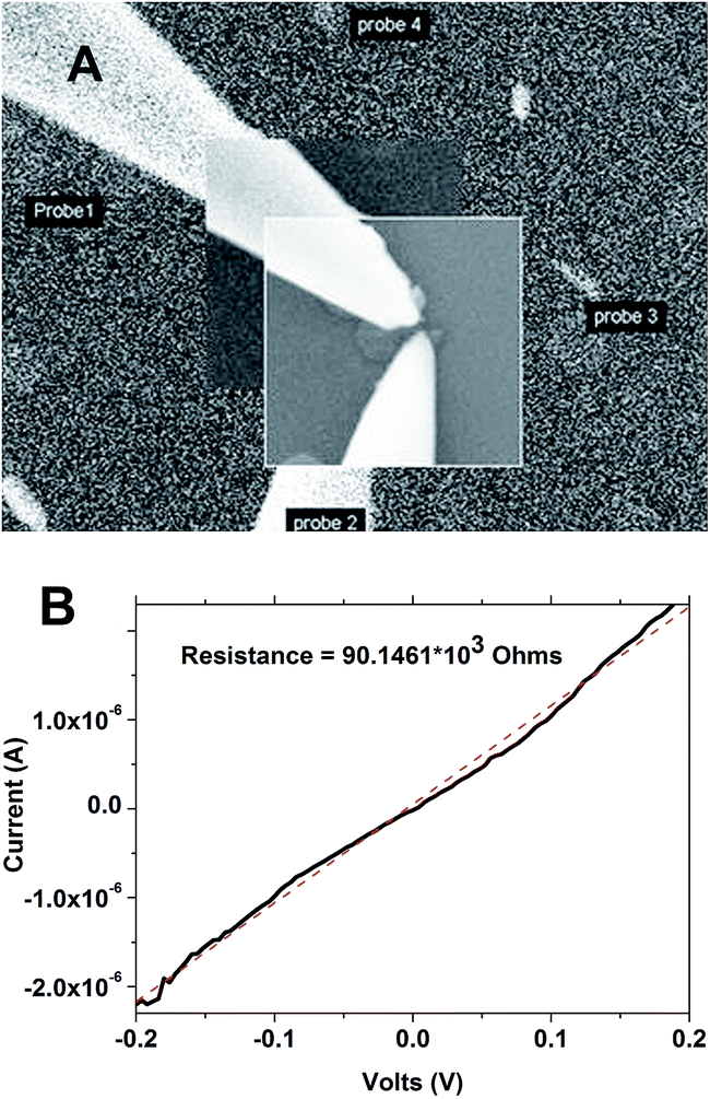 | ||
| Fig. 5 (A) Low-magnification TEM image showing the contact probes down to the single-QL Sb2Te3 NP in the electrical testing. (B) Measured current–voltage characteristics of the single-QL Sb2Te3 NP. | ||
Conclusions
In summary, we demonstrated a rational growth of high-density two-dimensional Sb2Te3 NPs with variable physical thickness through a vapor–solid process. The thickness control of the synthesized Sb2Te3 NPs down to a single-quintuple-layer was proved to be possible. The Sb2Te3 NPs are in a highly crystalline phase, covering the surface of the SiO2/Si substrate. The 2D TI nanostructures with an ultra-large surface-to-volume ratio could serve as the ideal material platform for studying surface-state conducting behaviour and the possible realization of ultra-low-dissipative electronics.Acknowledgements
The research work was partially supported by the National Science Foundation (grant no. 1162312 and 1434689).References
- E. Roduner, Chem. Soc. Rev., 2006, 35, 583–592 RSC.
- K. Novoselov, A. K. Geim, S. Morozov, D. Jiang, M. K. I. Grigorieva, S. Dubonos and A. Firsov, Nature, 2005, 438, 197–200 CrossRef CAS PubMed.
- K. S. Novoselov, Z. Jiang, Y. Zhang, S. Morozov, H. Stormer, U. Zeitler, J. Maan, G. Boebinger, P. Kim and A. Geim, Science, 2007, 315, 1379 CrossRef CAS PubMed.
- K. S. Novoselov, A. K. Geim, S. Morozov, D. Jiang, Y. Zhang, S. Dubonos, I. Grigorieva and A. Firsov, Science, 2004, 306, 666–669 CrossRef CAS PubMed.
- Y. H. Lee, X. Q. Zhang, W. Zhang, M. T. Chang, C. T. Lin, K. D. Chang, Y. C. Yu, J. T. W. Wang, C. S. Chang and L. J. Li, Adv. Mater., 2012, 24, 2320–2325 CrossRef CAS PubMed.
- K. K. Kim, A. Hsu, X. Jia, S. M. Kim, Y. Shi, M. Dresselhaus, T. Palacios and J. Kong, ACS Nano, 2012, 6, 8583–8590 CrossRef CAS PubMed.
- K. K. Kim, A. Hsu, X. Jia, S. M. Kim, Y. Shi, M. Hofmann, D. Nezich, J. F. Rodriguez-Nieva, M. Dresselhaus, T. Palacios and J. Kong, Nano Lett., 2012, 12, 161–166 CrossRef PubMed.
- B. Radisavljevic, A. Radenovic, J. Brivio, V. Giacometti and A. Kis, Nat. Nanotechnol., 2011, 6, 147–150 CrossRef CAS PubMed.
- R. B. Jacobs-Gedrim, M. Shanmugam, N. Jain, C. A. Durcan, M. T. Murphy, T. M. Murray, R. J. Matyi, R. L. Moore and B. Yu, ACS Nano, 2013, 8, 514–521 CrossRef PubMed.
- D. C. Elias, R. R. Nair, T. M. Mohiuddin, S. V. Morozov, P. Blake, M. P. Halsall, A. C. Ferrari, D. W. Boukhvalov, M. I. Katsnelson, A. K. Geim and K. S. Novoselov, Science, 2009, 323, 610–613 CrossRef CAS PubMed.
- D. Hsieh, D. Qian, L. Wray, Y. Xia, Y. S. Hor, R. Cava and M. Z. Hasan, Nature, 2008, 452, 970–974 CrossRef CAS PubMed.
- D. Hsieh, Y. Xia, L. Wray, D. Qian, A. Pal, J. Dil, J. Osterwalder, F. Meier, G. Bihlmayer and C. Kane, Science, 2009, 323, 919–922 CrossRef CAS PubMed.
- P. Hosseini, C. D. Wright and H. Bhaskaran, Nature, 2014, 511, 206–211 CrossRef CAS PubMed.
- M. Z. Hasan and C. L. Kane, Rev. Mod. Phys., 2010, 82, 3045 CrossRef CAS.
- J. Checkelsky, Y. Hor, R. Cava and N. Ong, Phys. Rev. Lett., 2011, 106, 196801 CrossRef CAS.
- Q.-K. Xue, Nat. Nanotechnol., 2011, 6, 197–198 CrossRef CAS PubMed.
- H. Peng, K. Lai, D. Kong, S. Meister, Y. Chen, X.-L. Qi, S.-C. Zhang, Z.-X. Shen and Y. Cui, Nat. Mater., 2010, 9, 225–229 CAS.
- T.-C. Chiang, Surf. Sci. Rep., 2000, 39, 181–235 CrossRef CAS.
- H.-Z. Lu, W.-Y. Shan, W. Yao, Q. Niu and S.-Q. Shen, Phys. Rev. B: Condens. Matter Mater. Phys., 2010, 81, 115407 CrossRef.
- R. B. Jacobs-Gedrim, C. A. Durcan, N. Jain and B. Yu, Appl. Phys. Lett., 2012, 101, 143103 CrossRef PubMed.
- G. Wang, X. Zhu, J. Wen, X. Chen, K. He, L. Wang, X. Ma, Y. Liu, X. Dai and Z. Fang, Nano Res., 2010, 3, 874–880 CrossRef CAS PubMed.
- D. Kong, W. Dang, J. J. Cha, H. Li, S. Meister, H. Peng, Z. Liu and Y. Cui, Nano Lett., 2010, 10, 2245–2250 CrossRef CAS PubMed.
- J. Checkelsky, Y. Hor, R. Cava and N. Ong, Phys. Rev. Lett., 2011, 106, 196801 CrossRef CAS.
- S. S. Garje, D. J. Eisler, J. S. Ritch, M. Afzaal, P. O’Brien and T. Chivers, J. Am. Chem. Soc., 2006, 128, 3120–3121 CrossRef CAS PubMed.
- G. Bendt, S. Zastrow, K. Nielsch, P. S. Mandal, J. Sánchez-Barriga, O. Rader and S. Schulz, J. Mater. Chem. A, 2014, 2, 8215–8222 CAS.
- L. Zheng, X. Cheng, D. Cao, Q. Wang, Z. Wang, C. Xia, L. Shen, Y. Yu and D. Shen, RSC Adv., 2015, 5, 40007–40011 RSC.
- Y. Zhang, K. He, C.-Z. Chang, C.-L. Song, L.-L. Wang, X. Chen, J.-F. Jia, Z. Fang, X. Dai and W.-Y. Shan, Nat. Phys., 2010, 6, 584–588 CrossRef PubMed.
- G. Hao, X. Qi, G. Wang, X. Peng, S. Chang, X. Wei and J. Zhong, RSC Adv., 2012, 2, 10694–10699 RSC.
- H. Li, J. Cao, W. Zheng, Y. Chen, D. Wu, W. Dang, K. Wang, H. Peng and Z. Liu, J. Am. Chem. Soc., 2012, 134, 6132–6135 CrossRef CAS PubMed.
- Y. Y. Li, G. Wang, X. G. Zhu, M. H. Liu, C. Ye, X. Chen, Y. Y. Wang, K. He, L. L. Wang and X. C. Ma, Adv. Mater., 2010, 22, 4002–4007 CrossRef CAS PubMed.
- Y. Yan, Z.-M. Liao, Y.-B. Zhou, H.-C. Wu, Y.-Q. Bie, J.-J. Chen, J. Meng, X.-S. Wu and D.-P. Yu, Sci. Rep., 2013, 3, 1264, DOI:10.1038/srep01264.
- M. Lin, D. Wu, Y. Zhou, W. Huang, W. Jiang, W. Zheng, S. Zhao, C. Jin, Y. Guo, H. Peng and Z. Liu, J. Am. Chem. Soc., 2013, 135, 13274–13277 CrossRef CAS PubMed.
- J. S. Lee, S. Brittman, D. Yu and H. Park, J. Am. Chem. Soc., 2008, 130, 6252–6258 CrossRef CAS PubMed.
- S. Souza, C. Poffo, D. Trichês, J. De Lima, T. Grandi, A. Polian and M. Gauthier, Phys. B, 2012, 407, 3781–3789 CrossRef CAS PubMed.
- A. Vargas, S. Basak, F. Liu, B. Wang, E. Panaitescu, H. Lin, R. Markiewicz, A. Bansil and S. Kar, ACS Nano, 2014, 8, 1222–1230 CrossRef CAS PubMed.
- W. Wang, W. Wang, B. Poudel, J. Yang, D. Wang and Z. Ren, J. Am. Chem. Soc., 2005, 127, 13792–13793 CrossRef CAS PubMed.
| This journal is © The Royal Society of Chemistry 2015 |