DOI:
10.1039/C5RA02805A
(Paper)
RSC Adv., 2015,
5, 55119-55125
Accurate determination of the size distribution of Si nanocrystals from PL spectra
Received
13th February 2015
, Accepted 16th June 2015
First published on 16th June 2015
Abstract
Narrow size distribution of quantum dots (QDs) is needed for their application in photovoltaics but collection of such information is difficult. Many experiments have shown the photoluminescence (PL) spectrum of Si QDs will broaden and peak position is size dependent. However, there is still lack of quantitative analysis of such phenomenon. In this paper, a model is developed to fit the PL spectrum based on spontaneous emission and the size distribution of the QDs. With this model, we can quantitatively analyse the QD size and its distribution using the PL spectra only, saving the need of time consuming and destructive characterization methods such as transmission electron microscopy (TEM). The optical bandgap can be extracted naturally from this PL model. The size and distribution of the QD which are obtained by fitting the PL spectra are then confirmed by measurements using TEM and XRD.
Introduction
Silicon quantum dots (Si QDs) embedded in an oxide or nitride matrix is considered to be a high energy conversion efficiencies.1 Collection of size distribution information for freestanding colloidal QDs can be done by several ways, such as transmission electron microscopy (TEM) and dynamic light scattering (DLS).2,3 However, the size distribution of Si QDs embedded in a matrix is very difficult to obtain, considering their non-uniform shapes and remarkable difficulties in TEM imaging.4,5 Here we propose a method to accurately estimate the size distribution of such QDs, based on the photoluminescence (PL) study of colloidal Si QDs. The size distribution information of Si QDs from PL fitting, when compared to the statistical values from TEM imaging, shows a very good correspondence in all parameters within 95% confidence intervals. This method can be readily adapted for size distribution analysis of QDs in a solid matrix.
Results and discussion
Three different sizes of Si QD samples were investigated in this study. Their expected average diameters were 6 nm (Sample A), 4 nm (Sample B) and 2 nm (Sample C), respectively. The QDs were synthesized by a gas-phase non-thermal plasma-assisted approach and then surface processed through a liquid-phase thermal hydrosilylation reaction.6 In this method, blended gas of silane and helium (5![[thin space (1/6-em)]](https://www.rsc.org/images/entities/char_2009.gif) :95) was introduced into a customized reactor via a carrying flow of argon. Then by applying high-frequency (13.56 MHz) power to the ring electrodes in the reactor, a nonthermal plasma atmosphere was generated to host the growth of Si NPs. The size of QDs can be adjusted by changing the reactant flow rates. The nano-particles were dissolved into chloroform. The solution was drop casted and allowed to naturally spread onto both quartz and Si substrates. After drying out, the obtained films were used for PL and XRD measurements. The volume of the solution for each sample was 50 μL and the Si nano-particle concentration was 0.05 mg mL−1. TEM measurements were performed on 10 μL solution for each sample dropped onto a TEM grid. Sizes of Si QDs were confirmed using a Philips CM200 TEM operated at 200 kV. PL measurements were performed at room temperature using a semiconductor laser with 405 nm wavelength through an OD 3.5 attenuator. The full power of the laser was 25 mW before attenuation. A TE cooled silicon CCD detector operating at −30 °C was used to detect visible/near IR signals.
:95) was introduced into a customized reactor via a carrying flow of argon. Then by applying high-frequency (13.56 MHz) power to the ring electrodes in the reactor, a nonthermal plasma atmosphere was generated to host the growth of Si NPs. The size of QDs can be adjusted by changing the reactant flow rates. The nano-particles were dissolved into chloroform. The solution was drop casted and allowed to naturally spread onto both quartz and Si substrates. After drying out, the obtained films were used for PL and XRD measurements. The volume of the solution for each sample was 50 μL and the Si nano-particle concentration was 0.05 mg mL−1. TEM measurements were performed on 10 μL solution for each sample dropped onto a TEM grid. Sizes of Si QDs were confirmed using a Philips CM200 TEM operated at 200 kV. PL measurements were performed at room temperature using a semiconductor laser with 405 nm wavelength through an OD 3.5 attenuator. The full power of the laser was 25 mW before attenuation. A TE cooled silicon CCD detector operating at −30 °C was used to detect visible/near IR signals.
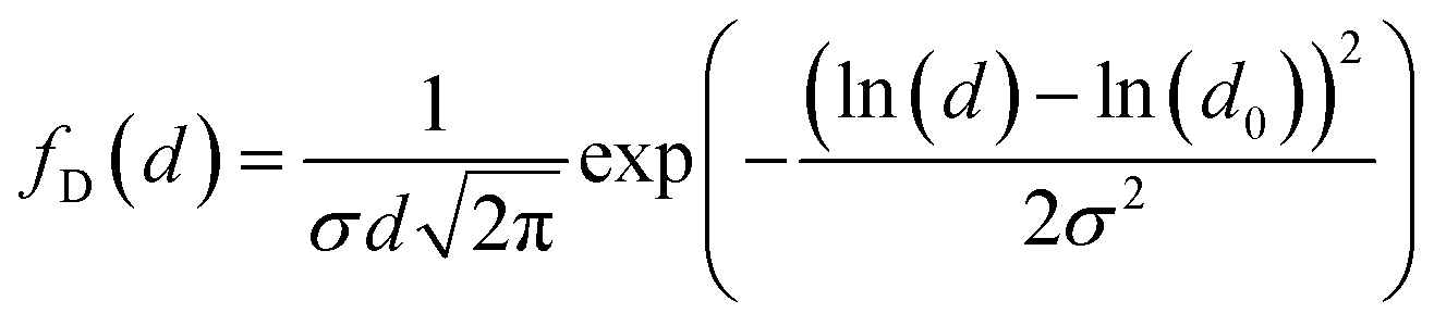
Fig. 1 shows the TEM of the Si QD samples. The QDs are clearly separated from each other. For the 4 nm sample and 6 nm sample, 200 particles are counted directly from TEM images using ImageJ. Only 45 particles are counted for the 2 nm sample due to limitations imposed by the resolution. Fig. 2 shows size distribution histograms of these samples. The nanoparticle size distribution is often reported to be log-normal and the samples under investigation in this study are also found to follow the trend.7,8 The distributions here are fitted using a log-normal function:
| |
 | (1) |
where
d0 is the geometric mean and
σ is the geometric standard deviation of the QD diameter.
 |
| | Fig. 1 TEM cross-section micrograph (a) Sample A, QD dia. ∼6 nm (b) Sample B, QD dia. ∼4 nm (c) Sample C, QD dia. ∼2 nm. | |
 |
| | Fig. 2 Size distribution histogram and its log-normal fitting curve: (a) Sample A, d0 = 6.1 nm, σ = 0.20; (b) Sample B, d0 = 3.7 nm, σ = 0.17; (c) Sample C, d0 = 2.3 nm, σ = 0.18. | |
Table 1 shows log-normal fitting values and their fitting goodness. Sample A and Sample B are fitted well by a log-normal function with a coefficient of determination R2 greater than 0.92. For Sample C, R2 is not as good with an R2 = 0.8364. One possible reason for the lower R2 is that the number of particles counted is not enough for Sample C.
Table 1 Log-normal fitting parameters for the distribution histograms
| Sample |
Best fit values |
Fitting goodness |
95% confidence intervals |
| d0 (nm) |
σ (nm) |
R2 |
d0 (nm) |
σ |
| A |
6.1 |
0.20 |
0.9436 |
5.89 to 6.22 |
0.17 to 0.23 |
| B |
3.7 |
0.17 |
0.9247 |
3.64 to 3.82 |
0.15 to 0.20 |
| C |
2.3 |
0.18 |
0.8364 |
2.16 to 2.40 |
0.14 to 0.24 |
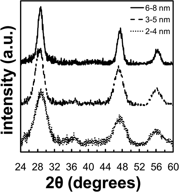
The sizes of QDs are also confirmed by glancing incidence X-ray diffraction (GIXRD) spectra (Fig. 3). The expected Si crystalline Bragg peaks are clearly visible at 28.4°, 47.4°, and 56.3°. The average grain size (L) of the QDs is estimated by Scherrer's formula:9
| |
 | (2) |
where
λ is the wavelength of the X-ray,
K is the shape factor which depends on the specific shape and size distribution of the crystalline clusters and
β is the line broadening at half the maximum intensity (FWHM). In this work, we adopt the typical value of 0.9 for the shape factor
K.
10 The effect of stress is assumed to be negligible. Crystallite sizes as per Scherrer broadening are 6.0 nm, 3.7 nm and 2.6 nm and respectively, for Samples A, B and C. Scherrer broadening size
L is the length of columns of cubic cells aligned perpendicular to the set of diffracting lattice planes, which is the minimum size of the crystallite. The maximum corresponding size is that of a spherically shaped, crystal with a diameter (
d) given by:
11| |
 | (3) |
 |
| | Fig. 3 X-ray diffraction patterns of Si QD samples, according Scherrer equation, crystallite sizes are 2–4 nm (Sample C), 3–5 nm (Sample B) and 6–8 nm (Sample C) respectively. | |
The crystal sizes of spherical particle shapes are 8.0 nm, 4.9 nm and 3.5 nm, respectively. The actual QD sizes, which are between Scherrer broadening and spherical shape, correspond fairly with the TEM results. The difference between XRD estimation and TEM measurement are 14.7%, 13.1% and 30.1% respectively, for Sample A, B and C.
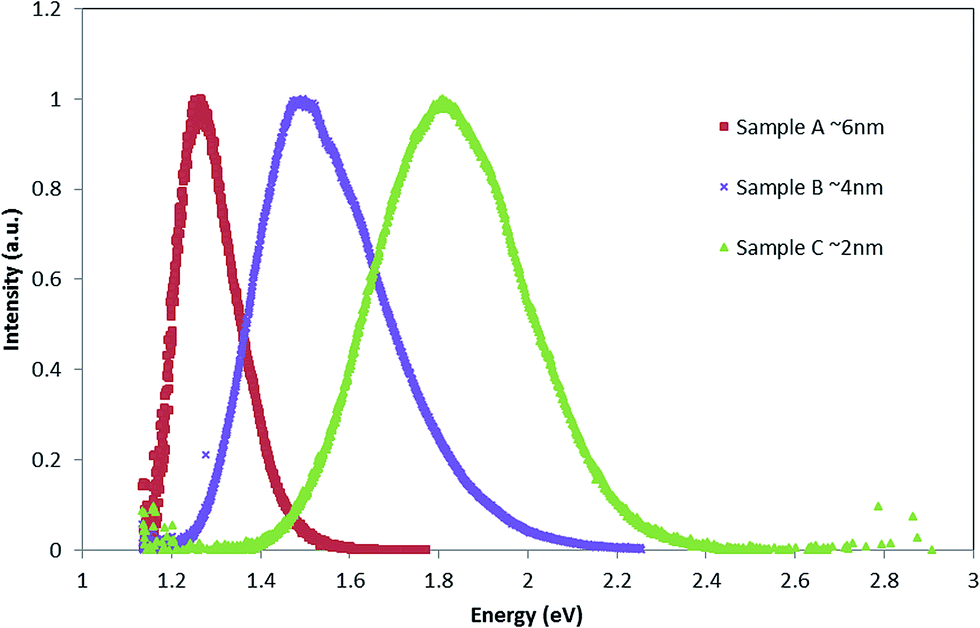
PL studies have demonstrated the tunability of the emission peak from silicon nanoparticles under optical excitation, which is explained by the quantum confinement model.12,13 Fig. 4 shows the PL spectra of the samples. It can be seen that the peak position of PL has an obvious blue shift as the dot sizes decreases. The observed breadth of the PL decreases as the particle size increases; this can be explained by the size distribution of the dots as explained below.
 |
| | Fig. 4 PL spectra of Si QD materials with different dot sizes. | |
To derive an expression explaining the shape and position of the PL emission spectra we start our model considering the radiative transition process in semiconductors. The electron transition probability from a higher energy state a to a lower energy state b can be written as:14
| | |
Rab = Rstimulated + Rspontaneous
| (4) |
where
Rstimulated is the stimulated transition probability at excitation energy
I(
ω) and
Rspontaneous is the spontaneous transition probability.
According to the Einstein's relations at steady state:14
| |
 | (5) |
where
Aab is the spontaneous emission coefficient and
Bab is the stimulated emission coefficient. At steady state,
| |
 | (6) |
where
k is the Boltzmann constant.
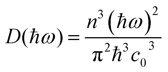
Since the lifetimes becomes longer with increasing size, at high excitation intensities emission from larger particles gets saturated quite quickly.15 This, in turn, means the contribution from the smaller particles dominates the PL, observed as a blue-shift in the PL shape. Therefore the excitation power used in this work has been reduced to the smallest achievable value (with OD 3.5 filter) in our PL setup. At room temperature, the PL emission we are interested in lies at wavelengths shorter than 2000 nm. For these wavelengths the ratio in eqn (6) is greater than 1010 showing that the PL emission is dominated by spontaneous emission. Therefore, for an emission between 200 nm and 2000 nm, we only considered the spontaneous emission:14
| |
 | (7) |
where
is the number of states per unit energy range,
n is the refractive index,
c0 is the velocity of light in vacuum.
Na,
N′
b are the electron and hole occupation number at energy level a and b respectively,
na,
n′
b is the density of states of the electron–hole pairs.

, is linked to the optical transition matrix element |〈a|
![[p with combining circumflex]](https://www.rsc.org/images/entities/i_char_0070_0302.gif)
|b〉|
2.
Before simplifying eqn (7), we need to prove that the semiconductor is still non-degenerated under illumination. It is assumed here that the absorption coefficient α at 408 nm wavelength is around 1 × 105 cm−1 according to the transmission and reflection measurements of these samples at this wavelength. A long minority carrier life time τ = 1 μs is assumed.16 The laser power after attenuation is 2.5 × 10⁻⁵ W at 408 nm wavelength, so the photon flux F coming into the sample is around 5 × 10¹³ # cm−2. The thickness of the sample (d) is around 10 nm. To obtain the largest photon generation, it is assumed all photons are absorbed. The average carrier generation rate across the whole sample is:
| |
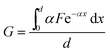 | (8) |
Substituting all the estimated values into eqn (8), we can obtain the average carrier generation rate is around 3 × 1018 cm−3. Thus, the excess photon generated carrier is Δn = Δp = Gτ = 3 × 1012 cm−3. If we assume the intrinsic carrier concentration in this material is still 1 × 1010 cm−3 at room temperature, the carrier concentration will be n ≈ Δn = 3 × 1012 cm−3. Thus, the split between electron quasi Fermi energy EFn and intrinsic Fermi energy Ei can be extracted from:
| |
 | (9) |
Based on the same calculation for hole concentration, we can obtain EFn − Ei = Ei − EFp ≈ 0.147 eV. The intrinsic Fermi energy Ei locates near the mid of the band, which means EC − Ei ≈ Ei − EV ≥ 0.55 eV. Thus, EC − EFn ≈ EFp − EV ≫ 3kT, the semiconductor is still non-degenerated under this illumination.
In a non-degenerated semiconductor, parabolic bands are assumed in the vicinity of conduction band minima and valence band maxima, as the radiative transitions mainly occur between them. The emission probability is proportional to the states occupied by electrons at Ea which is  and the states not occupied by electrons at Eb which is
  . Applying eqn (7), we can obtain:
| |
 | (10) |
EFn and
EFp are quasi-Fermi energy level of electrons and holes.
Jcv is the joint density states, which is the integration over all pairs of states in the valence and conduction bands. With the parabolic band approximation,
Jcv is proportional to (
ħω −
Eg)
W.
17 W depends on whether the transition process is direct (
W = 0.5) or indirect (
W = 2).
17,18 In the case of nanocrystal silicon, some reports indicate that this transition can still be regarded as that of an indirect bandgap material.
19,20 Hence
W = 2 is assumed here. The equation can be simplified by replacing the Fermi–Dirac distribution by the Boltzmann distribution because the material is non-degenerate. If we consider the distribution of bandgap caused by particle size distribution, the expression for the emission probability can be written as:
| |
 | (11) |
where Δ
F =
EFn −
EFp is a constant,
fEg(
Eg) is the probability density function (PDF) of the bandgap. Since we adopted a log-normal size distribution for nanoparticles, the bandgap distribution function can be obtained as explained below.
Considering quantum confinement, the ground state energy in a silicon quantum dot according to effective mass approach (EMA) is:21,22
| |
 | (12) |
where
Eg_bulk is the bandgap of bulk silicon,
R is the radius of the silicon quantum dot,
me and
mh are effective masses of electron and hole respectively, the last term is the energy shifts as a result of quantum localization of electrons and holes (quantum confinement).
Eqn (12) can be written as:13
| |
 | (13) |
where
Eg_bulk is the bandgap of the bulk material,
d is the diameter of nanocrystals and
Clump is a coefficient lumping all other parameters. This value is not a universal constant and seems to depend on the details of the Si QD fabrication with different groups reporting different bandgaps for the same QD size.
1,23–26 This is because in the EMA calculation, the crystal potential which depends on both Si and dielectric matrix has been included in the effective mass
m*. Therefore, for the Si QD embedded in different dielectric,
m* will be different, which leads to the difference of confinement effect for different dielectric matrix. Here we use
Clump = 3 eV nm
2 as this corresponds well with the results obtained from our work.
From eqn (1) and (13), the distribution of bandgap is:
| |
 | (14) |
where
FEg and
FD are cumulative distribution function of d and
Eg, respectively.
The weighted average is then given by:
| |
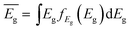 | (15) |
Using eqn (11) and (14), we can fit the PL spectrum by adjusting d0 and σ. The best fits are shown in Fig. 5. Table 2 shows that the QD sizes and the deviation are in good agreement with the measurements from TEM images and the values of all the fitting parameters from PL fall within the 95% confidence intervals.
 |
| | Fig. 5 (a) Experimental PL data Sample A, (b) experimental PL data of Sample B, (c) experimental PL data of Sample C, (d) simulated PL with log-normal size distribution of Sample C (d0 = 2.2 nm, σ = 0.13), (e) simulated PL with log-normal size distribution of Sample B (d0 = 3.7 nm, σ = 0.20), (f) simulated PL with log-normal size distribution of Sample C (d0 = 6.2 nm, σ = 0.25). | |
Table 2 Comparison of the log-normal function fitting parameters from TEM and PL
| Sample |
Fit values from TEM |
Fit values from PL |
| d0 (nm) |
σ |
d0 (nm) |
σ |
| A |
6.1 |
0.20 |
6.2 |
0.25 |
| B |
3.7 |
0.17 |
3.7 |
0.20 |
| C |
2.3 |
0.18 |
2.2 |
0.13 |
Fig. 5 shows that the simulated PL spectra can fit the experimental data closely. Then the size distribution can be easily determined by plotting the probability density function of the size using the geometric mean and standard deviation. The PDF for each sample obtained from the PL spectra fitting is compared to the PDF based on the TEM size distribution analysis, which is shown in Fig. 6. The difference between the fitting from PL and TEM is acceptable as the values of all the fitting parameter from PL falls within the 95% confidence intervals of fitting from TEM. It can be seen that this model predicts the blue-shift of the PL peak correctly, which agrees with the explanation with quantum confinement effect. It also agrees with the broadening and skewness of the experimental spectrum.
 |
| | Fig. 6 Size distribution histogram and its log-normal fitting curve from TEM and PL with parameters in Table 2: (a) Sample A; (b) Sample B; (c) Sample C. | |
Many studies which aimed at extracting the optical bandgap of Si QD materials modified from that of the bulk due to quantum confinement used the widely accepted Tauc-plot method.27–29 However, even in these cases, the Tauc plot with γ = 1/2 does not show a strict linearity. Some reports point out that silicon nanoparticles do not follow the simple Tauc relation, resulting in an uncertainty when extracting the optical bandgap of Si nanoparticle from this simple method.18,30 The peak position of the PL emission is another common method to estimate optical bandgap of Si QD materials. But as can be seen from the model presented here, the peak position of the PL is not the actual optical bandgap. For bulk materials such as Si for which excitons do not play a big role in the emission or absorption of light, the PL emission intensity increases sharply at the bandgap and reaches a maximum within 0.01 eV, so that the peak position can be safely regarded as the bandgap.19 The PL peak is, therefore, a good indicator for the bandgap energy.
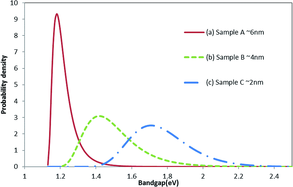
However, for silicon QDs, the particle size distribution will broaden the PL spectrum and there is no definite bandgap but rather a distribution of bandgaps. Fig. 7 shows that the distribution of bandgap will broaden when Si QD size is reduced for a given geometric standard deviation. This can explain the observed PL broadening and higher energy skewness as the particle size decreases. Table 3 shows the comparison of the PL peak position, weighted average bandgap and the smallest bandgap obtained from Fig. 7. We can obtain the weighted average bandgap from eqn (13) which is close to the PL peak position by 0.1 eV. The absorption edge, on the other hand, should start from the smallest bandgap extracted, which means the effective optical bandgap may be determined by the largest QD rather than the average size in this material. By fitting the PL spectrum, we can obtain the bandgap distribution and thereby obtaining the smallest bandgap which may be a better indicator of effective optical bandgap compared with the PL peak position in a material with a given size distribution.
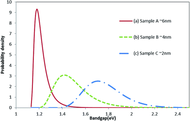 |
| | Fig. 7 (a) Simulated bandgap distribution of Sample A (d0 = 6.2 nm, σ = 0.25, C = 3 eV nm2); (b) simulated band-gap distribution of Sample B (d0 = 3.7 nm, σ = 0.20, C = 3 eV nm2); (c) simulated band-gap distribution of Sample C (d0 = 2.2 nm, σ = 0.13, C = 3 eV nm2). | |
Table 3 Comparison of the PL peak position, mean bandgap and the smallest bandgap
| Sample |
PL peak position (eV) |
Mean bandgap (eV) |
Smallest bandgap (eV) |
| A |
1.26 |
1.18 |
1.14 |
| B |
1.50 |
1.41 |
1.22 |
| C |
1.79 |
1.73 |
1.41 |
Conclusion
In this work, we analysed the PL spectrum of Si nano-particles quantitatively and extracted the size distribution information in Si QD materials from PL study. We calculated the emission probability and developed a model to simulate the PL spectrum by inducing the distribution of QD sizes that in turn causes a distribution of the bandgap. The model demonstrates that the PL peak position is a good indicator of the mean optical bandgap but may not be a good indicator of the effective bandgap. The model is flexible enough to be used to analyse the PL spectrum of other type nanoparticles by adjusting the joint density of states and size distribution.
Acknowledgements
This Program has been supported by the Australian Government through the Australian Renewable Energy Agency (ARENA). Responsibility for the views, information or advice expressed herein is not accepted by the Australian Government.
References
- G. Conibeer, M. Green, E. Cho, D. Konig, Y. Cho, T. Fangsuwannarak, G. Scardera, E. Pink, Y. Huang and T. Puzzer, Thin Solid Films, 2008, 516(20), 6748–6756 CrossRef CAS PubMed.
- H. Borchert, E. V. Shevchenko, A. Robert, I. Mekis, A. Kornowski, G. Grübel and H. Weller, Langmuir, 2005, 21(5), 1931–1936 CrossRef CAS PubMed.
- T. T. Tan, S. T. Selvan, L. Zhao, S. Gao and J. Y. Ying, Chem. Mater., 2007, 19(13), 3112–3117 CrossRef CAS.
- M. Zacharias, J. Heitmann, R. Scholz, U. Kahler, M. Schmidt and J. Bläsing, Appl. Phys. Lett., 2002, 80(4), 661–663 CrossRef CAS PubMed.
- L. F. Kourkoutis, X. Hao, S. Huang, B. Puthen-Veettil, G. Conibeer, M. A. Green and I. Perez-Wurfl, Nanoscale, 2013, 5(16), 7499–7504 RSC.
- R. J. Anthony, D. J. Rowe, M. Stein, J. Yang and U. Kortshagen, Adv. Funct. Mater., 2011, 21(21), 4042–4046 CrossRef CAS PubMed.
- L. B. Kiss, J. Söderlund, G. A. Niklasson and C. G. Granqvist, Nanotechnology, 1999, 10(1), 25 CrossRef.
- J. Söderlund, L. B. Kiss, G. A. Niklasson and C. G. Granqvist, Phys. Rev. Lett., 1998, 80(11), 2386–2388 CrossRef.
- S. Hasegawa, S. Watanabe, T. Inokuma and Y. Kurata, J. Appl. Phys., 1995, 77(5), 1938–1947 CrossRef CAS PubMed.
- A. L. Patterson, Phys. Rev., 1939, 56(10), 978–982 CrossRef CAS.
- H. Natter, M. Schmelzer, M. S. Löffler, C. E. Krill, A. Fitch and R. Hempelmann, J. Phys. Chem. B, 2000, 104(11), 2467–2476 CrossRef CAS.
- A. G. Cullis, L. T. Canham and P. D. J. Calcott, J. Appl. Phys., 1997, 82(3), 909–965 CrossRef CAS PubMed.
- D. Di, I. Perez-Wurfl, G. Conibeer and M. A. Green, Sol. Energy Mater. Sol. Cells, 2010, 94(12), 2238–2243 CrossRef CAS PubMed.
- M. F. Li, Modern Semiconductor Quantum Physics, World Scientific Publishing Company, Incorporated, 1995 Search PubMed.
- S. Takeoka, M. Fujii and S. Hayashi, Phys. Rev. B: Condens. Matter Mater. Phys., 2000, 62(24), 16820–16825 CrossRef CAS.
- M. D. Kelzenberg, D. B. Turner-Evans, B. M. Kayes, M. A. Filler, M. C. Putnam, N. S. Lewis and H. A. Atwater, Nano Lett., 2008, 8(2), 710–714 CrossRef CAS PubMed.
- J. Tauc, R. Grigorovici and A. Vancu, Phys. Status Solidi B, 1966, 15(2), 627–637 CrossRef CAS PubMed.
- S. Datta and K. L. Narasimhan, Phys. Rev. B: Condens. Matter Mater. Phys., 1999, 60(11), 8246–8252 CrossRef CAS.
- D. Kovalev, H. Heckler, G. Polisski and F. Koch, Phys. Status Solidi B, 1999, 215(2), 871–932 CrossRef CAS.
- D. Kovalev, J. Diener, H. Heckler, G. Polisski, N. Künzner and F. Koch, Phys. Rev. B: Condens. Matter Mater. Phys., 2000, 61(7), 4485–4487 CrossRef CAS.
- P. Harrison, Quantum Wells, Wires and Dots: Theoretical and Computational Physics of Semiconductor Nanostructures. Wiley, 2011 Search PubMed.
- M. A. Green, J. Appl. Phys., 1990, 67(6), 2944–2954 CrossRef CAS PubMed.
- A. J. Read, R. J. Needs, K. J. Nash, L. T. Canham, P. D. J. Calcott and A. Qteish, Phys. Rev. Lett., 1992, 69(8), 1232–1235 CrossRef CAS.
- D. Kovalev, H. Heckler, M. Ben-Chorin, G. Polisski, M. Schwartzkopff and F. Koch, Phys. Rev. Lett., 1998, 81(13), 2803–2806 CrossRef CAS.
- H. Takagi, H. Ogawa, Y. Yamazaki, A. Ishizaki and T. Nakagiri, Appl. Phys. Lett., 1990, 56(24), 2379–2380 CrossRef CAS PubMed.
- T. van Buuren, L. N. Dinh, L. L. Chase, W. J. Siekhaus and L. J. Terminello, Phys. Rev. Lett., 1998, 80(17), 3803–3806 CrossRef CAS.
- C.-H. Huang, X.-Y. Wang, M. Igarashi, A. Murayama, Y. Okada, I. Yamashita and S. Samukawa, Nanotechnology, 2011, 22(10), 105301 CrossRef PubMed.
- J. K. Choi, S. Jang, H. Sohn and H. D. Jeong, J. Am. Chem. Soc., 2009, 131(49), 17894–17900 CrossRef CAS PubMed.
- X. J. Hao, E. C. Cho, C. Flynn, Y. S. Shen, G. Conibeer and M. A. Green, Nanotechnology, 2008, 19(42), 424019 CrossRef CAS PubMed.
- B. G. Lee, D. Hiller, J.-W. Luo, O. E. Semonin, M. C. Beard, M. Zacharias and P. Stradins, Adv. Funct. Mater., 2012, 22(15), 3223–3232 CrossRef CAS PubMed.
Footnote |
| † Present address: Michigan State University, Engineering Building 428 S, Shaw Lane East Lansing, MI 48824-1226, USA. |
|
| This journal is © The Royal Society of Chemistry 2015 |
Click here to see how this site uses Cookies. View our privacy policy here. 


 is the number of states per unit energy range, n is the refractive index, c0 is the velocity of light in vacuum. Na, N′b are the electron and hole occupation number at energy level a and b respectively, na, n′b is the density of states of the electron–hole pairs.
  , is linked to the optical transition matrix element |〈a|

 and the states not occupied by electrons at Eb which is
 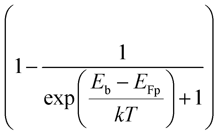 . Applying eqn (7), we can obtain: