Enhanced photocatalytic activities of Bi2WO6 by introducing Zn to replace Bi lattice sites: a first-principles study

Fengzhu Rena, Jihua Zhangb and Yuanxu Wang*a
aInstitute of Computational Materials Science, School of Physics and Electronics, Henan University, Kaifeng 475004, People’s Republic of China. E-mail: wangyx@henu.edu.cn; Fax: +86-0371-23889990; Tel: +86-0371-23889990
bGuizhou Provincial Key Laboratory of Computational Nano-Material Science, Guizhou Normal College, Guiyang 550018, People’s Republic of China

Received 12th February 2015 , Accepted 16th March 2015

First published on 16th March 2015


Abstract

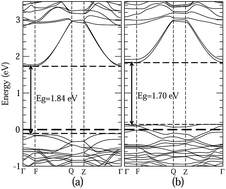
The geometry structure, electronic structure, and band edge positions of Zn-doped Bi2WO6 have been studied using a first-principles method. Bi1.75Zn0.25WO6 has a high quantum efficiency (QE) caused by the large mobility along different orientations and the efficient photogenerated-electron trap. It exhibits an enhanced visible-light absorption capability (α) due to the large increase of the density of electrons in the valence band maximum (VBM) and decrease in the band gap. The interactions are both strengthened between layers and among atoms within (Bi2O2)n layers. These strengthened interactions induce an enhanced stereochemically active Bi lone pair effect, which is identified as the cause of its unique electronic structure. Furthermore, the valence band (VB) and conduction band (CB) edges of Zn-doped Bi2WO6 are slightly shifted upwards. This indicates that the dominant active species during photocatalytic reaction for Bi1.75Zn0.25WO6 are not only hole and electron but also ˙O2 ion and ˙OH radical.


I. Introduction

Since the discovery of photocatalytic hydrogen production by the splitting of water on TiO2 electrodes by Fujishima and Honda in 1972,1 the artificial photosynthesis or photocatalytic process has been considered to be a promising technique for solving many current energy and environmental issues. TiO2 has been studied extensively in the field of photocatalysis owing to its nontoxicity, low cost, chemical inertness, and availability. Moreover, it has been proven that TiO2 is the most suitable photocatalytic material among various oxide and nonoxide semiconductor photocatalysts.2–4 Unfortunately, because of its wide band gap (3.2 eV for anatase and 3.0 eV for rutile), TiO2 can be only activated under ultraviolet (UV) irradiation, which is a small portion of the solar spectrum (containing about 4% UV light and 43% visible light). This prevents its practical applications.

Up to now, great efforts have been made to develop new photocatalysts. One way is the surface modification of TiO2 with co-catalysts or bulk doped TiO2 to extend its absorption in the visible range and improve its quantum efficiency (QE). Another emerging desirable approach is to find new photocatalysis materials that absorb in the visible range.5 Bismuth-based oxides are good candidates due to their visible-light absorption band. It has been highlighted that visible-light absorption comes from the transition from filled anti-bonding states, formed by the hybrid of Bi 6s and O 2p at the top of the valence band to the corresponding conduction band.6–10 Moreover, these bismuth-based oxides are chemically and thermally stable and nontoxic.11 Among them, Bi2WO6 seems to be one of the more efficient photocatalysts.12 However, the band gap of Bi2WO6 is still too large to realize a sufficiently large absorption of the solar spectrum. Much effort has been devoted to improve the visible-light absorptivity and catalytic activities of Bi2WO6 by controlling the preparation process, sensitizing with organic dyes, and constructing heterojunction interfaces.13–31 But the photocatalytic activity of Bi2WO6 is relatively low in comparison with TiO2.32 Firstly, the low light absorption capability (α) of Bi2WO6 results in low photon harvesting efficiency. Secondly, it has a low conversion of the generated holes and electrons in active radicals, which may be related to the rapid recombining of its photogenerated electron–hole pairs and unsuitable conduction band position. Therefore, it is desirable to improve its photocatalytic activity by modifying its band structure.

Doping is also a possible way to tailor the band structure of photocatalysts to shift the absorption edge towards long-wave and place its band edges at proper positions, thus improving its photocatalytic efficiency. For example, previous studies have shown that doping TiO2 leads to an effective band-gap narrowing and some visible-light catalytic activity.33,34 However, experimental studies also show that for many kinds of doping, the photogenerated current is low due to the partially occupied impurity bands, which can act as recombination centers and reduce the photogenerated current or form strongly localized states, significantly reducing the carrier mobility.35,36 Zn is a good dopant because Zn2+ will enable the merging and coupling of the highest occupied dopant states into the valence band (VB) to raise its energy and reduce the band gap. In particular, a Zn dopant will not introduce deep impurity levels in the forbidden band of semiconductor photocatalysts, where they act as a recombination center and impair photocatalytic activity thanks to its stable d10 electronic configuration and low electronegativity. In addition, the smaller ionic radii of Zn2+ (0.70 Å) compared to that of Bi3+ (1.03 Å) will lead to a distortion of the crystal structure. Mohn et al. showed that the lone pair of bismuth is stereochemically active in Bi2WO6.37 According to the revised lone pair (RLP) theory,38 a stereochemically active bismuth lone pair structure will be enhanced by distorting the crystal structure, which is meaningful from aspects of physics and applications. Furthermore, Bi2WO6 is a simple Aurivillius oxide with alternating layers of (Bi2O2)n and (WO6)n, which can promote the efficient separation of electron hole pairs. Therefore, Zn-doped Bi2WO6 may exhibit high visible-light photocatalytic reaction rate determined by the multiplication of visible-light α and QE. In this work, we systematically investigate the geometry structure, and electronic properties of pure and Zn-doped Bi2WO6 using standard generalized gradient approximation (GGA) based on the density functional theory (DFT) calculation. This study will provide new insights into understanding the mechanism of photocatalytic activity and allow the design of new photocatalytic materials with the required electronic properties.

II. Computational method

All calculations were performed using DFT, using the projector-augmented wave (PAW) pseudopotential method.39 We use the Vienna ab initio simulation package (VASP),40,41 which implements the method. The GGA42 in the scheme of Perdew–Burke–Ernzerhof (PBE)43 is used for the exchange-correlation functional. We have tested the total energy convergence with respect to the plane-wave energy cutoff. In order to obtain more accurate results, we used a kinetic energy cutoff of 400 eV. Several convergence tests in the k-point sampling were performed, and a Monkhorst–Pack k-point mesh of 5 × 3 × 5 was used for geometry optimization and electronic property calculations, which is found to be sufficient to reach convergence for bulk calculations. The explicit inclusion of the outer core d shells of the bismuth (the 5d states) and the 5p core shells on the tungsten have a very little effect on lattice parameters, bond lengths, and bond angles.44,45 The PAW potentials with the valence states 6s6p for Bi, 2s2p for O, 5d6s for W, and 3d4s for Zn, have been employed. The stopping criterion for electronic self-consistent interactions demonstrates convergence of the total energy to within 10−7 eV. The calculations were performed with relaxation of both atomic positions and lattice parameters to find the most stable lattice structure. The structure is considered to be in equilibrium as the Hellmann–Feynman forces on each ions are less than 0.02 eV Å−1.

We build up our Bi2WO6 initial computational model according to the experimental lattice parameters and the atomic positions as starting points. Under normal conditions, Bi2WO6 crystallizes to form an orthorhombic crystal system with a space group of Pca2(1), no. 29, lattice constants of a = 5.4326 Å, b = 16.4302 Å, c = 5.4584 Å.46 The optimized structural parameters are listed in Table 1. From this table, it can be seen that our calculated equilibrium lattice parameters are in excellent agreement with the experimental results. To simulate the variational Zn-doped Bi2WO6 models, different sizes of Bi2WO6 supercells were used, in which some Bi atoms were substituted by Zn atoms, The Zn impurity concentrations, of about 6.25% (Bi1.875Zn0.125WO6), 12.5% (Bi1.75Zn0.25WO6), and 25% (Bi1.5Zn0.5WO6), correspond to one Bi atom, one Bi atom, and two Bi atoms substituted by one Zn atom, one Zn atom, and two Zn atoms in 72-atom, 36-atom, and 36-atom Bi2WO6 supercells, respectively. The geometry optimizations were performed for nonequivalent Bi atoms substituted by Zn to find the appropriate doping site.

Table 1 Equilibrium lattice constants (in Å), equilibrium volume V0 (in Å3 per unit), and band gap (in eV) for Bi2WO6 and Bi1.75Zn0.25WO6 compared with the experimental results
  Lattice constants Volume V0 Band gap Eg
a b c
a Ref. 46.b Ref. 51.
Bi2WO6-expt.a 5.4326 16.4302 5.4584 487.21 2.80b
Bi2WO6-present 5.4255 16.3967 5.4255 483.73 1.84
Bi1.75Zn0.25WO6 5.4149 16.2926 5.4052 476.78 1.70


The different ways of doping generate different lattice distortions, which make the doped Bi2WO6 having different properties. In order to determine whether substituting Zn for Bi lattice sites is more-favorable energetically, the formation energies (Eform) of doped-Bi2WO6 were calculated. The Eform is calculated by following formula:

 
Eform = EdopedEpureEBi + EZn, (1)
 
Eform = EdopedEpureEW + EZn, (2)
where Edoped and Epure are the total energy of the pure and doped-Bi2WO6. EBi, EW, and EZn are the total energy of per atom for Bi-hexagonal, W-cubic, and Zn-hexagonal solids, respectively. The calculated formation energies for Bi1.75Zn0.25WO6 (7.22 eV) are lower than that of Bi2Zn0.25W0.75O6 (8.45 eV). This confirms that Zn prefers to occupy Bi sites rather than W sites for Zn-doped Bi2WO6, which is in agreement with the X-ray photoelectron spectroscopy (XPS) result.47

III. Results and discussion

A. Geometry structures

The calculated total energies are equivalent when substituting Zn for nonequivalent sites of Bi. Here we use substituting Zn for Bi(I). The optimized stable configurations of Bi2WO6 and Bi1.75Zn0.25WO6 are illustrated in Fig. 1. As seen in Fig. 1(a), Bi2WO6 is structurally composed of alternating perovskite-like (WO4)n2− slabs connected to each other by corner-sharing and fluorite-like (Bi2O2)n2+ layers. The unique structure is in the common possession of bismuth-based mixed oxides with the Aurivillius structure represented by (Bi2O2)n2+ [Am−1BmO3m+1]n2− (A = Ba, Bi, Pb, etc., B = Ti, Nb, W, Mo, etc., for Bi2WO6, A = Bi, B = W, and m = 1). Each Bi atom is bonded to four oxygen O(III) atoms within (Bi2O2)n layers arranged in a flat square. All four coordinated oxygen atoms with bismuth are found on the side of the corresponding Bi. In corner-sharing of the WO6 octahedra, the bond angles of ∠W–O–W are approximately 102, 150, and 161°, and W–O bond-lengths are 1.82, 1.82, 2.14, 2.15, 1.88, and 1.88 Å, which suggests that Bi2WO6 holds a distorted WO6 octahedron. Moreover, the (101), (10[1 with combining macron]), (100), and (001) planes are mainly composed of cations, Bi and W, while (010) planes have only O atoms.
image file: c5ra02735g-f1.tif
Fig. 1 Crystal structures for optimized (a) Bi2WO6 and (b) Bi1.75Zn0.25WO6. For brevity, the labeling, Bi(I) and Bi(II) refer to two types of Bi atom (green) within the Bi2O2 layers; O(I) and O(II) refer to the apex and corner-sharing oxygens (red) of the WO6 octahedra; O(III) (red) refers to the oxygens within the Bi2O2 layers; the magenta spheres for W; the blue spheres for Zn.

Fig. 1(b) shows the optimized geometry structure for Bi1.75Zn0.25WO6. Bi1.75Zn0.25WO6 maintains the structural characteristics of Bi2WO6, which possesses alternating (WO6)n slabs connected to each other by corner-sharing and (Bi1.75Zn0.25O2)n layers. Its (010) planes only contain O atoms, while (101), (10[1 with combining macron]), (100), and (001) planes contain Bi, Zn, and W atoms. However, the most striking is that the short Bi(II)–O(I) and Zn–O(I) bonds are formed among Bi(II), Zn (Bi(II) and Zn bonded with the same four O(III)), and the apex oxygen O(I) of the perovskite layer. Thus, these Bi(II), Zn atoms are tightly bonded with the neighboring five oxygen atoms, which results in the shortening of the maximum and minimum Bi(II)–O(III) and Zn–O(III) bond lengths compared with Bi2WO6. It suggests that the interaction between the (WO6)n slabs and (Bi2O2)n layers is strengthened. As shown in Table 1, the lattice constant along the b direction and cell volume of Bi1.75Zn0.25WO6 are significantly smaller than that of Bi2WO6. The interaction is a driving force for the structure distortion. This distortion changes the Bi–O and W–O bond lengths and bond angle ∠W–O–W for Bi1.75Zn0.25WO6 (not shown here). Zn2+ has a smaller ionic radius (0.70 Å) and Pauling electronegativity (1.6 eV) than that of Bi3+ (1.03 Å and 1.9 eV), which results in the atomic rearrangement and strengthening interaction. It is well known that the structure has an important effect on the electronic properties, including the band gap. Therefore, it is desirable to further investigate the electronic structures of pure and doped Bi2WO6 by substituting Zn for Bi lattice sites.

B. Electronic structures

Now we investigate the electronic structure of Bi2WO6 and Bi1.75Zn0.25WO6. The electronic localization function (ELF)48 offers a reliable measure of electron pairing and localization. The ELF values are scaled between 0 and 1, where ELF = 1 corresponds to the perfect localization characteristic of covalent bonds or lone pairs. We calculated the ELF of Bi2WO6 and Bi1.75Zn0.25WO6. Fig. 2(a) and (b) plot their ELF with the isosurface at ELF = 0.9. We can see that the Bi lone pair electron appears in the side of the Bi atom and away from Bi–O bonds. Gillespie and Nyholm noted repulsions involving lone pair induced non-symmetric crystals, where the lone pair electrons occupy the corner of a polyhedron.49 This is similar to the case of α-PbO where all four coordinated oxygen atoms were found on the side of Pb and the stereochemically active lone pairs of Pb were projected out in the opposite direction.50 Based on above discussion of the geometry and the ELF, we show that the lone pairs of Bi may be stereochemically active. To analyze the chemical bonding of Bi2WO6 and Bi1.75Zn0.25WO6, we plot their ELF in Fig. 2(c) and (d), with the isosurface at ELF = 0.60. There are ionic-bond interactions between the anion and cation Bi, W, and Zn atoms, respectively. Apart from the lone pairs of Bi, the shell electrons are both transferred from Bi, W, and Zn to O atoms.
image file: c5ra02735g-f2.tif
Fig. 2 ELF of the three-dimensional framework for (a) Bi2WO6 and (b) Bi1.75Zn0.25WO6 with the value of isosurface at ELF = 0.90. (c) Bi2WO6 and (d) Bi1.75Zn0.25WO6 with the value of isosurface at ELF = 0.60.

In order to clearly show the layered anisotropic lattice structure in reciprocal space, we plot its Brillouin zone in Fig. 3, where ΓF (ZQ) and ΓZ (FQ) correspond to b and a orientations in real space. To calculate the change of the band gap (Eg) and density of states (DOS), we align the single-particle eigenvalues of the perfect host sample and the doped sample according to the 2s core level of the oxygen atom which is the farthest away from the impurity. The calculated band structure is plotted in Fig. 4. The calculated band gap of Bi2WO6 is 1.84 eV (Fig. 4(a)), which is smaller than the experimental value, 2.8 eV,51 due to the well-known shortcoming of the exchange-correction functional in describing excited states. However, it is still a widely accepted method to determine electronic structure, and this gives reasonable explanation for the experimental results. As seen from Fig. 4(a) and (b), Bi2WO6 and Bi1.75Zn0.25WO6 are both direct band-gap semiconductors and have an anisotropic band structure (large dispersion along FQ and ZΓ, flat along QZ). The stronger interactions between Bi and O atoms in the (Bi2O2)n layers are responsible for the larger dispersion along FQ and ZΓ, while the weaker interactions between (WO6)n slabs and (Bi2O2)n layers lead to the smaller dispersion along ΓF and QZ. Compared with Bi2WO6, Fig. 4(b) shows that Zn-doping makes the conduction band minimum (CBM) and the valence band maximum (VBM) shift upwards. Moreover, Zn-doping decreases the band gap by about 0.14 eV, and makes the band flat, and the band convergence increases along ΓF and the band splits along QZ on the VBM.


image file: c5ra02735g-f3.tif
Fig. 3 The first Brillouin zone of pure and doped Bi2WO6.

image file: c5ra02735g-f4.tif
Fig. 4 Band structures of (a) Bi2WO6, (b) Bi1.75Zn0.25WO6.

By analyzing the projected density of states (PDOS) (Fig. 5), we can deeply understand the effect of Zn doping on the electronic structure. As shown in Fig. 5(a), the conduction bands (CB) are formed by W 5d, O 2p, and Bi 6p states, while the CBM is attributed dominantly to W 5d states. There are distinct Bi 6s states at the top and bottom of the valence band. Simultaneously, there is a band split off from the bottom of the O 2p valence band at −10 eV to −7 eV. The PDOS shows that the Bi 6s orbitals make the largest orbital contribution to this split-off band. However, there is a non-negligible amount of oxygen character. Therefore, this split-off band comes from Bi 6s–O 2p bonding states rather than Bi 6s nonbonding states. As we know, the bonding and antibonding interactions occur in pairs. In Bi2WO6, the filled Bi 6s–O 2p antibonding states appear on the top of the valence band. Moreover, Bi 6p states also exist on the top of the VB. In the top of the VB, the mixing of Bi 6s–O 2p–Bi 6p states stabilize the occupied Bi 6s–O 2p states near the Fermi-level (EF). Thus, the stereochemically active bismuth lone pair structure can be seen, which agrees with the description of the geometry structure given above.


image file: c5ra02735g-f5.tif
Fig. 5 The projected density of states (PDOS) of (a) Bi2WO6 and (b) Bi1.75Zn0.25WO6. The insert figures (c) Bi2WO6 and (d) Bi1.75Zn0.25WO6 are the zoomed in regions at the top of the valence band. The Fermi level (EF) of these systems is displayed with a dashed line.

For the case of Zn-doped Bi2WO6 (Bi1.75Zn0.25WO6), Fig. 5(b) shows that no isolated energy states appear in the band gap. The VB shifts upwards and some levels of the VB pass through the EF. Zn 3d states contribute immensely to the main valence block (−6–0.18 eV) and mix with O 2p, because Zn has one valence electron less and a smaller Pauling electronegativity than Bi. This may induce an upward VB shift and p-type degenerated conductivity character, and hence the band gap decreases. Moreover, at the top of the VB, the stereochemically active bismuth lone pair effect is enhanced and stabilized, which may come from the stronger hybridization between Bi 6p and the filled anti-bonding states of O 2p and Bi 6s (Fig. 5(d)). According to the RLP theory,38 increased coordination and split level in the distorted structures can compensate for the electronic stabilization. This explains the localized VBM (flat VBM) and split band along QZ, as shown in Fig. 4(b). Thus, the substitution of Zn mainly influences the VB, which results in the band gap decreasing and the density of electrons increasing at the top VB (see the next section). Meanwhile, Fig. 5(b) shows that the VBM is also composed of Bi 6s, O 2p, and Bi 6p, while the CBM is also formed dominantly by W 5d for Bi1.75Zn0.25WO6. It suggests that Bi1.75Zn0.25WO6 may exhibit high photocatalytic activity under visible-light irradiation.

To understand the effect of Zn content on the electronic structure of Zn-doped Bi2WO6, we also calculated the electronic structure of Bi1.875Zn0.125WO6 and Bi1.5Zn0.5WO6. From the calculated results (Fig. S1 and S2), we can see that Zn both enables the merging and coupling of the highest occupied dopant states into the VB to raise its energy to decrease the band gap. However, the band gap decreases with the increasing Zn content. Compared with Bi1.75Zn0.25WO6, the band gap of Bi1.875Zn0.125WO6 is slightly larger (1.77 eV). Although the band gap of Bi1.5Zn0.5WO6 is smaller (1.33 eV) than that of Bi1.75Zn0.25WO6, the density of electrons in its VBM is smaller than that of Bi1.75Zn0.25WO6. The calculated formation energies of Bi1.875Zn0.125WO6 (7.41 eV) and Bi1.5Zn0.5WO6 (11.29 eV) show that Bi1.75Zn0.25WO6 is more favorable energetically. Therefore, it is difficult to synthesize low and high impurity Zn-doped Bi2WO6, which is in excellent agreement with the experimental result where significant enhancement of photoactivity was observed only with a Zn concentration of 12% for Zn-doped Bi2WO6.47 In addition, Cd and Zn belong to the same group elements in the periodic table and have a similar electronic configuration. It is interesting to study the effect of Cd doping on the electronic structure of Bi2WO6. We calculated the electronic structure of Bi1.75Cd0.25WO6, as shown in Fig. S3. It is found that Cd also enables the merging and coupling of the highest occupied dopant states into the VB to raise its energy and to narrow the band gap of Bi2WO6, which is similar to the case of Zn doping. However, the calculated formation energy for Bi1.75Cd0.25WO6 is large (8.18 eV), indicating that it is difficult to synthesize. Therefore, we do not discuss Bi1.75Cd0.25WO6 any further below. Thus, as typical examples, only Bi2WO6 and Bi1.75Zn0.25WO6 are discussed in detail in the following sections.

C. Enhanced photocatalytic reaction rate

Photocatalytic reaction rate (R) is determined by the multiplication of visible-light absorption capability (α) and QE.52 Thus, increasing α with increasing QE or without decreasing QE is very beneficial for developing efficient photocatalysts with high R. It is well known that the photon-absorption process should conserve the electronic energy and momentum given respectively by
 
hv = Eg (3)
 
ħq = ±(hk′ − hk) (4)
where image file: c5ra02735g-t1.tif, is the reduced Planck’s constant; h being Planck’s constant; k is the wave vector (momentum vector); hv is the photon energy and ħq is the phonon momentum.53 The visible-light absorption capability is related to three factors: (1) the values of band gap eqn (3); (2) direct or indirect transition eqn (4); (3) the number of states in the initial state (VB) and the available (empty) final states (CB). Fig. 4 shows that Bi1.75Zn0.25WO6 is a direct band gap (i.e., k′ = k) semiconductor, which is always satisfied to eqn (4). From the above analysis of electronic structure, we can see that Zn doping is favorable for improving visible-light absorption ability due to the narrowing of band gap and a red-shift of the absorption edge. The calculated density of electrons in the VBM (within ∼−2kBT) for Bi1.75Zn0.25WO6 and Bi2WO6 are 18.728 states per eV and 12.043 states per eV, respectively. The multiplication of the density of electrons in VBM (within ∼−2kBT) and CBM (within ∼+2kBT) for Zn-doped Bi2WO6 (10.951 states per eV) is larger than that of pure Bi2WO6 (8.6878 states per eV). Therefore, a large amount of photons are harvested and converted into photogenerated electrons and holes, namely, the visible-light α of Bi1.75Zn0.25WO6 is enhanced. Consequently, it is favourable to improve photocatalytic activity of the photocatalysts because more holes and electrons may participate in degrading directly some molecules.

The QE depends on the separation of the photo-generated electrons and holes. The mobility of photo-generated electrons and holes has an important effect on the separating process and can be characterized by their effective mass which is defined by:

 
image file: c5ra02735g-t2.tif(5)
where m* is the effective mass and E is the energy of k. The positive and negative signs correspond to electrons and holes, respectively. It is clear that the electron and hole in a flat band have a large effective mass, while those in a strong dispersive band have a small effective mass. A small effective mass means a high mobility. A high mobility is helpful to increase the probability of photogenerated electrons or holes transferring to the surface, which will increase the efficiency of photocatalysts. The calculated effective masses of VBM and CBM along ΓF and ΓZ are 0.080me and 0.018me for Bi2WO6, while 0.055me and 0.019me for Bi1.75Zn0.25WO6. This suggests that both the photo-generated electrons and holes have a small effective mass, and they migrate along different orientations. Thus introducing Zn2+ to replace Bi3+ lattice sites in Bi2WO6 may remarkably increase QE, because the photo-generated electron–hole pairs migrate easily and can effectively transfer to the surface. Secondly, the unique layered structure of Bi1.75Zn0.25WO6 also contributes to the migration of the photo-generated electron and hole pairs, which is confirmed in Bi2WO6.54 Thirdly, cations only appear in the (101), (10[1 with combining macron]), (100), and (001) planes as discussed in the previous section, which may be related to the high acid sites on planes (101), (10[1 with combining macron]), (100), and (001). In a recent study, Saison et al. found that the layered topology of the Bi2WO6 structure forced the particle to adopt the platelet morphology and the good photocatalytic properties were related to the acid sites on its platelets (crystallographic planes (101), (10[1 with combining macron]), (100), and (001)).12,32 Moreover, the enhanced QE can also be attributed to the efficient e trap, as discussed in the next section.

D. Band edge positions

As we know, the ability for a semiconductor to transfer the photogenerated electrons to the adsorbed species on its surface is governed by the band energy position of the semiconductor and the redox potentials of the adsorbate, both of which are related to the electronegativity.55 Therefore, we calculate the positions of the CB and VB edge using the concept of the semiconductor electronegativity, which is defined as the geometric mean of the electronegativities of the constituent atoms:
 
image file: c5ra02735g-t3.tif(6)
where χn, Zn, and N are the electronegativity of the constituent atom, the number of species, and the total number of atoms in the compound, respectively.56

The CB and VB edge positions of a semiconductor at the point of zero charge (E0CB, E0VB) can be expressed empirically by

 
image file: c5ra02735g-t4.tif(7)
 
E0VB = E0CB + Eg, (8)
where Eg is the band gap, and E0 is the scale factor relating the reference electrode redox level to the absolute vacuum scale (AVS) (E0 ∼ 4.5 eV for a normal hydrogen electrode (NHE)).57 Although this method can not give precise absolute values due to the neglect of structural factors, it may roughly estimate the relative positions of the NHE. Butler and Ginley had demonstrated that the calculated E0CB values for oxide semiconductors with eqn (6) are in good agreement with the experimental values.58

We employ a scissor operator to open band gaps to about 0.96 eV and make it equal to experimental values, 2.80 eV, for pure Bi2WO6. According to the strategies mentioned above, the rough CB edge potential of pure Bi2WO6 is −0.31 V with respect to NHE. Subsequently, the VB edge position is determined to be 2.49 eV. It should be pointed out that the VBM of pure Bi2WO6 is 1.26 V lower than the water oxidation potential [(O2/H2O) = 1.23 V vs. NHE] and 0.31 V higher than the hydrogen reduction potential [(H+/H) = 0 V vs. NHE], which is good for the photocatalysis of water splitting. The CBM and VBM of Zn-doped Bi2WO6 move upwards about 0.07 and 0.19 eV with respect to those of Bi2WO6, respectively. This means that they may contribute to produce a high amount of active radicals from the harvested photons by the following reaction:

 
O2 + e → ˙O2, (9)
 
O2 + H+ + e → ˙O2H, ˙O2H + H+ + e → H2O2, (10)
 
O2 + 2H+ + 2e → H2O2, (11)

Apparently, ˙O2 and H2O2 act as the efficient e trap, preventing the recombination of the photogenerated electrons and holes to enhance QE, and lead to the generation of ˙O2− [eqn (9), (˙O2/O2) = −0.33 V vs. NHE] and H2O2 [eqn (10), (˙O2H/O2) = −0.15 V vs. NHE, (H2O2/˙O2H) = 1.5 V vs. NHE, and eqn (11), (H2O2/O2) = 0.70 V vs. NHE].59–61 Then, H2O2 could be oxidized to ˙OH [(˙OH/H2O2) = 0.71 V (ref. 62)] with electrons, as in eqn (12), and a high amount of ˙OH could be produced with light irradiation, as in eqn (13).

 
H2O2 + H+ + e → ˙OH + H2O (12)
 
image file: c5ra02735g-t5.tif(13)

The trapped holes and electrons on the surface of a photocatalyst may induce a direct-degradation mechanism for some molecules, however, the presence of ˙O2 and ˙OH is more efficient, which may be active for rhodamine B,63 methylene blue,64 and phenol.65

IV. Conclusions

In summary, by introducing Zn to replace Bi lattice sites, Bi1.75Zn0.25WO6 possesses a unique layered geometry structure and has a high QE owing to its large mobility along different orientations. However, Zn2+ has a small ionic radius (0.70 Å) and Pauling electronegativity (1.6 eV) with respect to Bi3+ which leads to the atomic rearrangement and structure distortion. This is the major driving force of the strong interactions between (WO6)n slabs and (Bi2O2)n layers and among Bi and O atoms within (Bi2O2)n layers. As a consequence, the stereochemically active Bi lone pair effect at the top of VB is enhanced, which is responsible for the decrease in the band gap and the large increase of the density of electrons in the VBM. Thus Bi1.75Zn0.25WO6 can absorb a large amount of photons and exhibit enhanced visible-light α. Furthermore, it shows that the VB and CB band edges of Bi2WO6 are slightly shifted upwards due to Zn doping. This means that photogenerated electrons are energetic enough to react with molecular oxygen to form active radicals (˙O2 and ˙OH), and avoid undesired recombination. Overall photocatalytic ability is boosted by an increased visible-light α in combination with high QE and a high amount of active radicals. Our results may shed light on general doping strategies for designing potentially efficient photocatalysts.

Acknowledgements

This research is sponsored by the National Natural Science Foundation of China (no. 51371076), Excellent Doctoral Dissertation breeding program of Henan University (no. Y1317011), the program for Innovative Research Team in the university of Henan Province (no. 13IRTSTHN017), the NSF from department of education of Guizhou province (no. 2114118006zx), and the GZNC startup package (no. 13BS027).

References

  1. A. Fujishima and K. Honda, Nature, 1972, 238, 37 CrossRef CAS.
  2. J. H. Carey, J. Lawrence and H. M. Tosine, Bull. Environ. Contam. Toxicol., 1977, 16, 697 CrossRef.
  3. S. W. Liu, J. G. Yu and M. Jaroniec, J. Am. Ceram. Soc., 2010, 132, 11914 CrossRef CAS PubMed.
  4. L. Q. Jing, X. J. Sun, J. Shang, W. M. Cai, Z. L. Xu, Y. G. Du and H. G. Fu, Sol. Energy Mater. Sol. Cells, 2003, 133, 79 Search PubMed.
  5. A. Kubacka, M. Fernandez-Garcia and G. Colon, Chem. Rev., 2011, 112, 1555 CrossRef PubMed.
  6. A. Kudo, K. Omori and H. Kato, J. Am. Chem. Soc., 1999, 121, 11459 CrossRef CAS.
  7. H. B. Fu, C. S. Pan, W. Q. Yao and Y. F. Zhu, J. Phys. Chem. B, 2005, 109, 22432 CrossRef CAS PubMed.
  8. L. S. Zhang, W. Z. Wang, J. O. Yang, Z. G. Chen, W. Q. Zhang, L. Zhou and W. S. Liu, Appl. Catal., A, 2006, 308, 105 CrossRef CAS PubMed.
  9. K. R. Lai, Y. T. Zhu, J. B. Lu, Y. Dai and B. B. Huang, Comput. Mater. Sci., 2013, 67, 88 CrossRef CAS PubMed.
  10. W. J. Luo, Z. S. Li, T. Yu and Z. G. Zou, J. Phys. Chem. C, 2012, 116, 5076 CAS.
  11. J. B. Liu, H. Wang, S. Wang and H. Yan, Mater. Sci. Eng., B, 2003, 104, 36 CrossRef.
  12. T. Saison, N. Chemin, C. Chanéac, O. Durupthy, V. Ruaux, L. Mariey, F. Maug, P. Beaunier and J. P. Jolivet, J. Phys. Chem. C, 2011, 115, 5657 CAS.
  13. M. Shang, W. Wang, S. Sun, L. Zhou and L. Zhang, J. Phys. Chem. C, 2008, 112, 10407 CAS.
  14. S. Hu, C. Xu and L. Zhen, Mater. Lett., 2013, 95, 117 CrossRef CAS PubMed.
  15. P. Chen, L. Zhu, S. Fang, C. Wang and G. Shan, Environ. Sci. Technol., 2012, 46, 2345 CrossRef CAS PubMed.
  16. L. Zhang, W. Wang, Z. Chen, L. Zhou, H. Xu and W. Zhu, J. Mater. Chem., 2007, 17, 526 Search PubMed.
  17. J. Wu, F. Duan, Y. Zheng and Y. Xie, J. Phys. Chem. C, 2007, 111, 866 Search PubMed.
  18. Y. Li, J. Liu, X. Huang and L. Yi, Cryst. Growth Des., 2007, 7, 350 Search PubMed.
  19. F. Amano, K. Nogami, R. Abe and B. Ohtani, J. Phys. Chem. C, 2008, 112, 320 Search PubMed.
  20. F. Amano, K. Nogami and B. Ohtani, J. Phys. Chem. C, 2009, 113, 536 Search PubMed.
  21. C. Xu, X. Wei, Y. Guo, H. Wu, Z. Ren, G. Xu, G. Shen and G. Han, Mater. Res. Bull., 2009, 44, 635 Search PubMed.
  22. Z. Zhang, W. Wang and L. Zhang, Dalton Trans., 2013, 4579 RSC.
  23. R. Chen, C. Hu, S. Wei, J. Xia, J. Cui and H. Zhou, Mater. Sci. Forum, 2013, 743–744, 560 CrossRef.
  24. R. Shi, G. Huang, J. Lin and Y. Zhu, J. Phys. Chem. C, 2009, 113, 19633 CAS.
  25. K. Lai, Y. Zhu, J. Lu, Y. Dai and B. Huang, Comput. Mater. Sci., 2013, 67, 88 CrossRef CAS PubMed.
  26. Y. Tian, L. Zhang and J. Zhang, J. Alloys Compd., 2012, 537, 24 CrossRef CAS PubMed.
  27. Z. Zhang, W. Wang, L. Wang and S. Sun, ACS Appl. Mater. Interfaces, 2012, 4, 593 CAS.
  28. Y. Zhou, Q. Zhang, Y. Lin, E. Antonnova, W. Bensch and G. R. Patzke, Sci. China: Chem., 2013, 56, 435 CrossRef CAS.
  29. W. Wang, W. Yang, R. Chen, X. Duan, Y. Tian, D. Zeng and B. Shan, Phys. Chem. Chem. Phys., 2012, 14, 2450 RSC.
  30. S. Shenawi-Khalil, V. Uvarov, S. Fronton, I. Popov and Y. Sasson, J. Phys. Chem. C, 2012, 116, 11004 CAS.
  31. J. Zhang, Z. Huang, Y. Xu and F. Kang, J. Am. Ceram. Soc., 2013, 96, 1562 CrossRef CAS PubMed.
  32. T. Saison, P. Gras, N. Chemin, C. Chanéac, O. Durupthy, V. Brezová, C. Colbeau-Justin and J.-P. Jolivet, J. Phys. Chem. C, 2013, 117, 22656 CAS.
  33. H. Asahi, T. Morikana, T. Ohwaki, K. Aoki and Y. Taga, Science, 2001, 293, 269 CrossRef PubMed.
  34. R. Shirley, M. Kraft and O. R. Inderwildi, Phys. Rev. B: Condens. Matter Mater. Phys., 2010, 81, 075111 CrossRef.
  35. T. Umebayashi, T. Yamaki, H. Itoh and K. Asai, J. Phys. Chem. Solids, 2002, 63, 1909 CrossRef CAS.
  36. Y. Gai, J. Li, S. S. Li, J. B. Xia and S. H. Wei, Phys. Rev. Lett., 2009, 102, 036402 CrossRef.
  37. C. E. Mohn and S. Stølen, Phys. Rev. B: Condens. Matter Mater. Phys., 2011, 83, 014103 CrossRef.
  38. A. Walsh, D. J. Payne, R. G. Egdell and G. W. Watson, Chem. Soc. Rev., 2011, 40, 4455 RSC.
  39. P. Blöchl, Phys. Rev. B: Condens. Matter Mater. Phys., 1994, 50, 17953 CrossRef.
  40. G. Kresse and J. Hafner, Phys. Rev. B: Condens. Matter Mater. Phys., 1993, 47, 558 CrossRef CAS.
  41. G. Kresse and J. Furthmüller, Phys. Rev. B: Condens. Matter Mater. Phys., 1996, 54, 11169 CrossRef CAS.
  42. J. P. Perdew and Y. Wang, Phys. Rev. B: Condens. Matter Mater. Phys., 1992, 45, 13244 CrossRef.
  43. J. P. Perdew, K. Burke and M. Ernzerhof, Phys. Rev. Lett., 1996, 77, 3865 CrossRef CAS.
  44. N. I. Medvedeva, V. P. Zhukov, V. A. Gubanov, D. L. Novikov and B. M. Klein, J. Phys. Chem. Solids, 1996, 57, 1243 CrossRef CAS.
  45. A. Walsh, G. W. Watson, D. J. Payne, R. G. Egdell, J. Guo, P. A. Glans, T. Learmonth and K. E. Smith, Phys. Rev. B: Condens. Matter Mater. Phys., 2006, 73, 235104 CrossRef.
  46. K. S. Kmight, Mineral. Mag., 1992, 56, 399 Search PubMed.
  47. C. Bhattacharya, H. C. Lee and A. J. Bard, J. Phys. Chem. C, 2013, 117, 9633 CAS.
  48. A. Savin, H. J. Flad, H. Preuss and H. G. von Schnering, Angew. Chem., Int. Ed. Engl., 1992, 31, 185 CrossRef.
  49. R. J. Gillespie and R. S. Nyholm, Q. Rev., Chem. Soc., 1957, 11, 339 RSC.
  50. G. W. Watson and S. C. Parker, J. Phys. Chem. B, 1999, 103, 1258 CrossRef CAS.
  51. A. Kudo and S. Hijii, Chem. Lett., 1999, 10, 1103 CrossRef.
  52. M. Liu, X. Qiu, M. Miyauchi and K. Hashimoto, J. Am. Chem. Soc., 2013, 135, 10064 CrossRef CAS PubMed.
  53. J. I. Pankove, Optical Processes in Semiconductions, Prentice-Hall, New Jersey, 1971, p. 34 Search PubMed.
  54. Y. Shimodaira, H. Kato, H. Kobayashi and A. Kudo, J. Phys. Chem. B, 2006, 110, 17790 CrossRef CAS PubMed.
  55. A. L. Linsebigler, G. Lu and J. T. Yates, Chem. Rev., 1995, 95, 735758 CrossRef.
  56. R. T. Sanderson, Chemical Periodicity, Reinhold, New York, NY, USA, 1960 Search PubMed.
  57. S. R. Morrison, Electrochemistry at Semiconductor and Oxidized Metal Electrodes, Plenum Press, New York, NY, USA, 1980 Search PubMed.
  58. M. A. Butler and D. S. Ginley, J. Electrochem. Soc., 1978, 125, 228 CrossRef CAS PubMed.
  59. P. Wardman, J. Phys. Chem. Ref. Data, 1989, 18, 1637 CrossRef CAS PubMed.
  60. C. D. Jaeger and A. J. Bard, J. Phys. Chem., 1979, 83, 3146 CrossRef CAS.
  61. J. Kim, C. W. Lee and W. Choi, Environ. Sci. Technol., 2010, 44, 6849 CrossRef CAS PubMed.
  62. D. Bi and Y. Xu, Langmuir, 2011, 27, 9359 CrossRef CAS PubMed.
  63. H. Huang, K. Liu, K. Chen, Y. Zhang and S. Wang, J. Phys. Chem. C, 2014, 118, 14379 CAS.
  64. Q. Xiao, J. Zhang, C. Xiao and X. Tan, Catal. Commun., 2008, 9, 1247 CrossRef CAS PubMed.
  65. J. Sheng, X. Li and Y. Xu, ACS Catal., 2014, 4, 732 CrossRef CAS.

Footnote

Electronic supplementary information (ESI) available. See DOI: 10.1039/c5ra02735g

This journal is © The Royal Society of Chemistry 2015
Click here to see how this site uses Cookies. View our privacy policy here.