
Evaluation of the Yasuda parameter for the atmospheric plasma deposition of allyl methacrylate
Alexandros Kakaroglou *a,
Bernard Nisolb,
Kitty Baerta,
Iris De Graevea,
François Reniersb,
Guy Van Asschec and
Herman Terryna
*a,
Bernard Nisolb,
Kitty Baerta,
Iris De Graevea,
François Reniersb,
Guy Van Asschec and
Herman Terryna
aResearch Group Electrochemical and Surface Engineering (SURF), Department of Materials and Chemistry (MACH), Vrije Universiteit Brussel, Pleinlaan 2, 1050 Brussels, Belgium. E-mail: akakarog@vub.ac.be
bFaculty of Sciences – Analytical and Interfacial Chemistry, Universitè Libre de Bruxelles, 1050 Brussels, Belgium
cResearch Group Physical Chemistry and Polymer Science (FYSC), Department of Materials and Chemistry (MACH), Vrije Universiteit Brussel, Pleinlaan 2, 1050 Brussels, Belgium
First published on 2nd March 2015
Abstract
This work studies the influence of the proportional change in discharge power and the monomer feed on the morphology and the chemistry of atmospheric plasma deposited films. Atmospheric plasma coatings of allyl methacrylate were deposited using dielectric barrier discharge plasma under different conditions but always under the same ratio between the discharge power and monomer feed (W/FM). It is shown that a constant W/FM does not necessarily provide the same chemistry and the same morphology for atmospheric pressure plasma. This is explained by the higher discharge power of the plasma resulting in an increase of streamers which alter the distribution of energy among the plasma species. On the surface of the deposited coatings, globular-like features were observed, which are suggested to be formed in the volume of the discharge. The deposition rate is also influenced. providing thicker coatings, when high monomer feed/high power are used. Finally, infrared spectra showed a higher retention of the ester functionality at high power/high monomer feed.
1. Introduction
The importance of the properties of material surfaces in industry has caused increased interest in novel surface treatment processes. Plasma treatments are already used to modify the surface properties in several technological fields such as textiles, microelectronics, automotives, and the aerospace industry.1–4 The recent development of non-thermal atmospheric plasma has created new perspectives for the industrial use of plasma treatments.5–7Plasma polymerization is a plasma process which is used for the deposition of organic films on various substrates. These films provide several surface properties such as improved adhesion, protection of the substrate from the environment and enhanced hydrophilicity of the surface.8,9
A proposed parameter used for tuning the plasma polymerization is the W/FM ratio, also known as the Yasuda parameter in low pressure plasma, where W is the power of the discharge, and F and M are the flow rate and the molecular weight of the precursor respectively.10 W/FM has been considered to be an important parameter of the plasma polymerization process; low W/FM values result in less fragmentation of the precursor and an increase in the probability to of retaining functionalities, while higher values provoke a more plasma-state polymerization.
W/FM may provide a first estimation of the initial plasma deposition parameters, however its use has been questioned as it cannot be used to transfer deposition parameters to different experimental setups in low-pressure atmospheric plasma.11,12 Apart from its extensive use in low-pressure plasma polymerization, W/FM is currently used by several research groups as a deposition parameter for atmospheric pressure plasma polymerization,13–21 where the precursor is diluted in an inert gas. The use of the Yasuda parameter in this context provides information about the amount of energy that is required to polymerize the precursor, however it should be highlighted that this parameter is originally intended to be used only in low pressure plasma where the precursor is not mixed with an inert gas.12
In this work, allyl methacrylate (AMA) was deposited by means of an atmospheric plasma Dielectric Barrier Discharge (DBD). The discharge power and the monomer feed were proportionally changed, keeping the W/FM parameter constant, and the morphology, the thickness and the chemistry of the deposited coatings were studied. This preliminary work challenges the use of the W/FM parameter for atmospheric plasma as used by several authors,13–21 including the present authors, and opens new lines of inquiry in the further study of plasma parameters at atmospheric pressure.
2. Experimental
2.1 Materials
The coatings were deposited on an AA2024-T3 aluminium alloy supplied by ThyssenKrupp Aerospace. Substrates were cut to 40 × 50 mm. AMA of ≥98% purity was obtained from Sigma-Aldrich (CAS no. 96-05-9) and used as a precursor for the plasma deposition. Prior to the deposition, substrates were mechanically polished up to 1800 grit to reduce the roughness and to reveal a fresh surface. Their surface was then cleaned with acetone and ethanol. Argon of 99.99% purity was used as the plasma gas.2.2 Plasma reactor
A home-made DBD reactor was used for the deposition of the coatings. Fig. 1 shows a representation of the deposition reactor. In this reactor, the bottom electrode (1-green) is a long aluminium plate covered with glass (11-black) which is used as a dielectric. The substrates (8-red) are placed on top of this glass. The bottom electrode can move along the top electrode, which results to the displacement of the substrates both inside and outside the discharge. This results in a homogeneous treatment or covering of the substrates along the displacement axis (see Fig. 1). Two large plates (10-grey) of the same material and the same thickness of the substrate were placed on either side to avoid any changes in the discharge due to the absence of the substrate in the plasma gaps. Two copper plates (3-orange) were used as top electrodes and, in the middle, the gas/precursor inlet (4) was placed. A borosilicate glass (2-turquoise) was used as a dielectric for the top electrode. In order to introduce the precursor into the discharge, part of the flow (6) was diverted through two bubblers, both of which contained the precursor (7). By controlling this flow, the monomer feed was also controlled. A sinusoidal voltage with frequency at 17.1 kHz was applied to the top electrode by means of an AFS-G10S power generator. The bottom electrode was connected to the ground.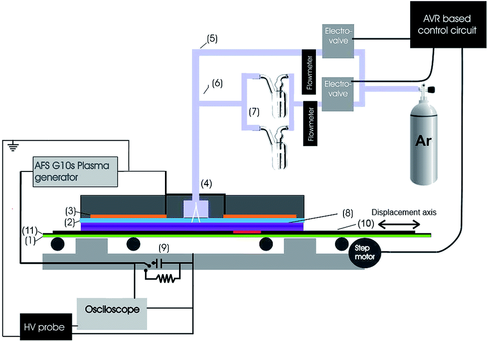 | ||
| Fig. 1 Schematic representation of the plasma DBD reactor. | ||
2.3 Plasma deposition
Prior to each deposition, the plasma reactor was cleaned thoroughly using acetone and ethanol. The deposition started by flushing the reactor with at least 12 slm of Ar for 15 s and igniting the Ar discharge without any precursor. The substrates were initially treated by the argon plasma for one pass, i.e. a full displacement of the bottom electrode from one side of the reactor to the other and then back, in order to clean and activate the substrate. Three passes of plasma deposition were then performed. The speed of the bottom electrode was adjusted so that each point of the substrate would remain in the discharge for 50 s in every pass. The total flow of argon during the deposition was 20 slm and the flow rate was diverted through the bubblers to achieve a certain monomer feed.Knowledge of the exact discharge power was necessary for the accurate calculation of the W/FM parameter. For this reason, the power consumed in the discharge was calculated. It is known from the literature that the energy consumed per discharge cycle (Ep) is equal to the area of the closed loop of the voltage between the two electrodes of the capacitor (Vd) versus the charge crossing the capacitor (Q). The average consumed discharge power (Wc) was then calculated by dividing Ep by the period of the discharge cycle.22–24 A high voltage probe connected between the top electrode and the ground was used to record Vd. The determination of Q was done by measuring the voltage (Vq) between the two plates of the capacitor (Cq = 0.01 μF) connected between the bottom electrode and the ground.
| Q(t) = VqCq | (1) |
The consumed energy per cycle is calculated using the following formula:
 | (2) |
The flow rate was adjusted in order to obtain an equal W/FM for all depositions. The monomer feed (FM) was calculated based on the weight difference of the bubblers before and after each deposition.20 The current was estimated by measuring the voltage drop in a 10 Ω resistor which was connected in series with the plasma reactor (see Fig. 1).
3. Morphological characterization techniques
High resolution electron microscopy images of the deposited coatings were acquired by means of a Scanning Electron Microscope (SEM) JEOL JSM-7000F for the morphological study. Samples were coated with a 2 nm Pt/Pd coating to avoid charge accumulation. Images of ×10![[thin space (1/6-em)]](https://www.rsc.org/images/entities/char_2009.gif) 000 and ×100000 magnification were acquired at an accelerating voltage of 10 kV and a working distance of 10 mm.
000 and ×100000 magnification were acquired at an accelerating voltage of 10 kV and a working distance of 10 mm.
The thicknesses of the coatings were estimated by Spectroscopic Ellipsometry (SE). Measurements were performed with a J. Woollam M-2000 variable angle spectroscopic ellipsometer. The spectra were acquired at an angle of 70° within the range of 245 nm to 998.6 nm. For the interpretation of the ellipsometric data, an optical model, based on the morphology that was observed by SEM, which contained the optical parameters of the various sublayers was used. It consisted of an aluminium substrate,25 an Al2O3 layer,26 a compact Cauchy film in which the presence of voids was not taken into consideration and a Cauchy film mixed with empty space on top. The Al2O3 had a fixed thickness of 10 nm, the Cauchy film was used to model the compact part of the plasma polymer and the mixed film was used to model the surface roughness or porosity. For the latter, a Bruggeman effective medium approximation (EMA) model was used for the Cauchy layer with empty space.27,28 Fig. 2 shows a schematic representation of the optical model. The thickness of the compact and rough layers, and the percentage of empty space in the latter, were fitted by minimizing the Mean Square Error (MSE).
 | ||
| Fig. 2 Schematic representation of the model used in the SE. | ||
Atomic Force Microscopy (AFM) was also used to study the surface morphology of the coatings. An XE-100 apparatus from PARK systems was used in a non-contact mode for recording 5 × 5 μm surface mappings.
4. Chemical characterization techniques
Infrared spectra were recorded with a Nicolet 6700 FTIR spectrometer (Thermo) with a single bounce diamond crystal Attenuated Total Reflectance (ATR) setup. The crystal had a circular surface of 1.5 mm diameter in which the measured area was exposed. All FTIR spectra were acquired with a 4 cm−1 resolution, 64 scans and a 45° incidence. Data analysis was performed using OMNIC (version 8.1).Raman spectra were recorded with a LabRAM HR Evolution (Horiba Scientific) confocal Raman microscope. In all experiments, the 532 nm wavelength of a solid state laser with an incident power of 1 mW was focused through a ×100 objective on the surface of the samples. The scattered light was collected by the same objective into a multichannel air cooled CCD detector (spectral resolution < 1 cm−1).
5. Results and discussion
Fig. 3 shows the V–Q Lissajous curves for six different output powers (Wo) and Table 1 shows the estimated Wc values. The W/FM parameter for all depositions had a value near 17.7 ± 0.8 MJ kg−1. These values are considerably lower when compared to the values estimated in previous depositions of AMA.20,29,30 A difference in the nature of the substrates between the low and the high powers could also be macroscopically observed, as a considerable amount of streamers appeared in discharge powers above 31.7 W, while at lower powers streamers only appeared at the edges of the substrates. At low powers, the V–Q Lissajous curves exhibit a parallelogram shape, while at higher powers their edges are slightly deformed, indicating the presence of some residual charge carriers at all times.31 While a certain power is essential to maintain an atmospheric pressure glow discharge, higher power, and subsequently higher current density, is expected to induce a transition to a filamentary discharge.32,33 Indeed, as confirmed by the current measurements (see Fig. 4), higher discharge powers result in more filamentary discharge. There is an obvious transition to a filamentary mode between 18.4 W and 23.3 W. Therefore, the presence of filaments affects the local current density in the discharge and energy distribution among the excited species. | ||
| Fig. 3 V–Q Lissajous curves for six different powers. | ||
| Wo | Wc | Flow rate | FM | W/FM |
|---|---|---|---|---|
| 10 W | 9.2 W | 1 slm | 30 mg min−1 | 18.4 |
| 20 W | 18.4 W | 2 slm | 60 mg min−1 | 18.4 |
| 30 W | 23.3 W | 3 slm | 84 mg min−1 | 16.6 |
| 40 W | 31.7 W | 4 slm | 100 mg min−1 | 19.0 |
| 60 W | 42.6 W | 6 slm | 140 mg min−1 | 18.3 |
| 80 W | 55.9 W | 8 slm | 200 mg min−1 | 16.8 |
 | ||
| Fig. 4 V (black) and dQ/dt (blue) waveforms for three different powers: 9.2 W, 31.7 W and 55.9 W. | ||
5.1 Morphological study
SEM was used to evaluate the morphology of the deposited coatings. Fig. 5 shows images of the deposited coatings and the substrate for comparison. In all cases, the images show complete coverage of the substrate. In the surface of all coatings, some ‘globular’-like features were present. Those features, which were modelled as a rough layer in SE, are products from polymerization in the volume of the discharge. Plasma-produced radicals originating from the initial monomer are recombined in the volume of the discharge, forming sub-micron particles which are then deposited on the substrate. The formation of such particles has already been mentioned in the deposition of silanes.34–37 At low power and low monomer feeds (9 W), these features are smaller and less dense, while when the power increases (18 W, 31.7 W and 42.6 W) they become denser and larger. At 55.9 W, they are incorporated into the coating. In the high magnification images of Fig. 6, the difference in the size of these particles is more evident. This difference in the surface morphology of the coatings indicates a change in the formation mechanism of the plasma polymers. The increase in the discharge current and the monomer flow are expected to influence the density, the mean free path of the excited species and consequently the type of discharge. This would explain a different growth mechanism, in which polymerization in the volume of the discharge is favored at higher powers relative to interactions at the discharge–substrate interface.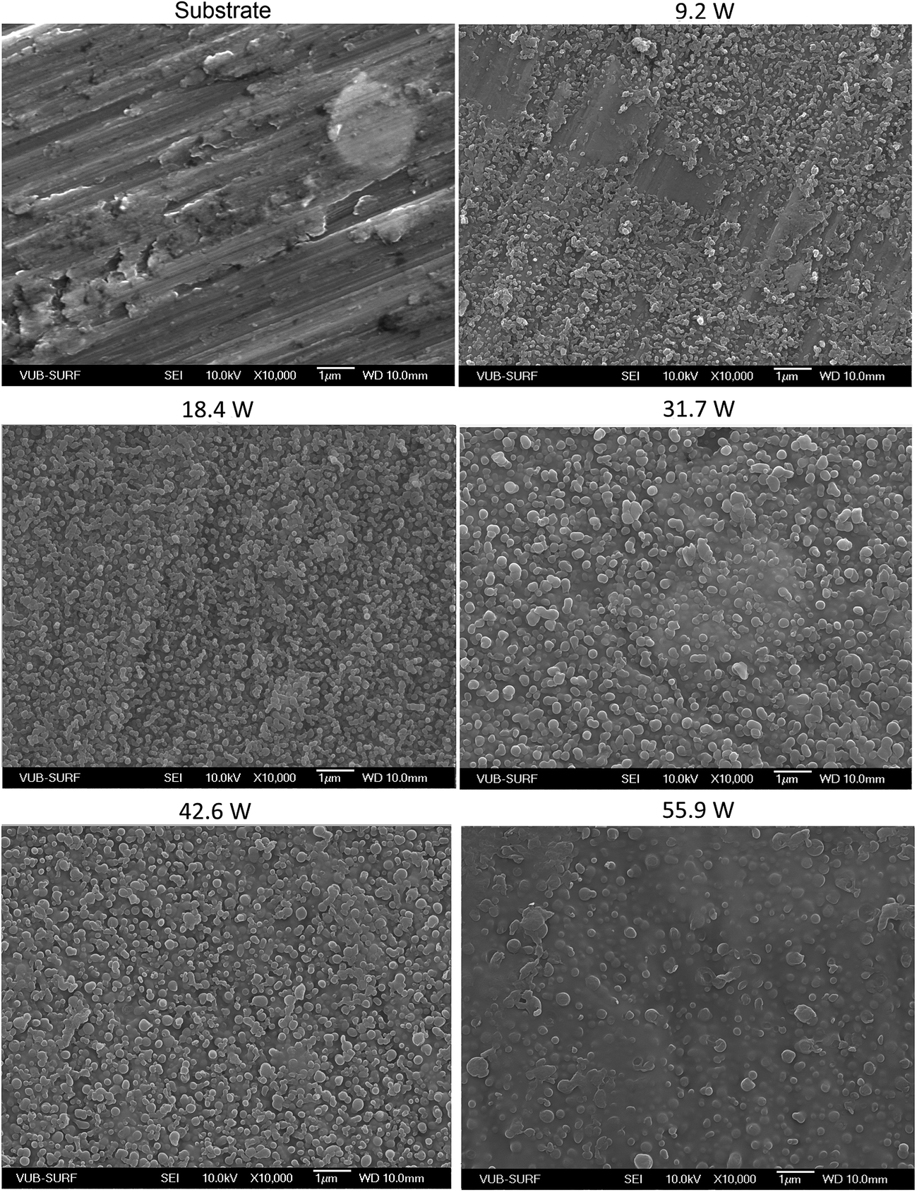 | ||
| Fig. 5 Low magnification (×10000) images of the surface of the deposited coatings. | ||
 | ||
| Fig. 6 High magnification (×100000) images of the surface of the deposited coatings. | ||
The morphology of the coatings was verified by AFM. Fig. 7 shows the topological images of the coatings deposited under different conditions. In agreement with the SEM images, AFM confirms the presence of the features on the surface of the films. Moreover, it confirms the observations of the SEM images concerning the influence of the power/monomer feed on the morphology of the surface. The arithmetic average roughness (Ra) and the ten-point mean roughness (Rz) were also calculated. The Ra was estimated to be near 27 nm for all conditions and the Rz was estimated at 330 nm for coatings deposited with 8 W, lowering to 200 nm for the rest of the deposition.
 | ||
| Fig. 7 AFM images of the surface topology under different deposition conditions. | ||
A model based on the observations of the morphology was used for the SE. Fig. 8 shows the estimated thickness of the compact and rough layers for different deposition parameters. The thickness of the compact layer, and subsequently the deposition rates of the compact layer, increases proportionally with the power. Higher deposition rates can be achieved when both W and F are increased proportionally. The thickness of the rough layer did not substantially vary, with the exception of the 55.9 W film, and was estimated to be between 100 nm and 150 nm. The thickness of this film is in all cases lower than the Rz values calculated by AFM. Since Rz indicates the valley to peak distance it is expected that the thickness of the rough layer should be around this value. The increase in the size of the sub-micron particles, which was observed by SEM, results in a decrease in the empty space in the rough layer. It is practically diminished at 55.9 W, where the sub-micron particles appear to be incorporated into the deposited coating.
 | ||
| Fig. 8 Estimated thickness of the compact and the rough layers and the percentage of voids in the porous film. The W/FM parameter was the same for all depositions. | ||
5.2 Study of the chemistry
The infrared spectra of the deposited coatings are shown in Fig. 9. The plasma polymer bands are broader than those of the conventional polymers, revealing a higher degree of distribution of non-equivalent environments.20 Several absorption bands are common for all the spectra. Among these, the principal ones are the CH2/3 stretching (str) located in the region from 2800 cm−1 to 3000 cm−1, the strong absorption band that appears around 1724 cm−1, which is characteristic for the ester group C![[double bond, length as m-dash]](https://www.rsc.org/images/entities/char_e001.gif) O str, the C–O str that appears near 1150 cm−1 and CH2/3 deformation vibrations at 1460 cm−1 and 1380 cm−1. The very weak peak at 3076 cm−1 observed in the coatings deposited at 23 W, 31.7 W, 42.6 W and 55.9 W is assigned to CH2 str vibrations of the residual CC bonds. This indicates the presence of unreacted allyl groups remaining in the plasma coatings.38–40 The presence of the unreacted allyl groups is confirmed by the presence of the doublet at 984 cm−1 and 934 cm−1, which is attributed to the wagging vibrations of the allyl functionalities. The Al2O3 absorption band also falls in the same region, causing an overlap which makes the distinction of the allyl doublet difficult.41 In the 9.2 W and 18.4 W spectra, the single peak in this region is attributed to Al2O3 since there is no presence of a doublet and the complimentary peak at 3076 cm−1 is missing. In the spectra of the coatings at 23.3 W, 31.7 W and 42.6 W, there is an overlap of the allyl doublet and the Al2O3 band, while in the coating at 55.9 W only the allyl doublet appears. The CC str absorption band near 1645 cm−1, which can barely be observed in the other spectra, confirms the presence of even higher concentrations of unreacted allyl groups.
O str, the C–O str that appears near 1150 cm−1 and CH2/3 deformation vibrations at 1460 cm−1 and 1380 cm−1. The very weak peak at 3076 cm−1 observed in the coatings deposited at 23 W, 31.7 W, 42.6 W and 55.9 W is assigned to CH2 str vibrations of the residual CC bonds. This indicates the presence of unreacted allyl groups remaining in the plasma coatings.38–40 The presence of the unreacted allyl groups is confirmed by the presence of the doublet at 984 cm−1 and 934 cm−1, which is attributed to the wagging vibrations of the allyl functionalities. The Al2O3 absorption band also falls in the same region, causing an overlap which makes the distinction of the allyl doublet difficult.41 In the 9.2 W and 18.4 W spectra, the single peak in this region is attributed to Al2O3 since there is no presence of a doublet and the complimentary peak at 3076 cm−1 is missing. In the spectra of the coatings at 23.3 W, 31.7 W and 42.6 W, there is an overlap of the allyl doublet and the Al2O3 band, while in the coating at 55.9 W only the allyl doublet appears. The CC str absorption band near 1645 cm−1, which can barely be observed in the other spectra, confirms the presence of even higher concentrations of unreacted allyl groups.
 | ||
| Fig. 9 FTIR absorbance spectra of coatings deposited with a discharge power of 9.2 W, 18.4 W, 23.3 W, 31.7 W, 42.6 W and 55.9 W and a monomer feed adjusted to keep the W/FM parameter constant. | ||
A weak band appears near 766 cm−1 in the coatings deposited with 23.3, 31.7 and 42.6 W, and it is much stronger for 55.9 W. This peak is characteristic of poly(methylmethacrylate) (MMA) and it is attributed to the rocking vibrations of the CH2.39 It is visible when long methylene chains are present and disappears in plasma polymers where the structure is more branched.7 Its presence suggests a more linear, and therefore less branched, structure in the coatings deposited with high power and high monomer feed.
A comparison between the CO str and the CH2/3 str bands provides a good indication of the retention of the ester functionality. The peak areas were calculated by estimating the integral of the spectrum from 1665 cm−1 to 1850 cm−1 for the CO and from 2750 cm−1 to 3100 cm−1 for the CH2/3 str, and linearly removing the background. Table 2 shows the ratios of the CO str:CH2/3 str band areas of the absorbance spectra for the deposited plasma coatings of Fig. 9. The values of the CO:CH2/3 ratios are at the same level as those of coatings deposited in a different DBD reactor.20 Apart from the 9.2 W deposition, there is an increase in the CO:CH2/3 ratio, which indicates a better retention of the ester group, when the coatings are deposited at high power and high monomer feed. The chemistry of the surface of the plasma coating is expected to be different with higher amounts of oxygen, due to several processes that take place after the deposition. When the thickness of the coating is relatively low, its overall chemistry is also affected, which could justify the CO:CH2/3 ratio of the 9.2 W deposition. These changes in the concentration of the ester functionalities, even if they are not significant when compared to the ones produced by different W/FM ratios, are still not negligible, indicating a better retention of the ester functionality when higher power and monomer feed are used.
O infrared bands (1665 cm−1 to 1850 cm−1) to CH2/3 bands (2750 cm−1 to 3100 cm−1) of the different Pd–AMA coatings
| Power [W] | 9.2 | 18.4 | 23.3 | 31.7 | 42.6 | 55.9 |
| CO:CH ratio |
0.96 | 0.81 | 0.85 | 0.86 | 0.93 | 1.01 |
The Raman spectra of the deposited coatings are shown in Fig. 10. The observed peaks have similar positions to the infrared spectra, however their intensity changes, as certain vibrations appear stronger in either the infrared or in the Raman spectra.38,39 In the range between 2850 cm−1 to 3000 cm−1, several overlapping bands due to the vibrations of CHx str are observed, while their deformation vibrations appear near 1450 cm−1.39,42 The CO str vibration is less intense in the Raman spectra and is at 1725 cm−1. The CC str is found at 1647 cm−1. For the coating deposited with 9 W, the intensity of this band is relatively low and overlaps with the CO str which makes the separation of the two peaks difficult. When the deposition takes place at higher powers and monomer feeds, the intensity of the peak clearly increases, indicating a higher concentration of unreacted allyl groups in the coating.
 | ||
| Fig. 10 Raman spectra of coatings deposited with discharge powers of 9 W, 18 W, 23 W, 31.7 W, 42.6 W and 55.9 W and the monomer feed adjusted to keep the W/FM parameter constant. | ||
This increase is more clearly seen by comparing the ratio between the CC str and the CHx str bands. The peak areas were calculated by estimating the area of the spectrum from 1530 cm−1 to 1688 cm−1 for the CC str and from 2780 cm−1 to 3150 cm−1 for the CHx str and then linearly removing the background. A partial overlap area with the CO str is not expected to substantially alter the results. The CO str:CH2/3 str ratio increases when higher powers and monomer feeds are used, which confirms the observations of the infrared spectra (see Table 3).
C bands (1530 cm−1 to 1688 cm−1) to CH2/3 bands (2780 cm−1 to 3150 cm−1) of the different Pd–AMA coatings
| Power [W] | 9.2 | 18.4 | 23.3 | 31.7 | 42.6 | 55.9 |
| CC:CH ratio |
0.075 | 0.067 | 0.068 | 0.105 | 0.149 | 0.119 |
6. Conclusions
In this work, it was shown that the use of a constant W/FM parameter in the same plasma reactor could result in the deposition of coatings with different morphologies and chemistries when both the discharge power and monomer feed were varied proportionally. This change in the deposition mechanism is mainly attributed to the transition of the plasma mode from pseudo-glow discharge43 to filamentary, due to the increase of the plasma density. The increase of both the power and monomer flow also results in higher deposition rates, which in this case varied from 0.3 nm s−1 to 5.7 nm s−1.The morphology of the coatings was substantially different when a low power and monomer flow were used, compared to those deposited at very high powers. More specifically, small particles were observed as features on the surface of the coatings. It appears that they interact with the already deposited material and adhere to the coating. Their size increases with the increase in the power and the monomer flow, occupying a greater amount of the surface. With a further increase in both parameters, they fuse into one rigid film.
The study of the chemistry showed a change of concentration of allyl groups in the coatings. Moreover, an increase in the concentration of ester groups was observed at high powers and high monomer flows. This change, while not critical, was unexpected as it was previously shown that AMA retains its ester functionality better than (nPMA) or PiB when the W/FM changes.30,44 Therefore, for the same W/FM values, similar concentrations of CO groups would be expected.
It should be highlighted that when the W/FM parameter is used in atmospheric pressure plasma, it does not take into consideration the type of discharge, which affects the plasma deposition mechanism. The same W/FM parameter can result in films with different morphologies, different thicknesses and slight changes in the chemistry due to the different type of plasma. It is therefore not recommended to use the W/FM parameter for non-homogeneous discharges. It is however, important to mention that W/FM can be used under certain circumstances, for instance when comparing the chemistry for different W or F, when the other parameter is constant, it does not predict the chemistry of the deposited film even with the same experimental setup.
References
- M. A. Lieberman and A. J. Lichtenberg, Principles of plasma discharges and materials processing, Cambridge University Press, 1994 Search PubMed.
- R. Shishoo, Plasma technologies for textiles, CRC Press, 2007 Search PubMed.
- A. Fridman, Plasma chemistry, Cambridge University Press, 2008 Search PubMed.
- R. D'Agostino, P. Favia, C. Oehr and M. R. Wertheimer, Plasma processes and polymers, Wiley Online Library, 2005 Search PubMed.
- D. Merche, N. Vandencasteele and F. Reniers, Thin Solid Films, 2012, 520, 4219–4236 CrossRef CAS PubMed.
- C. Tendero, C. Tixier, P. Tristant, J. Desmaison and P. Leprince, Spectrochim. Acta, Part B, 2006, 61, 2–30 CrossRef PubMed.
- J. Friedrich, Plasma Processes Polym., 2011, 8, 783–802 CrossRef CAS.
- J. Friedrich, R. Mix and G. Kühn, Surf. Coat. Technol., 2005, 200, 565–568 CrossRef CAS PubMed.
- F. S. Denes and S. Manolache, Prog. Polym. Sci., 2004, 29, 815–885 CrossRef CAS PubMed.
- H. Yasuda, J. Polym. Sci., Part D: Macromol. Rev., 1981, 16, 199–293 CrossRef CAS.
- J. D. Whittle, R. D. Short, D. A. Steele, J. W. Bradley, P. M. Bryant, F. Jan, H. Biederman, A. A. Serov, A. Choukurov and A. L. Hook, Plasma Processes Polym., 2013, 10, 767–778 CrossRef CAS.
- H. K. Yasuda, Plasma Processes Polym., 2005, 2, 293–304 CrossRef CAS.
- R. Morent, N. De Geyter, T. Jacobs, S. Van Vlierberghe, P. Dubruel, C. Leys and E. Schacht, Plasma Processes Polym., 2009, 6, S537–S542 CrossRef CAS.
- N. De Geyter, R. Morent, S. Van Vlierberghe, P. Dubruel, C. Leys, L. Gengembre, E. Schacht and E. Payen, Prog. Org. Coat., 2009, 64, 230–237 CrossRef CAS PubMed.
- M. Tatoulian, F. Arefi-Khonsari, L. Tatoulian, J. Amouroux and J. Borra, Chem. Mater., 2006, 18, 5860–5863 CrossRef CAS.
- M. Bashir, J. M. Rees and W. B. Zimmerman, Surf. Coat. Technol., 2013, 234, 82–91 CrossRef CAS PubMed.
- T. C. Tsai and D. Staack, Abstracts IEEE International Conference on Plasma Science, 2010, p. 1 Search PubMed.
- M. Asandulesa, I. Topala, V. Pohoata and N. Dumitrascu, J. Appl. Phys., 2010, 108, 093310 CrossRef PubMed.
- C. Amorosi, T. Fouquet, V. Toniazzo, D. Ruch, L. Averous, V. Ball and M. Michel, React. Funct. Polym., 2012, 72, 341–348 CrossRef CAS PubMed.
- A. Kakaroglou, G. Scheltjens, B. Nisol, I. De Graeve, G. Van Assche, B. Van Mele, R. Willem, M. Biesemans, F. Reniers and H. Terryn, Plasma Processes Polym., 2012, 9, 799–807 CrossRef CAS.
- J. Petersen, R. Bechara, J. Bardon, T. Fouquet, F. Ziarelli, L. Daheron, V. Ball, V. Toniazzo, M. Michel and A. Dinia, et al., Plasma Processes Polym., 2011, 8, 895–903 CrossRef CAS.
- J. Kriegseis, B. Möller, S. Grundmann and C. Tropea, J. Electrost., 2011, 69, 302–312 CrossRef PubMed.
- T. Manley, Trans. Electrochem. Soc., 1943, 84, 83–96 CrossRef PubMed.
- G. Nersisyan and W. Graham, Plasma Sources Sci. Technol., 2004, 13, 582 CrossRef CAS.
- E. D. Palik, Handbook of optical constants of solids, Academic press, 1998, vol. 3 Search PubMed.
- T. Lichtenstein, Handbook of thin film materials, College of Engineering and Applied Science, University of Rochester, 1979 Search PubMed.
- D. Aspnes, Thin Solid Films, 1982, 89, 249–262 CrossRef CAS.
- G. A. Niklasson, C. Granqvist and O. Hunderi, Appl. Opt., 1981, 20, 26–30 CrossRef CAS PubMed.
- B. Nisol, A. Batan, F. Dabeux, A. Kakaroglou, I. De Graeve, G. Van Assche, B. Van Mele, H. Terryn and F. Reniers, Plasma Processes Polym., 2013, 10, 564–571 CrossRef CAS.
- A. Batan, B. Nisol, A. Kakaroglou, I. De Graeve, G. Van Assche, B. Van Mele, H. Terryn and F. Reniers, Plasma Processes Polym., 2013, 10, 857–863 CAS.
- U. Kogelschatz, Plasma Chem. Plasma Process., 2003, 23, 1–46 CrossRef CAS.
- N. Gherardi, G. Gouda, E. Gat, A. Ricard and F. Massines, Plasma Sources Sci. Technol., 2000, 9, 340 CrossRef CAS.
- H. Conrads and M. Schmidt, Plasma Sources Sci. Technol., 2000, 9, 441 CrossRef CAS.
- A. Bouchoule, Phys. World, 1993, 6, 47–51 CAS.
- H. Kersten, G. Thieme, M. Fröhlich, D. Bojic, D. Tung, M. Quaas, H. Wulff and R. Hippler, Pure Appl. Chem., 2005, 77, 415–428 CrossRef CAS.
- C. Hollenstein, Plasma Phys. Controlled Fusion, 2000, 42, R93 CrossRef CAS.
- S. Letts, D. Myers and L. Witt, J. Vac. Sci. Technol., 1981, 19, 739–742 CrossRef CAS.
- D. W. Mayo, F. A. Miller and R. W. Hannah, Course notes on the interpretation of infrared and Raman spectra, John Wiley and Sons, New York, 2004 Search PubMed.
- G. Socrates, Infrared and Raman characteristic group frequencies: tables and charts, John Wiley and Sons, New York, 2001 Search PubMed.
- M. H. Jamróz, M. E. Jamróz, J. E. Rode, E. Bednarek and J. C. Dobrowolski, Vib. Spectrosc., 2009, 50, 231–244 CrossRef PubMed.
- A. J. Maeland, R. Rittenhouse, W. Lahar and P. V. Romano, Thin Solid Films, 1974, 21, 67–72 CrossRef CAS.
- H. Willis, V. Zichy and P. Hendra, Polymer, 1969, 10, 737–746 CrossRef CAS.
- R. Bartnikas, J. Appl. Phys., 1969, 40, 1974–1976 CrossRef CAS PubMed.
- B. Nisol, G. Arnoult, T. Bieber, A. Kakaroglou, I. De Graeve, G. Van Assche, H. Terryn and F. Reniers, Plasma Processes Polym., 2014, 11, 335–344 CrossRef CAS.
| This journal is © The Royal Society of Chemistry 2015 |