
Bipolar resistive switching behavior of CaTiO3 films grown by hydrothermal epitaxy
Fengzhen Lv,
Cunxu Gao*,
Peng Zhang,
Chunhui Dong,
Chao Zhang and
Desheng Xue*
Key Lab for Magnetism and Magnetic Materials of The Ministry of Education, Lanzhou University, 730000 Lanzhou, China. E-mail: gaocunx@lzu.edu.cn; xueds@lzu.edu.cn; Fax: +86-931-8914160; Tel: +86-931-8912237
First published on 29th April 2015
Abstract
Epitaxial CaTiO3 films, with smooth and dense surface, were fabricated by the promising hydrothermal synthesis on the Nb:SrTiO3(001) substrate. The resulting coated substrates was used to prepare Pt/CaTiO3/Nb:SrTiO3 heterostructure devices. The devices present a bipolar resistive switching behavior. Both high and low resistance states have not obvious degradation within ∼3 h and 1000 cycles measurements, which demonstrates the devices possess excellent retention and endurance characteristics. The resistive switching behavior of the devices can be explained by the trap-controlled space charge limited current conduction mechanism. Moreover, the modulation of the Pt/CaTiO3 Schottky-like barrier under an applied electric field is also responsible for the switching behavior, in the carrier injection-trapped/detrapped process.
1 Introduction
Resistance random access memory (RRAM), as a promising candidate to substitute the conventional memory, is a high-performance nonvolatile memory device based on resistive switching effect.1–4 Compared to other conventional memories, RRAM has its own unique advantages, such as high density, high speed, high scalability, low power consumption and nonvolatile. Recently, a variety of materials, including amorphous semiconductors,5 transition metal oxides6–9 and ferromagnetic materials,10 have been verified that possess the resistive switching effect. This switching effect also can be induced by controlling applied electric field in some ferroelectric films. Zhang et al.11 reported that Pt/BaTiO3/Nb:SrTiO3/Pt heterojunctions exhibited the large rectifying characteristic. Ma et al.12 showed the excellent bipolar resistive switching characteristics in TiO2/BaTiO3/TiO2 multilayer with Pt electrodes. However, this resistive switching behavior has not been systematically reported in pure CaTiO3(CTO), which is a typical perovskite ferroelectric material that has a wide range of application prospect as a component of capacitors, microwave dielectric technology and varistor due to its high permittivity.13,14 On the other hand, although the optical and electric properties of the pure CTO and CTO-based films fabricated by vapor deposition,15 excimer laser deposition16 and pulsed laser deposition17 have been reported, the pure CTO thin films grown by the promising hydrothermal method have not been studied.Hydrothermal synthesis is a popular and promising technique that have recently been applied to fabricate various functional films due to its low temperatures, mild reaction conditions, and inexpensive equipment.18–24 In this study, well-crystallized epitaxial CTO films, with smooth and dense surface, are produced by hydrothermal method on Nb:SrTiO3 (NSTO)(001) substrate. The morphology and structure of the CTO epitaxial films are analysed by scanning electron microscopy (SEM), high-resolution X-ray diffractometry (HRXRD) and transmission electron microscopy (TEM) in detail. What is more, the excellent bipolar resistive switching characteristics, including a large number of switching cycles and a long retention time are achieved in the Pt/CTO/NSTO devices. The bipolar resistive switching behavior is principally attributed to trap-controlled space-charge-limited current (SCLC) conduction, which is controlled by oxygen vacancies (OVs) in the films. The modulation of the Pt/CTO Schottky-like barrier under an applied electric field is also responsible for the resistance switching behavior of the devices, in the carrier injection-trapped/detrapped process. These results above show that our research not only provides an opportunity to further explore electric properties of CTO films, but also expands the potential application of hydrothermal ferroelectric films in the nonvolatile RRAM field.
2 Experiment
2.1 Hydrothermal epitaxy of CTO films
Epitaxial CTO films were synthesized under hydrothermal conditions at 200 °C. CaO and TiO2 (0.2 g) were dissolved in a 65 mL solution of 23 vol% KOH in water, and the mix solution was transferred into a Teflon-lined autoclave. This autoclave was heated for 12 h at 200 °C. The samples was removed from the autoclave, cleaned by deionized water, and then dried ready in the air for further measurement.2.2 Characterization
The morphology and surface roughness of the films were assessed by scanning electron microscopy (SEM; Hitachi S-4800, Chiyoda-ku, Tokyo, Japan) and atomic force microscopy (AFM; MFP-3D, Asylum Research, USA). The phase structure of films was investigated by high-resolution X-ray diffractometry (HRXRD; Bede D1, Durham, UK). To assess the microstructure of films, the samples were measured by transmission electron microscopy (TEM; TecnaiTMG2F30, FEI, Hillsboro, OR, USA), through the standard mechanical thinning and ion-milling processes. The valence states of the films were analysed by X-ray photoelectron spectroscopy (XPS; Kratos AXIS UltraDLD, Manchester, UK). The current–voltage characteristics of the films were examined by Keithley 2400 SourceMeter at room temperature in the air.3 Results and discussion
Fig. 1(a) and (b) display the surface and interface morphologies of the CTO films measured by SEM. As shown in Fig. 1(a), the CTO films have crack-free, dense and smooth surface. The SEM images taken on the top of as-grown samples clearly reveal that the films with full uniformity covered the substrate, which size we used for growth is 5 × 5 mm2. The layer with a uniform thickness of ∼350 nm is clearly exhibited in Fig. 1(b). Fig. 1(c) and (d) exhibit the topography images taken on the different areas of 10 × 10 μm2 and 2 × 2 μm2, respectively. As described in them, the films have a flat, dense and uniform surface with root mean square (RMS) roughness of 5–7 nm, which indicates good surface quality and crystallinity of the samples grown at 200 °C, for 12 h. | ||
| Fig. 1 (a) Top-view SEM image of the CTO films. (b) Cross-sectional SEM image taken in an arbitrary portion of the films. The AFM images taken on the different areas of (c) 10 × 10 μm2 and 2 × 2 μm2. | ||
To directly study the epitaxial orientation of the CTO films with respect to the substrate, the CTO/NSTO(001) orientation relationship was assessed by HRXRD. The symmetric HRXRD longitudinal ω–2θ scans taken for the CTO/NSTO samples are shown in Fig. 2(a). Apart from the (001) (l = 1, 2) diffraction peaks corresponding to the NSTO substrate without any reflections originated from second phase, demonstrating that the CTO films are well (00l) oriented along to the substrate. The out of-plane lattice constant of the as-grown films calculated from the (001) peak is 0.3822 nm, which is smaller than the cubic CTO.25 Fig. 2(b) depicts two-dimensional X-ray reciprocal space mapping (RSM) for the CTO films and NSTO substrate. The strongest spot represents the (201) reflection of NSTO substrate and the weak spot on the top is CTO film. This reflection indicates that the CTO films are epitaxially grown on the NSTO substrate.
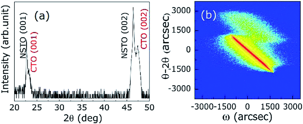 | ||
| Fig. 2 (a) Symmetric HRXRD longitudinal ω–2θ scans of the as-grown CTO films on NSTO(001) substrate. (b) RSM of the films and substrate at around NSTO(201) diffraction. | ||
In order to further confirm this epitaxial growth on NSTO substrate of the CTO hydrothermal films, the TEM measurement was carried out focusing on the interface of the samples. Fig. 3(a) shows a cross-sectional high-resolution transmission electron micrograph of the CTO/NSTO interface along the NSTO[100] zone axis. The lattice planes at the interface between the films and the substrate are clear that directly evident an epitaxial relationship between them, although there might be a few dislocations in the interface to release the internal stress due to slight lattice mismatch. As indicated in the insets [Fig. 3(a)], which are the high-resolution micrographs of the CTO films and NSTO substrate taken in focus, the lattice planes of them are well ordered. Selected area electron diffraction (SAED) patterns of the films and substrate are exhibited in Fig. 3(b) and (c), respectively. Both SAED patterns indicate the highly oriented of the films and epitaxial orientations with small lattice misfit. It is in agreement with the result obtained from HRXRD.
 | ||
| Fig. 3 (a) The cross-sectional high-resolution transmission electron micrograph of the CTO/NSTO(001) interface along the NSTO[100] zone axis. The high-resolution micrographs of the epitaxial CTO films and NSTO substrate taken in focus in the insets, respectively. SAED patterns of (b) CTO films and (c) NSTO substrate, respectively. | ||
Finally, we measured the electron conductivity of the hydrothermal epitaxial CTO films to study the current–voltage (I–V) characteristics in them. Fig. 4 depicts the I–V characteristics of the Pt/CTO/NSTO device under the sweeping voltage of 0 → +2 V → 0 → −2 V → 0, with a voltage step of 0.05 V. A current with compliance of 0.01 A was applied to avoid permanent dielectric breakdown of the device. The numbers and arrows represent the bias voltage sweeping sequences and directions. The inset of Fig. 4 shows that a 200 nm thick Pt layer patterned by the metal mask with a diameter of ∼200 μm was sputtered as electrodes on the CTO film. Al wire was directly connected to NSTO substrate for getting Ohmic contact.24 As shown in Fig. 4, an asymmetric bipolar resistive switching behavior was evidently presented due to the asymmetric Pt/CTO/NSTO structure.
 | ||
| Fig. 4 The I–V characteristic of the Pt/CTO/NSTO device at sweeping voltage of 0 → +2 V → 0 → −2 V → 0. The numbers and arrows represent the voltage sweeping sequences and directions, respectively. The schematic device structure for the measurement is displayed in the inset. | ||
In principle, reliability is an important factor for a device to maintain its functions in application. Therefore, both retention and endurance characteristics of the Pt/CTO/NSTO device have been investigated at room temperature. Fig. 5(a) shows the retention time dependence of the resistance states in the Pt/CTO/NSTO device at the reading voltage of 0.05 V. After applying set voltage of 2 V, the device exhibited the high resistance state (HRS) at 0.05 V and remained HRS even if the voltage was removed. After applying reset voltage of −2 V, the device showed low resistance state (LRS) at 0.05 V and maintained LRS after the voltage was removed. The above steps were executed repeatedly. The HRS and LRS can be easily distinguished. No obvious decay for both HRS and LRS can be found within the measurement time of ∼3 h, which demonstrate that the Pt/CTO/NSTO device possesses a good retention characteristic. Furthermore, electric pulses of +2 V and −2 V (pulse width = 1.2 s) were also alternatively adopted to the device, we examined the resistance at 0.05 V between two neighboring pulses [Fig. 5(b)]. The resistance states can be maintained up to 1000 cycles with a ratio of ∼370 between HRS and LRS, which indicates that the Pt/CTO/NSTO device is fatigue-free within our measured cycles.
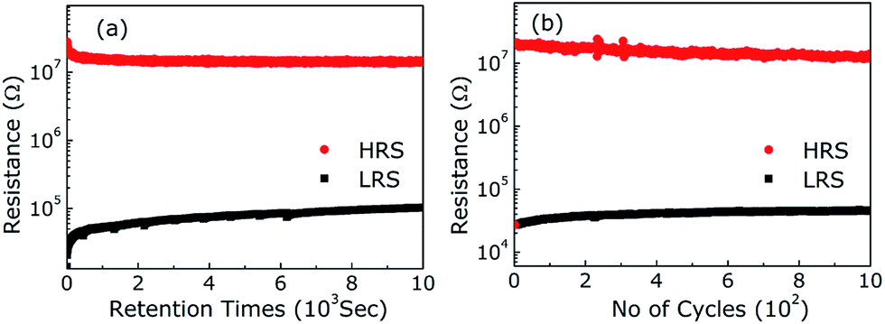 | ||
| Fig. 5 (a) Time up to about 3 h and (b) pulse cycles up to 1000 times for both HRS and LRS measurement in the Pt/CTO/NSTO device at room temperature. | ||
Fig. 6(a) and (b) show the double logarithmic plots of the I–V curve for positive bias and negative bias regions, respectively. The arrows in Fig. 6 represent the voltage sweeping direction. With increasing of positive bias, the current and voltage coincide to a relationship of I ∝ V and I ∝ V2. This relationship of I–V is consistent with the Ohmic law and SCLC conduction.24,26 However, a rapid rise of current, with a slope of ∼5.6. In the backward process, the change between current and voltage follows a slope of ∼2.02 and ∼1.03. The I–V relationship is resemble in the negative bias region [Fig. 6(b)]. In order to further improve application of CTO films for RRAM in the future, deep understanding of switching mechanisms is indispensable.
 | ||
| Fig. 6 The double logarithmic I–V plots for the (a) positive bias region (0–2 V) and (b) negative bias region (−2 V–0 V). | ||
According to recent intensive investigations, many conductive mechanisms have been proposed to interpret the resistive switching behavior in structure of metal–semiconductor/insulator–metal.3,11,12,26–28 Whatever, OVs play an important role in them. We carried out XPS measurement to analyse the condition of OVs in CTO hydrothermal films. Fig. 7 depicts the core-level XPS spectra of Ti and O. As illustrated in Fig. 7(a), the binding energy (Eb) of Ti 2p3/2 and Ti 2p1/2 peaks for the CTO films are 458.47 eV and 464.22 eV, respectively.29,30 The fitting results of the peaks clearly exhibit that the valence state of Ti ions in CTO film is not nominally considered as Ti4+, but Ti3+ and Ti3+ are coexistence. The Ti3+ peaks center at 458.14 eV (2p3/2) and 463.89 eV (2p1/2), Ti4+ peaks positions at 458.58 eV (2p3/2) and 464.42 eV (2p1/2).30 The ratio of these two oxidation states is about 1. The most likely origin of Ti3+ ions in the films is charge compensation of oxygen vacancies (OVs), which are common in perovskite oxides.31 The asymmetric peak of O 1s core-level in Fig. 7(b) demonstrates that amount of OVs (Eb = 531.50 eV), which can be trapping centres and responsible for the bipolar resistive switching behavior, exist in the CTO films.
 | ||
| Fig. 7 XPS spectra of the CTO films, (a) Ti 2p and (b) O 1s photoemission spectra with peak fitting. | ||
As shown in Fig. 6, the resistive switching behavior in the Pt/CTO/NSTO devices can be explained by the Ohmic law and trap-controlled SCLC mechanism.24,26 At low forward voltage, the I–V curve presents linear behavior (I ∝ V), which demonstrates the I–V characteristic obeys Ohmic law, because the density of thermally generated free carriers is predominant over the injected charge carriers in the films. With the voltage increasing, the injected excess charge carriers dominate the thermally generated carriers and are trapped by the shallow traps (OVs) in the films. Thus, current begins to increase so that the resistance decreases and the I–V characteristic obeys SCLC conduction (I ∝ V2). It is noted that the films are the trap-unfilled state in this process. With the forward voltage further increasing, the I–V characteristic is consistent with the transition from the trap-unfilled region to the trap-filled region of SCLC, the current increases sharply with a slope of ∼5.6. Until the voltage increases to the set voltage, the trapping centres are filled by the injected excess carriers. When the applied voltage sweeps back from 2 V to 0, the current still maintains higher value because the trapped carriers are not released from OVs. Subsequently, under negative bias region, the electron concentration in the films still maintains a high level. When the applied voltage drops from reset voltage with a slop of ∼4.77, the trapped carriers begins to be released. It is called as detrapping process. With the voltage further dropping, the electron concentration decreases. And then, while the negative voltage sweeps back close to 0, the electron concentration is lower than the thermally generated carriers, so the relationship between I and V returns to Ohmic law.
Moreover, the modulation of the Schottky-like barrier height and/or width is also responsible to the resistive switching behavior.1,32–34 Under a low negative bias, the resistive state changes from HRS to LRS due to the decrease of the Schottky-like barrier height and/or width at interface. This is induced by the accumulation of OVs, which is controlled by the applied electric field. The I–V curve presents clockwise direction.1 However, applying a large negative voltage, the resistance changes from LRS to HRS. The I–V curve presents an anti-clockwise direction.1 This behavior is corresponded to the I–V characteristic in the Pt/CTO/NSTO devices. Under the positive bias, the height of Pt/CTO Schottky barrier is lowered and the thickness of depletion layer is reduced, because the charge carriers injected from NSTO bottom electrode are trapped by OVs in the depletion layer at Pt/CTO interface. Thus, the resistive state switches from HRS to LRS. Under the negative bias, charge carriers inject from top electrode are obstructed by the Schottky barrier at Pt/CTO interface. This induces a contrary internal electric field across the Schottky barrier and depletion layer. So the trapped carriers are detrapped and emitted from the depletion layer into the bottom electrode. The concentration of charge carriers decrease, the barrier height and/or width and the depletion layer thickness recover to their original states. Thus, the resistance returns from LRS to HRS.
4 Conclusions
To summarize, well-crystallize CaTiO3 films, with high flatness and density, were grown on Nb:SrTiO3(001) substrate at a temperature of 200 °C by hydrothermal epitaxy. The Pt/CaTiO3/Nb:SrTiO3 devices present a bipolar resistive switching behavior. The non-volatile memory characteristics of the devices are investigated at room temperature. No obvious degradation for both high and low resistance states can be found within ∼3 h and ∼1000 cycles measurements, which demonstrates that the Pt/CaTiO3/Nb:SrTiO3 devices possess excellent retention and endurance characteristics. The current conduction analysis reveals that trap-controlled SCLC conduction is principally responsible for the resistive switching behavior of the devices. Furthermore, the modulation of the Pt/CaTiO3 Schottky-like barrier under an applied electric field is also responsible for the resistance switching behavior of the devices, in the carrier injection-trapped/detrapped process. These results above provide an new way to study the properties of hydrothermal epitaxial CaTiO3 films and expand the potential applications of hydrothermal ferroelectric films in the nonvolatile RRAM field.Acknowledgements
This work has been supported to National Basic Research Program of China (no. 2012CB933101), National Natural Science Foundation of China (nos 11274147 and 51371093), PCSIRT (no. IRT1251) and Fundamental Research Funds for the Central Universities (nos lzujbky-2013-ct01, lzujbky-2014-174 and lzujbky-2014-233).References
- K. Shibuya, R. Dittmann, S. Mi and R. Waser, Adv. Mater., 2010, 22, 411–414 CrossRef CAS PubMed.
- R. Waser, R. Dittmann, G. Staikov and K. Szot, Adv. Mater., 2009, 21, 2632–2663 CrossRef CAS PubMed.
- Y. Shuai, X. Ou, W. Luo, A. Mucklich, D. Burger, S. Zhou, C. Wu, Y. Chen, W. Zhang, M. Helm, T. Mikolajick, O. G. Schmidt and H. Schmidt, Sci. Rep., 2013, 3, 2208 Search PubMed.
- R. Waser and M. Aono, Nat. Mater., 2007, 6, 833–840 CrossRef CAS PubMed.
- S. R. Ovshinsky, Phys. Rev. Lett., 1976, 36, 1469 CrossRef CAS.
- M. Janousch, G. I. Meijer, U. Staub, B. Delley, S. F. Karg and B. P. Andreasson, Adv. Mater., 2007, 19, 2232–2235 CrossRef CAS PubMed.
- K. Szot, W. Speier, G. Bihlmayer and R. Waser, Nat. Mater., 2006, 5, 312 CrossRef CAS PubMed.
- J. M. Luo, S. P. Lin, Y. Zheng and B. Wang, Appl. Phys. Lett., 2012, 101, 062902 CrossRef PubMed.
- W. Y. Chang, J. H. Liao, Y. Lo and T. B. Wu, Appl. Phys. Lett., 2009, 94, 172107 CrossRef PubMed.
- W. Hu, L. Zou, R. Chen, W. Xie, X. Chen, N. Qin, S. Li, G. Yang and D. Bao, Appl. Phys. Lett., 2014, 104, 143502 CrossRef PubMed.
- T. J. Zhang, R. K. Pan, Z. J. Ma, M. G. Duan, D. F. Wang and M. He, Appl. Phys. Lett., 2011, 99, 182106 CrossRef PubMed.
- W. J. Ma, S. P. Lin, J. M. Luo, X. Y. Zhang, Y. Wang, Z. X. Li, B. Wang and Y. Zheng, Appl. Phys. Lett., 2013, 103, 262903 CrossRef PubMed.
- G. Pfaff, J. Eur. Ceram. Soc., 1992, 9, 293–299 CrossRef CAS.
- Q. L. Zhang, N. Masó, Y. Liu, H. Yang and A. R. West, J. Mater. Chem., 2011, 21, 12894–12900 RSC.
- E. K. Miiller, B. J. Nicholson and G. Turner, J. Electrochem. Soc., 1963, 110, 969–973 CrossRef PubMed.
- T. Fujii, A. Fujishima, T. Hirano and T. Kobayashi, Appl. Phys. Lett., 1993, 62, 3204 CrossRef CAS PubMed.
- H. Takashima, K. Ueda and M. Itoh, Appl. Phys. Lett., 2006, 89, 261915 CrossRef PubMed.
- F. F. Lange, Science, 1996, 273, 903–909 CAS.
- Y. R. Lin, Y. T. Liu and H. A. Sodano, Appl. Phys. Lett., 2009, 95, 122901 CrossRef PubMed.
- T. Morita and Y. Cho, Appl. Phys. Lett., 2004, 85, 2331 CrossRef CAS PubMed.
- C. Chen, J. R. Cheng, S. W. Yu, L. H. Che and Z. Y. Meng, J. Cryst. Growth, 2006, 291, 135–139 CrossRef CAS PubMed.
- F. Z. Lv, J. Zhang, C. X. Gao, L. Ma, D. Q. Gao, S. M. Zhou and D. S. Xue, Nanoscale Res. Lett., 2014, 9, 266 CrossRef PubMed.
- J. Zhang, Z. L. Yang, F. Z. Lv, C. X. Gao and D. S. Xue, RSC Adv., 2014, 4, 61046 RSC.
- P. Zhang, C. X. Gao, F. Z. Lv, Y. P. Wei, C. H. Dong, C. L. Jia, Q. F. Liu and D. S. Xue, Appl. Phys. Lett., 2014, 105, 152904 CrossRef PubMed.
- K. Parlinski, Y. Kawazoe and Y. Waseda, J. Chem. Phys., 2001, 114, 2395 CrossRef CAS PubMed.
- Y. J. Fu, F. J. Xia, Y. L. Jia, C. J. Jia, J. Y. Li, X. H. Dai, G. S. Fu, B. Y. Zhu and B. T. Liu, Appl. Phys. Lett., 2014, 104, 223505 CrossRef PubMed.
- X. Chen, H. Zhang, K. Ruan and W. Shi, J. Alloys Compd., 2012, 529, 108–112 CrossRef CAS PubMed.
- S. Tsui, A. Baikalov, J. Cmaidalka, Y. Y. Sun, Y. Q. Wang, Y. Y. Xue, C. W. Chu, L. Chen and A. J. Jacobson, Appl. Phys. Lett., 2004, 85, 317 CrossRef CAS PubMed.
- E. R. Vance, R. A. Day, Z. Zhang, B. D. Begg, C. Ball and M. G. Blackford, J. Mater. Sci.: Mater. Med., 1996, 24, 77–82 Search PubMed.
- N. Ohtsu, K. Sato, K. Saito, K. Asami and T. Hanawa, J. Mater. Sci.: Mater. Med., 2007, 18, 1009–1016 CrossRef CAS PubMed.
- J. Wang, J. B. Neaton, H. Zheng, V. Nagarajan, S. B. Ogale, B. Liu, D. Viehland, V. Vaithyanathan, D. G. Schlom, U. V. Waghmare, N. A. Spaldin, K. M. Rabe, M. Wuttig and R. Ramesh, Science, 2003, 299, 1719 CrossRef CAS PubMed.
- F. Miao, J. J. Yang, J. Borghetti, G. M. Ribeiro and R. S. Williams, Nanotechnology, 2011, 22, 254007 CrossRef PubMed.
- C. Wang, K. J. Jin, Z. T. Xu, L. Wang, C. Ge, H. B. Lu, H. Z. Guo, M. He and G. Z. Yang, Appl. Phys. Lett., 2011, 98, 192901 CrossRef PubMed.
- R. Muenstermann, T. Menke, R. Dittmann and R. Waser, Adv. Mater., 2010, 22, 4819–4820 CrossRef CAS PubMed.
| This journal is © The Royal Society of Chemistry 2015 |