
High unipolar strain in samarium-doped potassium–sodium niobate lead-free ceramics
Xiang Lva,
Jiagang Wu*a,
Dingquan Xiaoa,
Yuan Yuana,
Hong Taoa,
Jianguo Zhua,
Xiangjian Wangb and
Xiaojie Loub
aDepartment of Materials Science, Sichuan University, Chengdu 610064, China. E-mail: msewujg@scu.edu.cn; wujiagang0208@163.com
bMulti-disciplinary Materials Research Center, Frontier Institute of Science and Technology, State Key Laboratory for Mechanical Behavior of Materials, Xi'an Jiaotong University, Xi'an 710049, China
First published on 14th April 2015
Abstract
In this work, a high unipolar strain has been developed in the 0.9675(K0.48Na0.52)(Nb0.915Sb0.035Ta0.05)O3–0.0325(Bi1−xSmx)0.5(Na0.82K0.18)0.5ZrO3 (KNNST-B1−xSxNKZ) ceramics by introducing Sm, and the composition dependence of their phase structures and electrical properties is also discussed. The addition of Sm3+ can change the phase structure of the ceramics by simultaneously shifting TR–O and TO–T to a higher temperature, and we obtained a rhombohedral–orthorhombic–tetragonal coexistence phase (R–O–T) with x = 0, a coexistence phase having orthorhombic and tetragonal (O–T) phases with 0.05 ≤ x ≤ 0.60 and an orthorhombic phase with 0.8 ≤ x ≤ 1.0. In addition, the doping with Sm3+ can greatly enhance the unipolar strain of the ceramics without significantly sacrificing its TC, and a high unipolar strain (∼0.28%) was observed in the ceramics with x = 0.20. More importantly, a large Smax/Emax of ∼833 pm V−1 was also observed in the ceramics with x = 0.20 under a low applied electric field of 1.8 kV cm−1. We believe that such a high unipolar strain can benefit the practical applications of actuators.
1. Introduction
Pb(ZrxTi1−x)O3 (PZT) has dominated the market for more than half a century because of its excellent piezoelectricity and is widely being used in sensors, actuators, and transducers.1–7 However, due to the toxic Pb existing in PZT, as well as the rapid increase in environment protection,1–7 considerable efforts have been made to seek an environmentally friendly substitution for PZT.8–28 In particular, after a series of related laws and requirements were published, such as “waste electrical and electronic equipment” (WEEE),6 it is getting more urgent to develop the high-performance lead-free piezoceramics to substitute the lead-based ones.The polymorphic phase boundary (PPB) between orthorhombic (O) and tetragonal (T) phases has been gaining popularity since it was discovered, because it plays an important role in enhancing the piezoelectric properties of ceramics.8–10 The reason why the PPB can enhance the piezoelectric properties is that the ceramics possess a lower energy barrier when the compositions are located at the regions of phase boundaries, greatly facilitating the polarization rotation and extension.8,9 Recently, the electric field-induced strain has been widely studied in the (Bi0.5Na0.5)TiO3-based materials, and then, a giant strain of ∼0.45% was obtained together with a poor d33.11 Unfortunately, although KNN-based ceramics show good piezoelectric properties, a relatively low strain (<0.20%) has always been observed.12–14 Based on the abovementioned viewpoints, we expect to construct the phase boundary by refining the compositions for achieving relatively good piezoelectric properties and a high electrically induced strain.8
Samarium is a rare earth element that has been widely doped into piezoelectric ceramics such as Pb-based,7,15,16 BaTiO3-based,17,18 and Bi0.5Na0.5TiO3 (BNT)-based19,20 ceramics. Sm-substituted (Ba, Pb)(Zr, Ti)O3 ceramics show that Sm3+ can inhibit grain growth, have a “soft” doping effect on piezoelectric properties, and enhance ferroelectric properties, with a reduction in piezoelectric charge coefficient (d33) and coercive field (EC).7 In 2012, M. Raghavender et al. reported that Sm3+ can replace Bi3+ in BNT ceramics, showing an effect on the activation energy for relaxation.20 For the Sm2O3-modified BNT-based ceramics, grain growth was inhibited and the grain became uniform, seriously affecting the electric properties.19 Moreover, a similar result was found in Sm-doped BaTiO3-based ceramics.19 In addition, Sm3+ replacing Bi3+ has also been reported in other material systems such as SrBi8Ti7O27![[thin space (1/6-em)]](https://www.rsc.org/images/entities/char_2009.gif) 21 and SrBi4−xSmxTi3.9Pr0.1O15,22 because Sm3+ and Bi3+ have similar ionic radii and the same valency. As a result, it is reasonable to think that Sm should replace the Bi sites in this material system, and we highly expect to improve the electric properties of KNN-based ceramics by doping Sm in addition to the formation of phase boundaries. In addition, there are few reports on the electric properties of KNN-based ceramics.
21 and SrBi4−xSmxTi3.9Pr0.1O15,22 because Sm3+ and Bi3+ have similar ionic radii and the same valency. As a result, it is reasonable to think that Sm should replace the Bi sites in this material system, and we highly expect to improve the electric properties of KNN-based ceramics by doping Sm in addition to the formation of phase boundaries. In addition, there are few reports on the electric properties of KNN-based ceramics.
In this work, we prepared the 0.9675(K0.48Na0.52)(Nb0.915Sb0.035Ta0.05)O3–0.0325(Bi1−xSmx)0.5(Na0.82K0.18)0.5ZrO3 {abbreviation: KNNST-B1−xSxNKZ 0 ≤ x ≤ 1.0} lead-free ceramics to achieve both a relatively good d33 and a high electric field-induced strain via constructing an orthorhombic–tetragonal coexistence phase. Here, doping with Sm3+ can simultaneously increase TO–T and TR–O with a nearly unchanged TC. As a result, we observed an R–O–T coexistence phase for the ceramics with x = 0, an O–T coexistence phase with 0.05 ≤ x ≤ 0.60, and an O phase with 0.8 ≤ x ≤ 1.0. In particular, a high unipolar strain of ∼0.28% can be attained in the O–T ceramics with x = 0.20, which is superior to the reported results in KNN-based ceramics. The related physical mechanisms were also studied.
2. Experimental procedure
The KNNST-B1−xSxNKZ (x = 0, 0.05, 0.10, 0.20, 0.30, 0.40, 0.50, 0.60, 0.80, 1.0) lead-free piezoceramics were prepared by the conventional mixed oxide method. Raw materials were K2CO3 (99%), Na2CO3 (99.8%), Nb2O5 (99.5%), Ta2O5 (99.99%), Bi2O3 (99.999%), Sb2O3 (99.99%), ZrO2 (99%), and Sm2O3 (99.9%). They were ball milled for 20 h with zirconia ball media and alcohol, after being precisely weighed according to the formula. After calcination at 850 °C for 6 h, the calcined powders were pressed into disks of 9.00 mm diameter and 1 mm thickness under 10 MPa pressure, using PVA as a binder. After burning off the PVA, the pellets were sintered at 1070–1120 °C for 3 h in air. Silver paste was fired on both sides of the samples at 550 °C for 10 min to form the electrodes for the electrical measurements. The samples were poled in a silicon oil bath by applying a direct current electric field of 2–4 kV mm−1 for 30 min at room temperature and phase transition temperatures.X-ray diffraction (XRD) (Bruker D8 Advance XRD, Bruker axs Inc., Madison, WI, Cu-Kα) characterization was done to analyze the phase structures of the ceramics. Field-emission scanning electron microscopy (FE-SEM) (JSM-7500, Japan) was used to measure the surface morphologies of the ceramics. Their piezoelectric constants d33 were tested using a piezo-d33 meter (ZJ-3 A, China), and their planar electromechanical coupling factors kp were measured using an impedance analyzer (HP 4299A). The P–E hysteresis loops were measured at 10 Hz using a radiant precision workstation (USA) with non-poled ceramics. The temperature dependence of the dielectric constant (εr) in each sample was measured using a programmable furnace in connection with an LCR analyzer (HP 4980, Agilent, USA). Finally, strain-electric curves were measured via a precision ferroelectric analyzer (Premier II, Radiant Technologies, Inc., Albuquerque, NM, USA) connected with a miniature plane-mirror interferometer and the accessory laser interferometer vibrometer (SP-S 120/500, SIOS Meβtechnik CmbH, llmenau, Germany).
3. Results and discussion
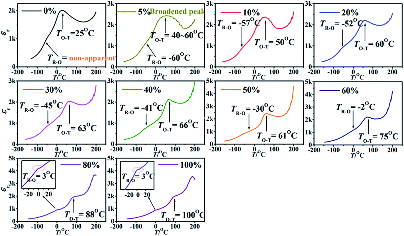
Fig. 1(a) shows the XRD patterns of KNNST-B1−xSxNKZ ceramics using the θ–2θ scan method, measured in the 2θ range of 20–60° and at room temperature. As shown in Fig. 1(a), all samples show a pure perovskite structure, suggesting that Sm3+ can replace Bi3+ without developing a secondary phase. To further analyze the phase revolutions developed by doping with Sm3+, the amplified XRD patterns with 45° ≤ 2θ ≤ 46° are shown in Fig. 1(b). An evident difference in these XRD peaks was observed. In addition, we also simulated the XRD patterns of the ceramics with x = 0, x = 0.20, x = 0.60, and x = 0.80 by the Lorentz method [see Fig. 1(c)], and temperature-dependent dielectric constant curves (εr–T, T = −150 to 200 °C) were also measured [Fig. 2]. As shown in Fig. 2, one can see that both TR–O and TO–T of the ceramics gradually increase with an increase in x, that is, TR–O increases from −60 °C to 3 °C and TO–T increases from 25 °C to 100 °C with x increasing from 0 to 1.0. However, TR–O of the ceramics with x = 0 is non-apparent because of a deeply suppressed dielectric peak. Finally, we defined that the ceramics with x = 0, 0.05 ≤ x ≤ 0.6 and 0.6 < x ≤ 1.0 possess R–O–T, O–T and O phases, respectively. Moreover, the fittings of the ceramics with x = 0, x = 0.20, x = 0.60, and x = 0.80 can further give evidence for our judgments, as shown in Fig. 1(c). In addition, we also found from Fig. 1(c) that the T phase in the O–T coexistence phase slightly increases in the beginning, then sharply decreases with further increase in x, and finally a pure O phase was observed in the ceramics with x = 0.80 and 1.0. | ||
| Fig. 1 XRD patterns of the ceramics as a function of x, measured at (a) 2θ = 20–60° and (b) 2θ = 45–46°. | ||
 | ||
| Fig. 2 εr–T curves of the ceramics with different x values, measured in the range of −150–200 °C. | ||
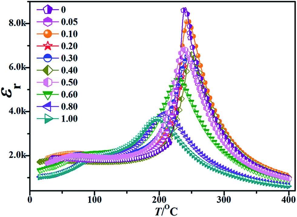
Fig. 3 shows plots of the εr–T curves of the ceramics in the temperature range of 25–450 °C. One can see that the Curie temperature (TC) of the samples firstly increases as x rises from 0 to 0.05, then remains unchanged in the range of 0.05 ≤ x ≤ 0.50, and finally reduces gradually with an increase in x from 0.50 to 1.0. Previously, it was reported that the addition of some ions (such as Sb5+ and Ta5+) into KNN-based ceramics can sharply induce TC.8,23 However, this material system maintains a high TC (∼245 °C) in the region of 0.05 ≤ x ≤ 0.50, suggesting that an appropriate Sm3+ content can stabilize TC or slightly improve TC to a certain extent. Therefore, except for Li+,24 we provide a new way to stabilize TC of the KNN-based ceramics while simultaneously increasing TR–O and TO–T. Based on the data extracted from Fig. 2 and 3, the phase diagram of the ceramics was addressed, as shown in Fig. 4. One can graphically observe from Fig. 4 that the T phase region was getting narrow; however, the R phase region shows an inverse change tendency. In addition, the O phase region is almost unchanged, and TC is slightly decreased. As a result, an O–T coexistence region was seen in the ceramics with 0.05 ≤ x ≤ 0.60, and the O phase was involved in those with 0.6 < x ≤ 1.0.
 | ||
| Fig. 3 εr–T curves of the ceramics as a function of x, measured in the range of 20–400 °C. | ||
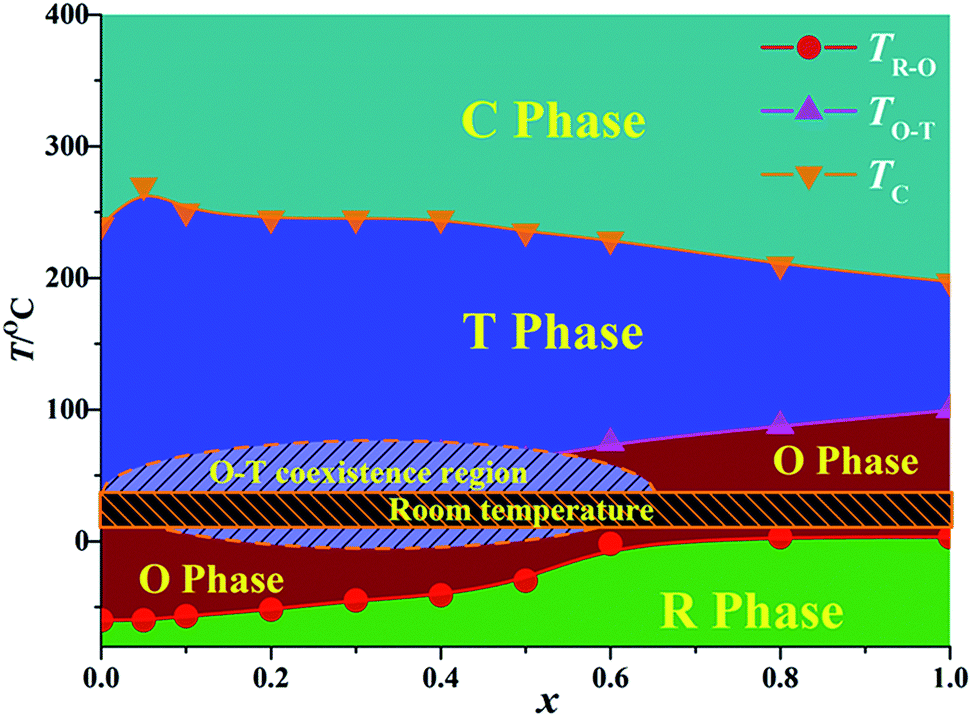 | ||
| Fig. 4 Phase diagram of the ceramics as a function of x. | ||
Fig. 5 plots the variation of dielectric constant (εr) and loss tangent (tanδ) with the compositions and frequencies measured at room temperature (∼20 °C). As shown in Fig. 5, the εr significantly reduces with an increase in x and decreases with increasing frequency, showing a typical characteristic of a normal dielectric or ferroelectric. It is generally accepted that the εr value of KNN-based ceramics is closely related to its grain size, and the εr value decreases with a decreasing grain size.25–28 As shown in Fig. 7 and 8, the average grain size of the ceramics with different x values gradually decreases with an increasing x, which makes an important impact on the declining εr. The declining εr with increasing frequency is due to the different types of polarization mechanisms. At low frequency, εr is determined by three types of polarization mechanisms: electron displacement polarization, ion displacement polarization and turning-direction polarization. However, at high frequency, εr is only determined by electron displacement polarization.18 As for tanδ, a slight change with the compositions was observed, and there is a slight increase with rising frequency.
 | ||
| Fig. 5 εr and tanδ curves of the ceramics as a function of x. | ||
 | ||
| Fig. 6 (a) P–E curves and (b) Pr and Ec values of the ceramics as a function of x. | ||
 | ||
| Fig. 7 FE-SEM patterns and element mappings of the ceramics with different x: (a) x = 0.05, (b) x = 0.20, (c) x = 0.40, and (d) x = 0.60. | ||
 | ||
| Fig. 8 Grain size distribution of the ceramics with (a) x = 0.05, (b) x = 0.20, (c) x = 0.40, and (d) x = 0.60. | ||
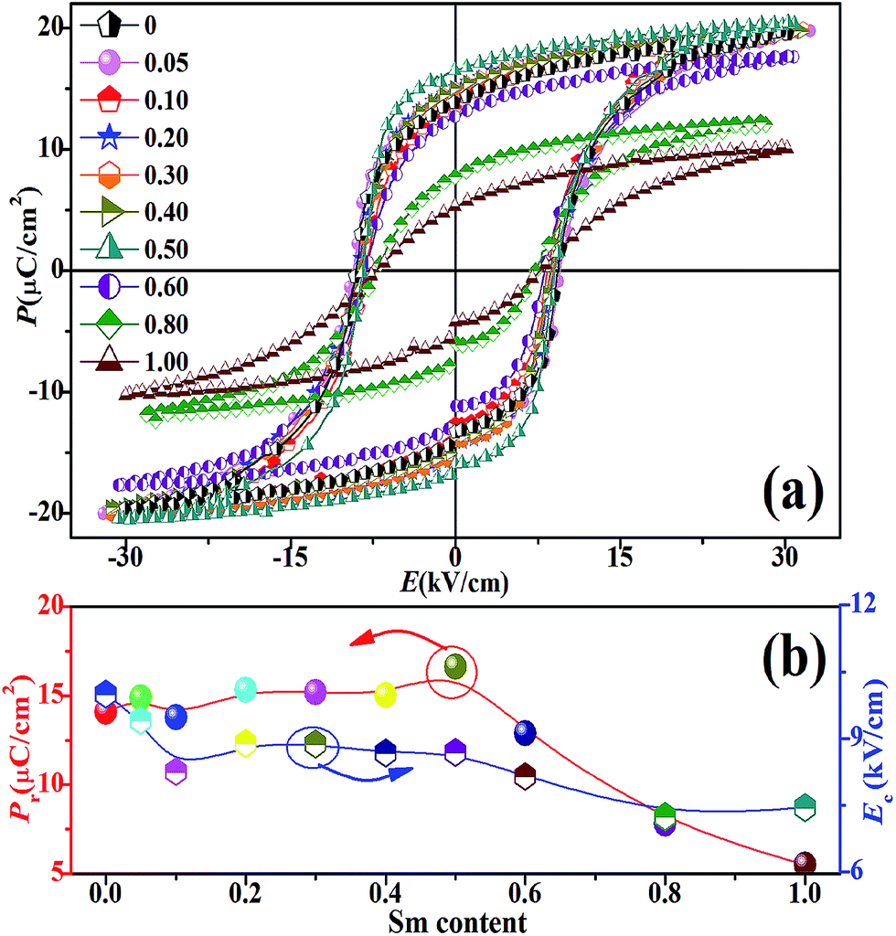
Fig. 6(a) plots the composition dependence of P–E loops of the ceramics measured at f = 10 Hz and room temperature. As shown in Fig. 6(a), there are typical ferroelectric P–E loops, and the saturated ferroelectric P–E loops were observed in the ceramics with 0 ≤ x ≤ 0.60. First, the saturation degree of the P–E loops was improved as x rose from 0 to 0.50 and then was weakened for 0.50 ≤ x ≤ 1.0 because of excess Sm3+, suggesting that the addition of optimum Sm3+ can enhance the ferroelectric properties of the ceramics.7,15,16,18,19,21 Fig. 6(b) gives the composition dependence of Pr & EC values of the ceramics. One can see from Fig. 6(b) that Pr first increases slightly with increasing x from 0 to 0.50 and then decreases significantly when x rises from 0.80 to 1.0. In contrast to Pr, the EC values show a milder change that is, the EC decreases for 0 ≤ x ≤ 0.10, reduces barely for 0.10 ≤ x ≤ 0.50, and decreases gradually as x changes from 0.60 to 1.0.
Generally, the grain sizes of the ceramics play an important role in electrical properties.8,25–28 Here, we characterized the FE-SEM patterns and the corresponding Sm element mappings of the ceramics with x = 0.05, 0.20, 0.40, and 0.60, as shown in Fig. 7(a–d). It can be easily observed that the uniformity of the grain sizes was gradually improved with an increase in x, and Sm element was uniformly distributed into the ceramics. In order to further analyze the grain size evolution, the grain size distributions of the ceramics were measured, as shown in Fig. 8. The ceramics with x = 0.20 possess a relative large grain size and also show a more narrow grain size distribution with respect to the other ones. As shown in the inset of Fig. 8, the average grain sizes of the ceramics slightly increase in the beginning and then significantly reduce as x further increases. A maximum value of average grain size was observed in the KNNST-B0.80S0.20 NKZ ceramics, which is one of the reasons why the ceramics with x = 0.20 have good electrical properties (Smax/Emax),25–28 as will be discussed later.
Fig. 9(a and b) show the plot of the changing tendency of d33 and kp of the ceramics as a function of x, measured at room temperature. All samples were poled at room temperature (∼20 °C). After being poled at room temperature, the d33 firstly reduces slightly as x increases from 0 to 0.05, then increases slightly with an increase of x (0.05 to 0.20), and eventually declines sharply as x further rises up to 1.0. kp shows a similar tendency as d33 except for a sharp increase for x = 0.05–0.20, as shown in Fig. 9(b). Some reasons that may be responsible for this phenomenon are as follows: (i) the change of phase structure. It is well known that the phase structure plays a paramount role in the piezoelectric properties of KNN-based ceramics, where the ceramics with multi-phase coexistence possess lower energy barriers and more polarization vectors than the ones with a single phase.29 In this work, the ceramics with x = 0 possess a R–O–T coexistence phase, which means that the ceramics with x = 0 have more polarization directions and a lower energy barrier than others. Therefore, it is reasonable that the ceramics with x = 0 show more piezoelectric properties than the others. The ceramics with 0.05 ≤ x ≤ 0.60 possess an O–T coexistence phase; the content of the O phase gradually increases as a whole with an increase in x. It is generally accepted that the ceramics with an O phase have a lower d33 with respect to those with a T phase. As a result, d33 decreases as x increases from 0.05 to 0.6 even if the same phase boundary is involved. (ii) The effect of grain sizes. It was reported that the decreased grain sizes can enhance the coupling effect between crystalline grain and grain boundary, which can inhibit the polarization rotation and domain wall motion.25–28 As shown in Fig. 7(a–d) and 8(a and b), the average grain sizes of the ceramics became smaller and smaller as a whole, resulting in a deterioration of piezoelectric properties.
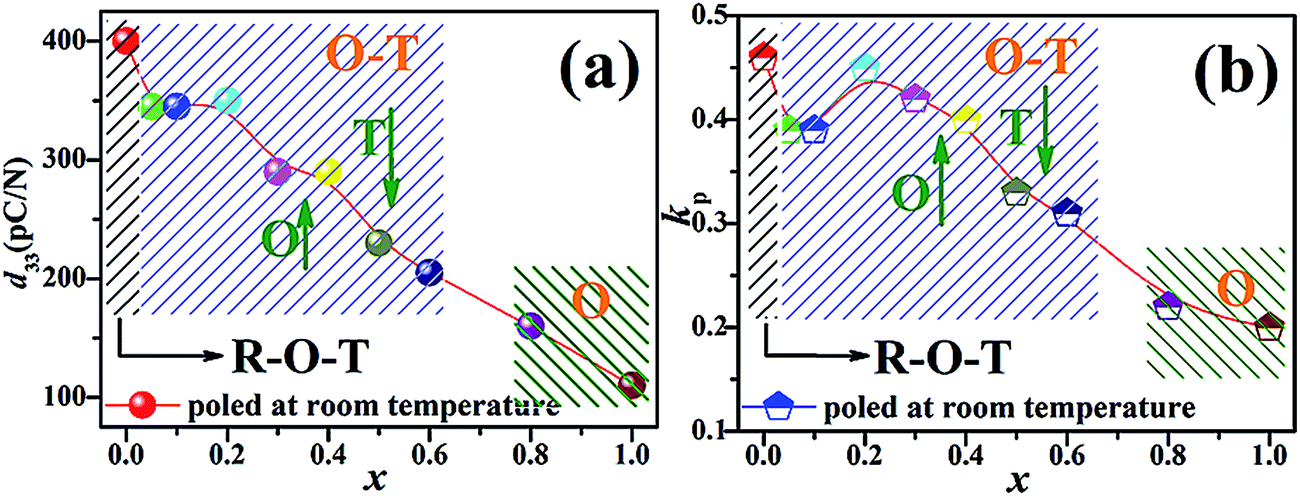 | ||
| Fig. 9 d33 & kp of the ceramics as functions of x. | ||
Fig. 10(a–d) show the unipolar S–E curves, the strain values, the Smax/Emax values, and the relative strain hysteresis (abbreviation: H) of the ceramics with x = 0, 0.05, 0.20, 0.40, 0.60, 0.80, and 1.00. As shown in Fig. 10(a), a slim S–E curve was observed in all the ceramics. We give the maximum strain values of the samples, measured at an approximate electric field of ∼30 kV cm−1 [Fig. 10(b)]. The strain values increase for x = 0–0.20, reach a maximum value (∼0.225%) at x = 0.20, and then significantly reduce with further increase of x (0.20–1.0). As for the Smax/Emax values of the ceramics [see Fig. 10(c)], the Smax/Emax values also reach the maximum value (∼700 pm V−1) at x = 0.20. Fig. 10(d) plots the relative strain hysteresis of the ceramics, and H is calculated by the equation  , where ΔSEmax/2 is the strain difference at the half value of a maximum electric field.30 H gradually increases with increasing x, and the ceramics with x = 0.20 show a relatively low H of 18%. Generally, it is accepted that the Smax/Emax (d*33) values originate from the intrinsic piezoelectric effect and extrinsic domain wall switching.30 However, the applied electric fields play a negligible role in the intrinsic piezoelectric effect, and the d*33 values are mainly dominated by the extrinsic domain wall switching. It is well known that the barrier must be overcome during domain wall switching, and then the multiphase coexistence can greatly facilitate domain wall switching.29 As shown in Fig. 1(a) and 4, the ceramics with x = 0.20 possess an O–T phase coexistence, which can make domain wall switching easier. In addition, the grain size also has an effect on domain wall switching, which means that the moderate and relatively homogeneous grain size can drive domain wall switching easily.29 As shown in Fig. 7(a–d) and 8, the grain sizes of the ceramics with x = 0.20 are moderate and relatively homogeneous than others.
 | ||
| Fig. 10 (a) Unipolar strain curves, (b) the strain values, (c) the Smax/Emax values, and (d) H of the ceramics with x = 0, 0.05, 0.20, 0.40, 0.60, 0.80, and 1.00. | ||
In order to further investigate the electrical properties of the ceramics with x = 0.20, the unipolar strain curves, the strain values, and the d*33 values of the ceramics with x = 0.20 under different driving electric fields were considered and are shown in Fig. 11(a–i), respectively. One can see from Fig. 11(a–g) that the strain values gradually increase with an increase in applied electric fields from 1.8 kV cm−1 to 5.6 kV cm−1, and eventually a maximum strain value of 0.28% was attained under 5.6 kV cm−1. In this work, the unipolar strain value of 0.28% is superior to the reported results in KNN-based ceramics and can almost match that of PZT4 ceramics.31 Of particular interest is the fact that the rising slope of the strain is not unchanged under different levels of applied electric fields, resulting in a demarcation point at 3.0 kV cm−1, as shown in Fig. 11(h). The rising slope of the strain measured before 3.0 kV cm−1 is larger than that measured after 3.0 kV cm−1. Previously, it was reported that both electric field-induced phase transition and domain switching can strongly affect the corresponding strain.23 The strain value is dominated by electric field-induced phase transition under low applied electric fields and dominated by domain switching under high driving electric fields,32 which can explain why there was a demarcation point at 30 kV cm−1, as shown in Fig. 11(h). In addition, the reversibility of the electric field-induced phase transition under low applied electric fields can produce the minimum irreversible strain for a larger useful strain value. Therefore, a large Smax/Emax value of 833 pm V−1 was obtained under a considerably low applied electric field of 1.8 kV cm−1, as shown in Fig. 11(i). However, the domains were partly clamped when the applied electric field was too high, leading to the decrease in Smax/Emax.33
 | ||
| Fig. 11 (a–g) The unipolar strain curves of the ceramics, (h) the strain values, and (i) the Smax/Emax values of the ceramics with x = 0.20 at different driving electric fields. | ||
Fig. 12(a and b) show the d33 and Δd33/d33 against annealing temperatures of the ceramics as a function of Sm3+ content in the range of 0–400 °C. As shown in Fig. 12(a and b), both d33 and Δd33/d33 slightly decline as the annealing temperature increases from room temperature to 200 °C and then significantly decrease with further increase in annealing temperature. The inset of Fig. 12(b) shows the changing tendency of Δd33/d33 as a function of x, measured at the same annealing temperature of 210 °C. As shown in the inset, all Δd33/d33 of the ceramics with x = 0, 0.05, 0.10, 0.20, 0.30, 0.40, and 0.50 show a high value (∼80%), indicating that this material system has a good temperature stability and can be used over a wide temperature range.34
 | ||
| Fig. 12 (a and b) Thermal stability of the ceramics as a function of x, and the inset is the change tendency of Δd33/d33 as a function of x measured at 210 °C. | ||
4. Conclusion
0.9675(K0.48Na0.52)(Nb0.915Sb0.035Ta0.05)O3–0.0325(Bi1−xSmx)0.5(Na0.82K0.18)0.5ZrO3 ceramics were developed by the conventional solid-state reaction method, and a relative good d33 and a high unipolar strain were attained via constructing an orthorhombic–tetragonal phase coexistence. An optimum Sm content can develop a homogeneous and large grain size. A large d33 of 350 pC N−1 and a high strain of 0.28% were simultaneously observed in the ceramics with x = 0.20, and a considerably large Smax/Emax value of 833 pm V−1 was shown in such a ceramic under a low applied electric field of 1.8 kV cm−1 because the reversibility of the electric field-induced phase transition under low applied electric fields can produce the minimum irreversible strain. In addition, the doping with optimum Sm3+ could enhance the ferroelectric properties and lead to good thermal stability, having a negligible effect on TC. Therefore, doping with Sm3+ can promote the unipolar strain of KNN-based ceramics, resulting in promising candidates for actuators.Acknowledgements
We acknowledge the support of the Fundamental Research Funds for the Central Universities (2012SCU04A01), the National Science Foundation of China (NSFC nos 51472169, 51272164, 51332003), the Undergraduate Training Programs for Innovation and Entrepreneurship (201410610178), and the College of Materials Science and Engineering of Sichuan University, and the College of Materials Science and Engineering of Sichuan University. We greatly thank Ms Hui Wang for measuring the SEM patterns.References
- J. F. Tressler, S. Alkoy and R. E. Newnham, Piezoelectric Sensors and Sensor Materials, J. Electroceram., 1998, 2, 257 CrossRef CAS.
- Y. Sugawara, K. Onitsuka, S. Yoshikawa, Q. Xu, R. Newnham and K. Uchino, Metal–Ceramic Composite Actuators, J. Am. Ceram. Soc., 1992, 75, 996 CrossRef CAS PubMed.
- S. Park and T. Shrout, Characteristics of relaxor-based piezoelectric single crystals for ultrasonic transducers, IEEE Trans. Sonics Ultrason., 1997, 44(5), 1140–1147 CrossRef.
- B. Jaffe, R. Roth and S. Marzullo, Piezoelectric Properties of Lead Zirconate–Lead Titanate Solid-Solution Ceramics, J. Appl. Phys., 1954, 25, 809 CrossRef CAS PubMed.
- D. Damjanovic, Ferroelectric, dielectric and piezoelectric properties of ferroelectric thin films and ceramics, Rep. Prog. Phys., 1998, 61, 1267 CrossRef CAS.
- EU-Directive 2002/95/EC, Restriction of the use of certain hazardous substances in electrical and electronic equipment (RoHS), Official Journal of the European Union, L: Legislation, 2003, 46(L37), 19–23 Search PubMed.
- C. Pramila, T. Goel and P. Pillai, Piezoelectric, pyroelectric and dielectric properties of La- and Sm-doped PZT ceramics, J. Mater. Sci. Lett., 1993, 12(21), 1657 CrossRef CAS.
- J. G. Wu, D. Q. Xiao and J. G. Zhu, Potassium–Sodium Niobate Lead-Free Piezoelectric Materials: Past, Present, and Future of Phase Boundaries, Chem. Rev., 2015, 155, 2559–2595 CrossRef PubMed.
- E. Hollenstein, M. Davis, D. Damjanovic and N. Setter, Piezoelectric Properties of Li-and Ta-modified (K0.5Na0.5)NbO3 Ceramics, Appl. Phys. Lett., 2005, 87, 182905 CrossRef PubMed.
- Y. Qin, J. Zhang, Y. Tan, W. Yao, C. Wang and S. Zhang, Domain configuration and piezoelectric properties of (K0.50Na0.50)1−xLix(Nb0.80Ta0.20)O3 ceramics, J. Eur. Ceram. Soc., 2014, 34, 4177 CrossRef CAS PubMed.
- S. Zhang, A. Kounga, E. Aulbach, H. Ehrenberg and J. Rodel, Giant Strain in Lead-Free Piezoceramics Bi0.5Na0.5TiO3–BaTiO3–K0.5Na0.5NbO3 System, Appl. Phys. Lett., 2007, 91(11), 112906 CrossRef PubMed.
- Y. Saito, H. Takao, T. Tani, T. Nonoyama, K. Takatori, T. Homma, T. Nagaya and M. Nakamura, Lead-free Piezoceramics, Nature, 2004, 432, 84 CrossRef CAS PubMed.
- E. Hollenstein, M. Davis, D. Damjanovic and N. Setter, Piezoelectric Properties of Li-and Ta-modified (K0.5Na0.5)NbO3 Ceramics, Appl. Phys. Lett., 2005, 87, 182905 CrossRef PubMed.
- K. Wang, J. Li and J. Zhou, High Normalized Strain Obtained in Li-Modified (K, Na)NbO3 Lead-Free Piezoceramics, Appl. Phys. Express, 2011, 4, 061501 CrossRef.
- B. Jimenez, J. Vicente and R. Jimenez, Extrinsic contributions to the low frequency piezoelectric properties of Ca/Sm modified lead titanate ceramics, J. Phys. Chem. Solid, 1996, 57(4), 389 CrossRef CAS.
- W. Xue, W. Schulze and R. Newnham, Effects of Sm2O3 and Gd2O3 + Nd2O3 on electromechanical properties of PbTiO3 ceramics, J. Am. Ceram. Soc., 1990, 73(6), 1783–1784 CrossRef CAS PubMed.
- H. Sun, X. Wang and X. Yao, Structure and Electric Properties of Sm Doped BaTiO3 Ceramics, Ferroelectrics, 2010, 404(1), 99 CrossRef CAS.
- W. Cai, C. Fu, J. Gao, X. Deng, G. Chen and Z. Lin, Effect of Samarium on the Microstructure, Dielectric and Ferroelectric properties of Barium Titanate Ceramics, Ferroelectrics, 2012, 140(1), 92 CrossRef CAS.
- Y. Zhang, R. Chu, Z. Xu, J. Hao, Q. Chen, F. Peng, W. Li, G. Li and Q. Yin, Piezoelectric and dielectric properties of Sm2O3-doped 0.82Bi0.5Na0.5TiO3–0.18Bi0.5k0.5TiO3 ceramics, J. Alloys Compd., 2010, 502, 341 CrossRef CAS PubMed.
- M. Raghavender, G. Kumar and G. Prasad, Modification of dielectric relaxations in sodium titanate with samarium doping, J. Phys. Chem. Solids, 2006, 67, 8 CrossRef PubMed.
- R. Hou, X. Chen and S. Wu, Substitution of Sm3+ and Nd3+ for Bi3+ in SrBi8Ti7O27 Mixed Aurivillius Phase, Jpn. J. Appl. Phys., Part 1, 2003, 42, 5169 CrossRef CAS.
- S. Padamavathi, J. Omprakash, C. Sameera Devi, M. Vithal, G. Prasad and G. Kumar, Effect of Simultaneous Doping of Pr and Sm on Electrical Conductivity and Relaxation Process in BLSF-SrBi4Ti4O15, Ferroelectrics, 2015, 474(1), 83 CrossRef CAS.
- R. Zuo, J. Fu and D. Lv, Antimony Tuned Rhombohedral–Orthorhombic Phase Transition and Enhanced Piezoelectric Properties in Sodium Potassium Niobate, J. Am. Ceram. Soc., 2010, 93(9), 2783 CrossRef CAS PubMed.
- M. Matsubara, T. Yamaguchi, K. Kikuta and S. Hirano, Effect of Li Substitution on the Piezoelectric Properties of Potassium Sodium Niobate Ceramics, Jpn. J. Appl. Phys., Part 1, 2005, 44, 258 CrossRef CAS.
- K. Kinoshita and A. Yamaji, Grain-size effects on dielectric properties in barium titanate ceramics, J. Appl. Phys., 2008, 47, 371 CrossRef PubMed.
- K. Kakimoto, K. Ando and H. Ohsato, Grain size control of lead-free Li0.06(Na0.5K0.5)0.94NbO3 piezoelectric ceramics by Ba and Ti doping, J. Eur. Ceram. Soc., 2010, 30, 295 CrossRef CAS PubMed.
- S. Tashiro and K. Ishii, Grain Size and Piezoelectric Properties of (Ba, K, Na)NbO3 Lead-Free Ceramics, Jpn. J. Appl. Phys., Part 2, 2006, 114(1329), 386 CAS.
- S. Huo, S. Yuan, Z. Tian, C. Wang and Y. Qiu, Grain Size Effects on the Ferroelectric and Piezoelectric Properties of Na0.5K0.5NbO3 Ceramics Prepared by Pechini Method, J. Am. Ceram. Soc., 2011, 95, 1383 CrossRef PubMed.
- F. Chen, Y. Li, G. Gao, F. Yao, K. Wang, J. Li, X. Li, X. Gao and W. Wu, Intergranular Stress Induced Phase Transition in CaZrO3 Modified KNN-Based Lead-Free Piezoelectrics, J. Am. Ceram. Soc., 2015, 10, 1111 Search PubMed.
- Y. Qin, J. Zhang, Y. Tan, W. Yao, C. Wang and S. Zhang, Domain configuration and piezoelectric properties of (K0.50Na0.50)1−xLix(Nb0.80Ta0.20)O3 ceramics, J. Eur. Ceram. Soc., 2014, 34, 4177 CrossRef CAS PubMed.
- H. Tao, J. Wu, D. Xiao, J. Zhu, X. Wang and X. Lou, High strain in (K, Na)NbO3-Based Lead-Free Piezoceramics, ACS Appl. Mater. Interfaces, 2014, 6, 20358 CAS.
- J. Fu, R. Zuo, H. Qi, C. Zhang, J. Li and L. Li, Low electric-filed driven ultrahigh electrostrains in Sb-substituted (Na, K)NbO3 lead-free ferroelectric ceramics, Appl. Phys. Lett., 2014, 105, 242903 CrossRef PubMed.
- H. Tang, S. Zhang, Y. Feng, F. Li and T. Shrout, Piezoelectric property and stain behavior of Pb(Yb0.5Nb0.5)O3–PbHfO3–PbTiO3 polycrystalline ceramics, J. Am. Ceram. Soc., 2013, 96, 2857 CrossRef CAS PubMed.
- T. Shidmore, T. Comyn and S. Milne, Temperature stability of ([Na0.5K0.5NbO3]0.93–[LiTaO3]0.07) lead-free piezoelectric ceramics, Appl. Phys. Lett., 2009, 94, 222902 CrossRef PubMed.
| This journal is © The Royal Society of Chemistry 2015 |