
Different mechanisms and electrocatalytic activities of Ce ion or CeO2 modified Ti/Sb–SnO2 electrodes fabricated by one-step pulse electro-codeposition†
Tigang Duan,
Ye Chen*,
Qing Wen* and
Ying Duan
Key Laboratory of Superlight Materials and Surface Technology of Ministry of Education, College of Material Science and Chemical Engineering, Harbin Engineering University, Harbin, 15001, Heilongjiang, China. E-mail: chenye@hrbeu.edu.cn; wenqing@hrbeu.edu.cn; Tel: +86-13059004260
First published on 9th February 2015
Abstract
Sb-doped SnO2 electrode was fabricated by the one-step pulse electro-codeposition method, and was modified through either cerium dioxide nanoparticle (nano-CeO2) or cerium ion doping. The results showed that the effects of nano-CeO2 doping and cerium ion doping are quite different. Nano-CeO2 doping shrinks the unit cell volume, improves the degree of crystallinity and refines crystalline grains, while cerium ion doping expands the volume and deteriorates the crystallinity. Nano-CeO2 doping mitigates the surface antimony enrichment and promotes the complete oxidation of antimony so that the majority of antimony oxidation states exist as the Sb5+ state, but cerium ion doping aggravates the enrichment and increases the Sb3+ content. Electrochemical phenol degradation showed that the Ti/Sb–SnO2–CeO2 electrode has a higher degradation efficiency and its kinetic rate constant is 1.46 times as much as that of Ti/Ce–Sb–SnO2. Besides, due to the compact active layer of Ti/Sb–SnO2–CeO2 protecting the titanium substrate from passivation, the accelerated service lifetime of Ti/Sb–SnO2–CeO2 is prolonged, which is 1.28 times as long as that of Ti/Ce–Sb–SnO2.
1. Introduction
Titanium-based anodes, which have also been called dimensionally stable anodes, have been one of the greatest technological breakthroughs of electrochemistry over the last decades, and have promoted the development of electrochemistry.1 Ti-based electrodes have been widely used in various electrochemical fields such as organic electrosynthesis, water electrolysis, the chloro-alkali industry, and electrocatalytic oxidation for organic wastewater treatment.2,3 Among the Ti-based anodes, there are a variety of electrodes such as ruthenium dioxide (RuO2), iridium dioxide (IrO2), lead dioxide (PbO2), manganese oxide (MnO2), tin dioxide (SnO2) and so on.4 Due to the low chlorine evolution overpotential, the RuO2 electrode is suitable for application to chlorine electrolysis.5 IrO2 and MnO2 electrodes are appropriately applied for water electrolysis because of their low oxygen evolution overpotentials.6,7 The antimony-doped tin dioxide (Sb–SnO2) electrode is well known for its low cost, low toxicity, and electro-generation of hydroxyl radicals,8 and is suitable for application to electrocatalytic organic wastewater treatment technology.Although the Sb–SnO2 electrode presents a good catalytic performance, its low service life, which is due to electrode deactivation mainly caused by substrate passivation,9 seriously constrains its practicability. So a great many ideas, such as ion doping, intermediate layer insertion and so on, have been attempted to surmount this shortcoming. The idea of ion doping, including rare earth ion doping,10 noble metal ion doping,11 transition metal ion doing12 and other ion doping,13 has been mostly put into practice through the sol–gel method, the thermal decomposition method and so on. For these methods, however, an amount of repetitive and tedious work has been done inevitably. As for the idea of intermediate layer introduction, TiO2 nanotube array interlayer insertion,14 titanium nitride intermediate layer insertion15 and so on have been attempted. TiO2 nanotube array interlayer insertion and titanium nitride interlayer insertion are novel approaches and can advance the stability significantly without decreasing the activity, but have been only achieved within the lab scale and difficult to reproduce in the practical application.
Recently, for improving the electrode stability, to composite nanomaterials into active coatings by electrodeposition has become a new hot idea and only several related literatures were reported. Hu et al. have reported the impacts of carbon nanotubes and chromium carbides on Sb–SnO2 electrodes.16,17 Zhang et al. have prepared Sb–SnO2 electrode modified with carbon nanotubes and have investigated the performance of electrochemical dye wastewater oxidation.18 In our previous reports, nitrogen-doped graphene nanosheets and titanium nitrides nanoparticles were respectively used to improve the stability and catalytic activity of electrodes.19–21
Herein, cerium dioxide (CeO2) nanoparticles are introduced to modify Sb–SnO2 electrodes. Rare earth elements have been proved to enhance catalytic performance through either acting as a catalyst or assisting catalytic processes,10 thus have been widely studied to modify Sb–SnO2 electrode by means of ion doping. Literatures have reported that the doping of rare earth ions into the active film can improve the surface compactness and enhance the activity for the degradation of organic contaminants.22,23 However, the mechanism about the effects of doping rare earth ions has not been investigated in detail.
In this work, Ti/Sb–SnO2–CeO2 electrode was fabricated by a simple and convenient approach, one-step pulse electro-codeposition, followed by annealing at 600 °C for 2 h. Meanwhile, Ti/Ce–Sb–SnO2 electrode was also prepared for the comparison. To compare the difference between cerium ion doping and nano-CeO2, the morphologies, crystalline structures, surface chemical composition and catalytic activities of electrodes were investigated through scanning electron spectroscopy (SEM), transmission electron spectroscopy (TEM), X-ray diffraction (XRD), X-ray photoelectron spectroscopy (XPS) and electrochemical measurements. During electrodeposition, CeO2 nanoparticles are coated into the depositing layer, refining the depositing grains and improving the layer compactness. After annealing, a compact oxide layer with refined grains is obtained and is favorable to enhancing the electrode stability. In this way, lots of tedious work can also be avoided. And doping nano-CeO2, which acts as catalyst or assisting catalyst, is advantageous to improve the catalytic activity. The modified electrode is expected to achieve enhanced stability and activity.
2. Experimental
2.1. Preparation of electrodes
Prior to the electrodeposition, Ti sheets (0.5 mm thickness, TA0 Type, Japan) were mechanically polished, rinsed with distilled water, and then degreased in a 10% NaOH solution at 85 °C for 1 to 2 h. Afterward, the Ti sheets were etched in 10% oxalic acid at 85 °C for 2 h. Finally, pretreated Ti sheets were preserved in a 3% oxalic acid solution.The electrodeposition solution consisted of 0.1 M SnCl4·5H2O, 0.1 M citric acid and 0.011 M SbCl3. Before electrodeposition, 0.14 g cerium dioxide (CeO2, 20–50 nm, analytical grade; Aladdin Chemicals, Shanghai, China) nanoparticles were mixed into the 100 mL electrodeposition solution and ultrasonically dispersed for 5 min to obtain a homogeneous suspension, and then ethylenediamine tetramethylenephosphonic acid as the additive was added dropwise to the electrolyte to obtain a 1 mM concentration. A graphite rod (spectrum grade, diameter 8 mm; Sinopharm chemical reagent Co. Ltd., Shanghai, China) was employed as the anode, whereas the Ti sheet was used as the cathode. The electrode separation distance was 1 cm. Cathodic square-wave pulse electrodeposition was performed for 0.5 h at an average current density of 5 mA cm−2 and a bath temperature of 23 °C with the pulse conditions of 10 Hz frequency. Ti substrates with deposited layers were then dried at 100 °C and annealed in a muffle furnace at 600 °C for 2 h. Finally, Ti/Sb–SnO2–CeO2 electrodes were obtained. The procedure to prepare Ti/Ce–Sb–SnO2 electrode was the same as mentioned above, except adding 8 mM Ce(NO3)3·5H2O instead of nano-CeO2 (the concentration of Ce ions roughly equals to that of nano-CeO2). And for the preparation of Ti/Sb–SnO2, CeO2 nanoparticles were excluded.
2.2. Characterization of electrodes
The morphologies and crystalline patterns of Ti/Sn–SnO2 and Ti/Sn–SnO2–CeO2 electrodes were examined by scanning electron microscope (SEM, INSPECT S50, America), field emission transmission electron microscope (FETEM, FEI TECNAI G2 F20, America), and X-ray diffractometer (XRD, Cu Kα radiation, 40 kV and 150 mA; Rigaku D/Max2500, Japan). Inductively coupled plasma mass spectroscope (ICP-MS, Xseries II, America) was performed to quantify the amounts of Sn, Sb and Ce dissolution. X-ray photoelectron spectroscope (XPS, Al Kα radiation, hν = 1486.6 eV; Thermo ESCALAB 250, UK) was performed to analyze the composition and chemical state of the surface elements. The spectra were calibrated with respect to the signal of contamination carbon (284.6 eV) as internal reference. The XPS core level spectra were fitted and analyzed using a XPS Peak Processing program with a Lorentzian–Gaussian peak shape after a background subtraction.2.3. Electrochemical experiments
A CHI760C electrochemical workstation (CH Instruments, China) was employed to make electrochemical experiments in a conventional three-electrode system at room temperature. The as-prepared electrode served as the working electrode with a test area of 1 × 1 cm2. A platinum sheet (2 × 2 cm2) and saturated calomel electrode (SCE) were used as a counter and reference electrode, respectively. The supporting electrolyte was 0.25 M Na2SO4 solution. The tests were performed at room temperature. Before each measurement, the system was kept at open circuit potential for 5–10 min until the potential was stable. Cyclic voltammetry (CV) was performed between 0.5 and 1.5 V (vs. SCE) with different sweep rates. The accelerated service life tests were conducted using chronopotentiommetry with an anodic current density of 100 mA cm−2. Electrochemical impedance spectroscopy (EIS) measurements were carried out in a potential of 2.0 V (vs. SCE) with a range of 105 Hz to 0.1 Hz and an amplitude signal of 5 mV, and the results were fitted using the ZView program.The electrochemical phenol degradation experiments were performed in 100 mL 100 mg L−1 phenol solution with the supporting electrolyte of 0.25 M Na2SO4 solution. The electrolysis was performed in the galvanostatic condition of 20 mA cm−2 with an anode area of 1 × 2 cm2 and a Pt cathode area of 2 × 2 cm2. Phenol solution concentrations were examined by UV-Vis spectrophotometer (Agilent UV-Vis 8453, America) using the 4-aminoantipyrine direct spectrophotometric method: 0.5 mL disposed phenol solution was added into 50 mL colorimetric cylinder, 0.5 mL ammonia buffer solution was added and mixed, and 1 mL 4-aminoantipyrine solution (2%) and 1 mL potassium ferricyanide (8%) were added and mixed, and then the colorimetric cylinder was incubated in dark for 10 min, and finally the solution concentration was measured by the absorbance intensity at the characteristic wavelength of 510 nm.
3. Results and discussion
3.1. Characterization of electrodes
The surface morphologies of Ti/Sb–SnO2, Ti/Ce–Sb–SnO2 and Ti/Sb–SnO2–CeO2 electrodes were characterized by SEM shown in Fig. 1. The surface of active oxide layer presents a three-dimensionally microgranular layer for all electrodes. This distinct layer with uniform microparticles can be closely related to the electrode preparation methods. Fig. 1(d) and (e) show uniform distributions of Ce element on the surfaces of active layers. Compared with Ti/Sb–SnO2 and Ti/Ce–Sb–SnO2 electrodes, the CeO2 modified electrode presents a more compact layer with smaller microparticles. On the one hand, smaller particles have larger specific surface area and thus can provide with more catalytic active sites. On the other hand, a compact layer can protect Ti substrate from the exposed oxidization so as to improve the electrode stability. Consequently, Ti/Sb–SnO2–CeO2 electrode can be expected to have improved electrochemical activity and stability. | ||
| Fig. 1 SEM images of (a) Ti/Sb–SnO2, (b) Ti/Ce–Sb–SnO2 and (c) Ti/Sb–SnO2–CeO2 electrodes; (d) and (e) element EDS mapping of Ce distribution for electrodes. | ||
Fig. 2 displays the TEM and HRTEM images of Ti/Ce–Sb–SnO2 and Ti/Sb–SnO2–CeO2 electrodes. Samples for the TEM were scrapped from the titanium substrate, prepared by ultrasonically dispersing the product in ethanol, and then droplets were placed on Cu grids. Fig. 2(a) and (b) show the structure with irregular particles for both electrodes. The HRTEM images of electrodes can provide more information about structure such as crystal lattice. In Fig. 2(c), two uniform interplanar distance values are 0.33 nm and 0.26 nm, which are in agreement with the (110) plane and (101) plane of tetragonal rutile SnO2,24 and other two interplanar distances with values of 0.32 nm and 0.17 nm correspond to the (222) plane and (622) plane of senarmontite Sb2O3 (PDF #43-1071).25 This result shows the active layer of Ti/Ce–Sb–SnO2 electrode has the mixed components of SnO2 and Sb2O3. Fig. 2(d) shows an interplanar distance with the value of 0.19 nm, which is in agreement with the (220) plane of cerianite CeO2 (PDF #43-1002).26 This result shows a successful mixing of nano-CeO2 into the active layer. The corresponding SAED patterns both reflect the polycrystallinity of SnO2 active layers.
 | ||
| Fig. 2 TEM images of (a) Ti/Ce–Sb–SnO2 and (b) Ti/Sb–SnO2–CeO2 electrodes; HRTEM images of (c) Ti/Ce–Sb–SnO2 and (d) Ti/Sb–SnO2–CeO2 electrodes. The insets are the corresponding SAED patterns. | ||
Fig. 3 shows the XRD patterns of Ti substrate, Ti/Sb–SnO2, Ti/Ce–Sb–SnO2 and Ti/Sb–SnO2–CeO2 electrodes. The diffraction peak positions for all electrode samples coincide with those of tetragonal rutile SnO2 (PDF #41-1445) with the diffraction peaks at (110), (101), (200), (211), (220), (310), (112), and (301). The strongest peak is at (110) plane for all samples, suggesting the preferred orientation along the (110) crystallographic direction. The peak intensities of (110), (101), and (211) planes for Ti/Sb–SnO2–CeO2 electrode are stronger than those for Ti/Sb–SnO2 electrode, indicating that the crystallinity of SnO2 for Ti/Sb–SnO2–CeO2 electrode is better and the degree of atomic lattice is higher. However, the intensities of diffraction peaks for Ti/Ce–Sb–SnO2 appear the weakest, revealing the lowest crystallinity; this can be ascribed to the effect of Ce ion doping on the nucleation process and the thermal oxidation process. This result shows that the introduction of CeO2 nanoparticles is favorable to good crystallinity and ordered degree of atomic lattice. No diffraction peaks of antimony oxide and cerium oxide are found from the XRD spectra due to the low doping level (the ICP-MS results show the elemental weight percentage in Table 3). In addition, no peaks for crystallized titanium oxides are observed and only several peaks of metal titanium appear in XRD patterns of all electrodes, suggesting that the Ti substrate is not oxidized in the process of preparation and that the electro-codeposition process can produce a good protection for the Ti substrate.16,17
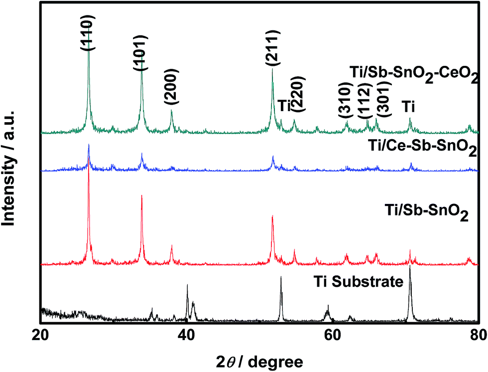 | ||
| Fig. 3 XRD patterns of Ti substrate, and Ti/Sb–SnO2, Ti/Ce–Sb–SnO2 and Ti/Sb–SnO2–CeO2 electrodes. | ||
To further investigate the effects of nano-CeO2 doping and Ce ion doping, the lattice parameter, crystalline size, strain and texture coefficient are discussed in the following, and the analysis results are listed in Table 1.
| Electrode sample | Unit cell parameter | Relative texture coefficient | Crystal size/nm | Strain | ||||
|---|---|---|---|---|---|---|---|---|
| a = b (Å) | c (Å) | V (Å3) | (110) | (101) | (211) | |||
| Ti/Sb–SnO2 | 4.802 | 3.375 | 77.82 | 1.14 | 0.97 | 0.89 | 35.6 | −0.149 |
| Ti/Ce–Sb–SnO2 | 4.835 | 3.372 | 78.82 | 1.06 | 0.93 | 1.01 | 33.2 | −0.141 |
| Ti/Sb–SnO2–CeO2 | 4.805 | 3.378 | 77.99 | 1.00 | 1.00 | 1.00 | 30.8 | −0.150 |
The lattice parameters (a = b and c) for electrodes were calculated by Bragg equation based on the main diffraction peaks of rutile SnO2 phase:
 | (1) |
The crystalline size (D) of the prepared powders was estimated using the Scherrer equation as follows:
 | (2) |
 | (3) |
![[thin space (1/6-em)]](https://www.rsc.org/images/entities/char_2009.gif) cosθ/λ) versus (sinθ/λ).
cosθ/λ) versus (sinθ/λ).
The crystalline sizes of three electrodes determined from the Scherrer equation are 35.6, 33.2, and 30.8 nm, respectively, indicating that CeO2 doping can significantly refine SnO2 crystalline grain. Because of the small crystalline size in nanoscale, lattice strain can be expected from the as-prepared SnO2 layer. The lattice strain can be estimated from the slope of plot of (βcosθ/λ) versus (sinθ/λ). The values for all electrodes are −0.149, −0.141, and −0.150, respectively, indicating the presence of compressive strain in the SnO2 crystal lattice. With the introduction of cerium ions, the compressive strain in SnO2 lattice increases, decreasing the compressive strain. The introduction of nano-CeO2 makes a slight effect on the compressive strain, probably due to the case that cerium ions are not doped into SnO2 lattice. As the doping phase, antimony ions have a smaller ion radius than tin ions and thus may cause the compressive strain in SnO2 host lattice. It can be assumed that the doping of antimony ions with smaller ion radius into the SnO2 host lattice results in the compression of SnO2 lattice but that the doping of cerium ions makes the effect of swelling strain. This assumption is also confirmed by the results.
In addition, the texture coefficient (P(hkl)) is also employed to determine the preferred crystalline orientations. P(hkl) is defined as:28
 | (4) |
In summary, the introduction of nano-CeO2 plays a role in refining crystalline grains and improving the crystallinity, while doping of cerium ions into the SnO2 host lattice improves the preferred orientation along the (211) direction, decreases the compressive strain in the lattice, and increases the unit cell volume. These results can make important effects on the properties of electrodes.
XPS measurements of electrodes were conducted to analyze the chemical states of elements (shown in Fig. 4). Fig. 4(a) shows the XPS survey scan of Ti/Sb–SnO2–CeO2 electrode. Sample has Sn, Sb, Ce, O and C. The presence of C1s results from the organic carbon contamination. Considering the effect of doping CeO2 nanoparticles and doping cerium ions, further investigations were carried out. A comparison of the Sn3d spectra of Ti/Sb–SnO2, Ti/Ce–Sb–SnO2 and Ti/Sb–SnO2–CeO2 electrodes was shown in Fig. 4(b). The spectra reveal the spin–orbit of Sn3d5/2 ground state to be around 486.7 eV while the Sn3d3/2 excited state is observed around 495.1 eV (Table 2), which is ascribed to Sn4+ in SnO2. The gap between the Sn3d5/2 and Sn3d3/2 levels is about 8.4 eV, which closely corresponds to the O in SnO2 and Sn in SnO2, respectively.29 Fig. 4(c) shows the Ce3d spectra of Ti/Ce–Sb–SnO2 and Ti/Sb–SnO2–CeO2 and demonstrates the successful introduction of nano-CeO2 or cerium ions into the deposit layer.
 | ||
| Fig. 4 XPS spectra: (a) survey scanning spectrum, and (b) Sn3d and (c) Ce3d spectra of electrodes; O1s and Sb3d spectra on the surfaces of (d) Ti/Sb–SnO2, (e) Ti/Ce–Sb–SnO2 and (f) Ti/Sb–SnO2–CeO2 electrodes. | ||
| Electrode sample | Binding energy/eV | Atom ratio | ||||||
|---|---|---|---|---|---|---|---|---|
| Sn3d5/2 | Sn3d3/2 | Sb3d3/2 | Oads | Olat | Sn:Sb |
Sb5+:Sb3+ |
Oads:Olat |
|
| Ti/Sb–SnO2 | 486.7 | 495.2 | 540.0 | 531.6 | 530.3 | 6.5 | 1.4 | 0.26 |
| Ti/Ce–Sb–SnO2 | 486.6 | 495.1 | 539.9 | 531.2 | 530.2 | 6.0 | 0.71 | 0.29 |
| Ti/Sb–SnO2–CeO2 | 486.7 | 495.1 | 541.0 | 531.8 | 530.3 | 7.1 | — | 0.35 |
The XPS spectra of Sb3d5/2 and O1s are overlapped, thus they were fitted using XPS Peak Processing Program, the Sb3d5/2 peak is separated from the mixed spectrum (Sb3d5/2 plus O1s), and the results are shown in Fig. 4(d)–(f). Then the O1s peak is split into two peaks and fitted values are given in Table 2. Generally, the O1s peak has been observed at 529–535 eV. And the O1s peak is fitted into two peaks at 530.2–530.3 eV and 531.1–532.9 eV, respectively. The peak at the low binding energy region has been attributed to lattice oxygen species (Olat) which are incorporated into SnO2 crystal lattice, and the peak at the high binding energy region has been ascribed to adsorbed hydroxyl oxygen containing species (Oads) which are adsorbed hydroxyl group.30 For the Sb3d3/2 peak, the intensity for Ti/Sb–SnO2–CeO2 is very slight, which is quite different from that of Ti/Sb–SnO2 and that of Ti/Ce–Sb–SnO2. This situation may be due to the case that the major antimony oxidation states exist as Sb5+ state.31 To investigate the chemical states of antimony element on the electrode surface, the peak of Sb3d3/2 is split into two peaks to character Sb5+ and Sb3+. The peak of Sb3+ appears at the low binding energy region, and the peak of Sb5+ at the high binding energy region.
It is seen from Table 2 that the atom ratio of Sn:Sb is at 6.0–7.1. The doping of cerium ions causes a decrease for the atom ratio of Sn:Sb, showing an increased content of antimony element on the electrode surface. But Ti/Sb–SnO2–CeO2 presents a decreased content of antimony. This phenomenon is probably due to the antimony surface enrichment at high temperature.32 What is possible, antimony and cerium ions competitively doping into the SnO2 host crystalline lattice intensifies the enrichment of antimony on the electrode surface, while the introduction of nano-CeO2 suppresses the antimony enrichment, decreases the surface antimony content and thus benefits to the surface antimony oxidation. Table 3 shows the ICP-MS result and gives the overall weight percentages of individual elements in the as-prepared materials. Observed from the ICP-MS result, the overall atom ratio of Sn and Sb is significantly more than that of XPS result, demonstrating the above analysis. To further investigate the surface antimony states, the Sb3d3/2 peak is split and analyzed, and the atom ratio of Sb5+:Sb3+ is obtained. For the Ti/Sb–SnO2 and Ti/Ce–Sb–SnO2 samples, Sb5+ and Sb3+ coexist on the surface, while Sb5+ as the major antimony oxidation state exists on the surface for Ti/Sb–SnO2–CeO2 sample. Hence the introducing of nano-CeO2 promotes the complete oxidation of antimony in the deposit layer. This result shows that doping cerium ions and doping nano-CeO2 make distinctively different effects on the surface antimony states, which can be expected to have effects on the electrocatalytic activity of as-prepared electrodes for removal of organic contaminants. The atom ratio of Oads:Olat for Ti/Ce–Sb–SnO2 is higher than that of Ti/Sb–SnO2, and it is the highest for Ti/Sb–SnO2–CeO2, implying that the catalytic activity of electrode will be considerably influenced by doping CeO2 nanoparticles.
| Sample | Ce/wt% | Sb/wt% | Sn/wt% | Atom ratio of Sn:Sb |
|---|---|---|---|---|
| Ti/Ce–Sb–SnO2 | 0.51% | 8.22% | 91.28% | 11.4 |
| Ti/Sb–SnO2–CeO2 | 0.62% | 7.89% | 91.49% | 11.9 |
Based on the XRD, XPS and ICP-MS analysis results, a schematic illustration is given out to explain the effects of nano-CeO2 introducing on the electrode surface. In metal oxides, extrinsic aliovalent substitutional doping is widely employed to produce doped conductors for tuning the properties of semiconductor.33 In this approach, the lattice atom is substituted by extrinsic atom with higher or lower valence, introducing shallow electron or hole states into the band structure so as to modify the material performance. In our work, the effects of nano-CeO2 doping and cerium ion doping are investigated. When antimony ions are doped into SnO2 phase, the surface of SnO2 electrode presents the coexistence of Sb5+ and Sb3+ states after annealing at high temperature. With antimony and cerium ions being simultaneously introduced, antimony and cerium are competitively doped into the SnO2 host lattice so as to aggravate the surface antimony enrichment and increases significantly the content of Sb3+. In contrast, the introduction of nano-CeO2 mitigates the surface antimony enrichment and promotes the complete oxidation of antimony so that the major antimony oxidation states exist as Sb5+ state. These indicate that cerium ion doping and nano-CeO2 doping make very different effects. The doping properties of materials can make an important contribution to the oxygen activity, which means influencing the content of adsorbed hydroxyl oxygen containing species on the surface and then determines the electrode activity. Next, the effects on electrocatalytic activity of electrodes will be studied (Scheme 1).
 | ||
| Scheme 1 Schematic representation for the effects of cerium ion doping and nano-CeO2 doping. | ||
3.2. Electrocatalytic performance of electrodes towards phenol
The electrochemical organic degradation experiment have been the most direct and practicable method to investigate the catalytic ability of electrode for the removal of organic contaminants. As shown in Fig. 5, the electrochemical phenol degradation processes were performed on Ti/Sb–SnO2, Ti/Ce–Sb–SnO2 and Ti/Sb–SnO2–CeO2 electrodes, respectively. Observed from Fig. 5(a), the removal efficiencies of phenol increase with electrolysis time. The degradation on Ti/Ce–Sb–SnO2 is more efficient than that on Ti/Sb–SnO2, and Ti/Sb–SnO2–CeO2 is the most efficient among all samples. After 4 h electrolysis, the phenol removal efficiencies are 81.3%, 84.2% and 90.7%, respectively, revealing that the electrocatalytic ability of Ti/Sb–SnO2–CeO2 electrode is the highest. Fig. 5(b) shows the logarithmic relationship of phenol concentration with electrolysis time, and the fitting degrees of curves are above 0.99. Therefore, the phenol degradation process follows the pseudo-first-order kinetics model:| dc/dt = −kc | (5) |
:Olat.
 | ||
| Fig. 5 Electrochemical degradation of phenol (100 mg L−1) on Ti/Sb–SnO2, Ti/Ce–Sb–SnO2, and Ti/Sb–SnO2–CeO2 electrodes with a current density of 20 mA cm−2. (a) Variations of removal efficiency with electrolysis time, and (b) the pseudo-first-order kinetics curves of phenol degradation. The inset is the calibration curve of phenol solution. The supporting electrolyte is 0.25 M Na2SO4 solution. | ||
3.3. Voltammetric characterization
In order to explain the effect of doping nano-CeO2 on the electrocatalytic activity of electrodes, the roughness factor and voltammetric charge of all electrodes were determined from the cyclic voltammetry (CV). Both roughness factor reflecting the real surface area of electrode, and voltammetric charge related to the amounts of electroactive sites, are some of factors to determine electrocatalytic activity.11The roughness factor is defined as real surface area per apparent geometric area of electrode, and calculated through comparing determined capacitance with the capacitance of a smooth oxide surface (8 μF cm−2).34 Fig. 6(a) shows some cyclic voltammograms recorded at different scan rates between 5 and 200 mV s−1 in 0.25 M Na2SO4 solution from 0.7 to 0.8 V (vs. SCE), and only double-layer charging currents were observed. The current densities of Fig. 6(b) were measured in the points of 0.75 V from the CVs for different sweep rates (see Fig. 6(a), S1(a) and (b)).† The linear relationship between current density and sweep rate confirms the nonfaradaic character of current in this potential region.35 The capacitances were obtained from the plot slopes in Fig. 6(b), and they were compared with the value of 8 μF cm−2 to estimate the roughness factor. The results are 42, 90 and 142. Compared with that of Ti/Sb–SnO2, the roughness factor of Ti/Sb–SnO2–CeO2 is boosted (142 versus 42). Thus, the introduction of CeO2 nanoparticles can improve remarkably the roughness of electrode surface and is favorable to the electrocatalytic activity.
 | ||
| Fig. 6 (a) Cyclic voltammgrams between 0.7 and 0.8 V at different sweep rates for Ti/Sb–SnO2–CeO2 in 0.25 M Na2SO4 solution. (b) Evolution of the current density at 0.75 V versus the sweep rate. (c) Reciprocal voltammetric charge (1/q*) versus the square root of the voltammetric scan rate (v1/2). (d) Voltammetric charge (q*) versus the reciprocal square root of the voltammetric scan rate (v−1/2). (c) and (d) data was obtained from the cyclic voltammograms between 0.5 and 1.5 V (vs. SCE) at various scan rates in 0.25 M Na2SO4 solution. | ||
The voltammetric charge (q*) is closely related to the real specific surface area and the amounts of electroactive sites, which greatly determines the electrocatalytic performance of electrode.36 The total voltammetric charge q*T, which is related to the total electrochemically active surface area of the oxide coating, can be obtained through plotting the reciprocal of q* against the square root of the potential scan rate by using the following equation:37
| 1/q* = 1/q*T + kv1/2 | (6) |
The outer voltammetric charge q*O, which is the charge related to the most accessible electroactive surface area, is obtained according to the following equation:
| q* = q*O + k′v−1/2 | (7) |
Fig. 6(c) and (d) show voltammetric charge plots (they are obtained through plotting the voltammetric results in Fig. S1(c)–(e)†) for Ti/Sb–SnO2, Ti/Ce–Sb–SnO2 and Ti/Sb–SnO2–CeO2 electrodes, and linear fittings can be observed. The calculated results of total voltammetric charge are 2.55, 2.64 and 2.75 mC cm−2, respectively, and the results of outer voltammetric charge are 1.08, 1.48 and 1.60 mC cm−2, respectively. These show that the outer voltammetric charge of Ti/Sb–SnO2–CeO2 is 1.48 and 1.08 times as much as that of Ti/Sb–SnO2 and that of Ti/Ce–Sb–SnO2, respectively. This result confirms that Ti/Sb–SnO2–CeO2 electrode possesses the best electrocatalytic activity.
3.4. Electrode stability
Electrodes are investigated through accelerated service life experiments to compare their stabilities. At a high current density, the severe oxygen evolution reaction occurring on the electrode surface aggravates the electrode deactivation. Fig. 7 shows the accelerated service life curves of electrodes. The anode potential is recorded as a function of time, and it indicates that the electrode is deactivated when the potential increases steeply. Ti/Sb–SnO2 electrode displayed a continuous increase by 5 V in potential and got deactivated within 5.3 h. Ti/Ce–Sb–SnO2 demonstrated the similar tendency with Ti/Sb–SnO2–CeO2 in the potential variation with electrolysis time except a small step change from 3.5 V to 3.8 V. And the potential of Ti/Sb–SnO2–CeO2 electrode showed a slow increase with an S-type change. Base on the above situation, the accelerated service life for Sb-doped SnO2 electrodes is defined as the time at which the potential reaches a value of 5.0 V.14 As observed from Fig. 7, the accelerated service lives of Ti/Sb–SnO2 and Ti/Ce–Sb–SnO2 electrodes are 5.3 h and 6.8 h, respectively. And the accelerated life of CeO2 modified electrode is prolonged to 8.7 h, which is 1.28 times as much as that of cerium ion doped electrode. The improved accelerated lifetime can be ascribed to the compact active layer with small crystalline grain size caused by the introduction of CeO2 nanoparticles. The electrode deactivation process will be discussed in the following section. | ||
| Fig. 7 Accelerated service life tests on Ti/Sb–SnO2, Ti/Ce–Sb–SnO2 and Ti/Sb–SnO2–CeO2 electrodes in a 0.25 M Na2SO4 solution with a constant anodic current density of 100 mA cm−2. | ||
3.5. EIS characterization
Herein, EIS experiments were performed with a potential of 2.0 V in 0.25 M Na2SO4 solution. Fig. 8 shows the EIS spectra for Ti/Sb–SnO2, Ti/Ce–Sb–SnO2 and Ti/Sb–SnO2–CeO2 electrodes. In order to depict the electrochemical behaviors of electrodes, the equivalent circuit was used to fit and to model the EIS behavior shown in the inset of Fig. 8(a). The Nyquist plots for all electrodes are similar in form, present two electrochemical processes, and can be characterized by one resistance in the high frequency region, one capacitive-resistive semicircle in the middle frequency region and one depressed capacitive-resistive semicircle in the low frequency region. As shown in Fig. 8(b), the semicircle in the middle frequency region remains constant with potential, while the depressed semicircle in the low gradually shrinks. Considering the electrochemical system in this paper, there are several possible explanations for this situation. | ||
| Fig. 8 (a) Nyquist plots of Ti/Sb–SnO2 and Ti/Sb–SnO2–CeO2 electrodes obtained at 2.0 V, the inset is corresponding equivalent circuit model. (b) Bode plots for Ti/Sb–SnO2–CeO2 electrode at different potentials. | ||
One of possibilities is electrode porosity, meaning that pores and cracks may provide an alternative pathway for faradaic current.38 However, the charge transfer resistances for both processes should decrease with potential, which is not consistent with the observation. Other possibility is the brick model reported by Díaz-Flores et al.39 In a polycrystalline material, a stereo-network of crystal grains separated by the grain boundaries is formed, and grains and grain boundaries are associated different resistivity: the middle frequency semicircle is owed to the grains and the low frequency one with the grain boundaries. However, there is no reasonable statement for the constant resistance of middle frequency semicircle. Additionally, a faradaic reaction along with adsorption and desorption of the reaction intermediates generated through the oxygen evolution reaction process,40 can be also likely to explain the electrochemical processes. In the model, the middle frequency semicircle is rather stable with potential and acts as a constant parallel RC element in series with the oxygen evolution process. Here, the electrochemical processes in our work are well consistent with the adsorption–desorption model.
The resistance in the high frequency corresponds to resistance (R1) in the model and represents the solution resistance caused by the concentration polarization process. The semicircle in the middle frequency corresponds to the capacitance (C2) and resistance (R2) in the model, represents the first electrochemical process. It is supposed to represents the electrochemical behavior of the growth of a resistive hydrated layer at the oxide–solution interface and is rather stable with the potential.40 However, the resistive hydrated layer is not well understood. Among the electrodes for electrochemical wastewater treatment, SnO2 electrode is well known for the electro-generation of hydroxyl radicals. Thus it is a plausible assumption that the first semicircle can be derived from adsorption and desorption of hydroxyl radicals. Observed from Table 4, Ti/Sb–SnO2–CeO2 electrode has a smallest R2 value.
| Electrode | R1/ohm | R2/ohm | CPE2/F | n2 | R3/ohm | CPE3/F | n3 |
|---|---|---|---|---|---|---|---|
| Ti/Sb–SnO2 | 1.42 | 3.71 | 8.03 × 10⁻⁷ | 1.00 | 35.24 | 1.55 × 10⁻³ | 0.88 |
| Ti/Ce–Sb–SnO2 | 2.71 | 3.31 | 2.97 × 10⁻⁷ | 1.00 | 20.03 | 1.15 × 10⁻³ | 0.88 |
| Ti/Sb–SnO2–CeO2 | 1.82 | 1.61 | 1.04 × 10⁻⁶ | 1.00 | 12.52 | 1.21 × 10⁻³ | 0.90 |
| Deactivated Ti/Sb–SnO2 | 13.9 | 1447 | 5.18 × 10⁻⁹ | 0.91 | 723 | 3.81 × 10⁻⁵ | 0.82 |
| Deactivated Ti/Ce–Sb–SnO2 | 4.85 | 313 | 2.18 × 10⁻⁵ | 0.87 | 320 | 2.14 × 10⁻⁵ | 0.60 |
| Deactivated Ti/Sb–SnO2–CeO2 | 2.07 | 4.30 | 9.04 × 10⁻⁷ | 1.00 | 350 | 4.77 × 10⁻⁵ | 0.86 |
The depressed semicircle in the low frequency region, which behaves as the constant phase element (CPE3) and charge transfer resistance (R3) in the equivalent circuit, represents the electrochemical discharge process. It results from the frequency dispersion which is presented by a CPE and possibly caused by different physicochemical phenomena. Pajkossy deemed that the CPE behavior was mainly caused by the local variations of electrode capacitance which was due to atomic scale inhomogeneity, different crystal structures or defects, and surface adsorption.41 Costa et al. deemed that the CPE behavior was induced by electrode surface morphology such as roughness, porosity, nonuniformity.42 And the major factor causing CPE behaviors during the oxygen evolution was the adsorption of reaction intermediates. Analysis of XRD results reveal that doping antimony element leading to SnO2 lattice defects, applying current pulse, and introducing nano-CeO2 bring about cell volume contraction. And as-prepared electrodes present rough surface. These induce the CPE behavior of Sb-doped SnO2 electrodes.
The behavior of second semicircle demonstrates the electrochemical performance of electrodes. A low charge transfer resistance (corresponding to R3) can reflect a good electrochemical activity. The R3 value of Ti/Sb–SnO2–CeO2 electrode is only 12.52 ohm while that for Ti/Ce–Sb–SnO2 electrode is 20.03 ohm (Table 4), showing a prominent improvement of electrochemical performance for electrodes. This result reveals the contribution of nano-CeO2 to the improved electrode activity.
To understand the failure mechanism and the effect of nano-CeO2 doping, we did further EIS for deactivated electrodes. The electrode deactivation can be understood: during the accelerated life test, the intense generation of oxygen bubbles occurs on the electrode surface, and it leads to the consumption of catalytic layer and/or the formation of an insulating TiO2 layer between the Ti substrate and the catalyst layer; the formation of TiO2 layer is the main cause of the electrode deactivation.14,35,43
Fig. 9 shows the EIS spectra of deactivated electrodes. Similarly, the electrode process consists of one concentration polarization process and two electrochemical reaction processes. Deactivated Ti/Sb–SnO2–CeO2 electrode displays the behaviors of hydrated layer and deactivated SnO2 layer, indicating only the loss of electrochemical activity. However, differing from the situation of deactivated Ti/Sb–SnO2–CeO2, the middle frequency semicircles of other deactivated electrodes present depressed, and the charge transfer resistances (R3) significantly increase by more than one order of magnitude, indicating the electrochemical reaction occurring on the mediated oxide layer which results from the substrate oxidation.
 | ||
| Fig. 9 Nyquist plots of (a) deactivated Ti/Sb–SnO2 and Ti/Ce–Sb–SnO2 electrodes, and (b) deactivated Ti/Sb–SnO2–CeO2 electrodes. | ||
The equivalent circuit model in Fig. 8 is still available to depict the electrochemical behavior on the surface of deactivated Ti/Sb–SnO2–CeO2. For the deactivated CeO2-modified electrode, the semicircle in the middle frequency can be explained by the resistive hydrated layer due to its being not significantly changed and independent of the potential. However, for the deactivated Ti/Sb–SnO2 and Ti/Ce–Sb–SnO2, the electrochemical impedance in the middle frequency is not suitable any longer to be explained as the effect of resistive hydrated layer but the electrochemical process on the mediated oxide layer caused by the titanium substrate passivation. The analysis demonstrates that the deactivation of Ti/Sb–SnO2–CeO2 mainly results from the active layer consumption while the deactivation of Ti/Sb–SnO2 and Ti/Ce–Sb–SnO2 is ascribed to the consumption of catalyst layer and the passivation of titanium substrate. Therefore, the introduction of CeO2 nanoparticles into the active layer can effectively protect the substrate from passivation.
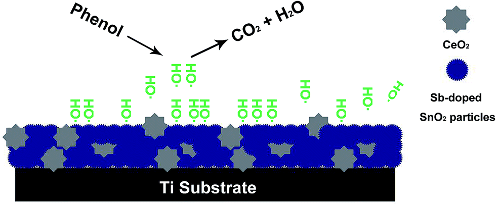
Based on the above analysis results, Scheme 2 is drawn to describe the electrocatalytic phenol degradation process on Ti/Sb–SnO2–CeO2 electrode. On one hand, Ti/Sb–SnO2–CeO2 electrode possesses a high activity to electro-generate hydroxyl radicals as the strong oxidizing species for the degradation of phenol in the aqueous solution. On the other hand, it has a compact SnO2 active layer to protect the substrate from passivation, showing a good stability.
 | ||
| Scheme 2 Schematic representation for the electrocatalytic phenol degradation on Ti/Sb–SnO2–CeO2 electrode. | ||
4. Conclusions
Ti/Sb–SnO2 electrode modified with CeO2 nanoparticles was successfully fabricated by the one-step electro-codeposition method. The influence of CeO2 nanoparticles were investigated through SEM, TEM, XRD, XPS, and electrochemical measurements. Compared with Ti/Sb–SnO2 and Ti/Ce–Sb–SnO2, Ti/Sb–SnO2–CeO2 electrode has smaller crystalline grain size and compact layer which can provide with more active sites. The kinetic analysis of electrochemical phenol degradation shows that the degradation process of phenol coincides with the pseudo-first-order kinetics and that the rate constant on Ti/Sb–SnO2–CeO2 electrode is 0.715 h−1, 1.46 times as much as that on Ti/Sb–SnO2. Voltammetric characterization results show that Ti/Sb–SnO2–CeO2 electrode possesses larger roughness factor and higher specific voltammetric charge for electrocatalytic phenol degradation, explaining the improved electrocatalytic activity of CeO2-modified electrode and the contribution of introducing CeO2 nanoparticles. At last, the deactivation analysis through the impedance spectroscopy indicates that the introduction of nano-CeO2 improves the compactness of active layer to protect electrode from the substrate passivation, and thus enhances the electrode stability. Therefore, the CeO2-modified Ti/Sb–SnO2 electrode presents a high electrocatalytic activity and good stability.Acknowledgements
This work was supported by National Natural Science Foundation of China (no. 51179033 and no. 21476053), the Doctoral Program of the Ministry of Education (no. 20132304110027), the Fundamental Research Funds for the Central Universities (HEUCF201403019), Heilongjiang Postdoctoral Science Research Foundation (LBH-Q12118), and Special Fund Research Program for Talents of Science Technology Innovation in Harbin (no. 2009RFXXG204).References
- S. Trasatti, The electrochemistry of novel materials, ed. J. Lipkowski and P. N. Ross, VCH Publishers, New York, 1994 Search PubMed.
- S. Trasatti, Electrocatalysis: understanding the success of DSA, Electrochim. Acta, 2000, 45, 2377–2385 CrossRef CAS.
- A. N. S. Rao and V. T. Venkatarangaiah, Metal oxide-coated anodes in wastewater treatment, Environ. Sci. Pollut. Res., 2014, 21, 3197–3217 CrossRef PubMed.
- J. Kristóf, E. Horváth and S. Daolio, Study of metal oxide electrocatalytic thin film evolution by thermoanalytical and spectroscopic techniques-a review, Electrocatalysis, 2013, 4, 196–202 CrossRef PubMed.
- V. Trieu, B. Schley, H. Natter, J. Kintrup, A. Bulan and R. Hempelmann, RuO2-based anodes with tailored surface morphology for improved chlorine electro-activity, Electrochim. Acta, 2012, 78, 188–194 CrossRef CAS PubMed.
- W. Hu, S. Chen and Q. Xia, IrO2/Nb-TiO2 electrocatalyst for oxygen evolution reaction in acidic medium, Int. J. Hydrogen Energy, 2014, 39, 6967–6976 CrossRef CAS PubMed.
- M. S. El-Deab, M. I. Awad, A. M. Mohammad and T. Ohsaka, Enhanced water electrolysis: electrocatalytic generation of oxygen gas at manganese oxide nanorods modified electrodes, Electrochem. Commun., 2007, 9, 2082–2087 CrossRef CAS PubMed.
- T. Wu, G. Zhao, Y. Lei and P. Li, Distinctive tin dioxide anode fabricated by pulse electrodeposition: high oxygen evolution potential and efficient electrochemical degradation of fluorobenzene, J. Phys. Chem. C, 2011, 115, 3888 CAS.
- X. Chen, G. Chen and P. L. Yue, Stable Ti/IrOx–Sb2O5–SnO2 anode for O2 evolution with low Ir content, J. Phys. Chem. B, 2001, 105, 4623–4628 CrossRef CAS.
- Y. Cui, Y. Feng and Z. Liu, Influence of rare earths doping on the structure and electro-catalytic performance of Ti/Sb-SnO2 electrodes, Electrochim. Acta, 2009, 54, 4903–4909 CrossRef CAS PubMed.
- R. Berenguer, C. Quijada and E. Morallón, Electrochemical characterization of SnO2 electrodes doped with Ru and Pt, Electrochim. Acta, 2009, 54, 5230–5238 CrossRef CAS PubMed.
- S. Y. Yang, Y. S. Choo, S. Kim, S. K. Lim, J. Lee and H. Park, Boosting the electrocatalytic activities of SnO2 electrodes for remediation of aqueous pollutants by doping with various metals, Appl. Catal., B, 2012, 111–112, 317–325 CrossRef CAS PubMed.
- Y. Wang, T. Brezesinski, M. Antonietti and B. Smarsly, Ordered mesoporous Sb-, Nb-, and Ta-doped SnO2 thin films with adjustable doping levels and high electrical conductivity, ACS Nano, 2009, 3, 1373–1378 CrossRef CAS PubMed.
- Y. Chen, L. Hong, H. Xue, W. Han, L. Wang, X. Sun and J. Li, Preparation and characterization of TiO2–NTs/SnO2–Sb electrodes by electrodeposition, J. Electroanal. Chem., 2010, 648, 119–127 CrossRef CAS PubMed.
- X. Wu, J. Zhang, Y. Wang and A. Huang, Structure and properties of Ti/TiN/Sb-SnO2 electrodes with plasma sprayed TiN interlayer, Adv. Mater. Res., 2013, 602–604, 1613–1616 CAS.
- F. Hu, X. Cui and W. Chen, Pulse Electro-codeposition of Ti/SnO2–Sb2O4–CNT electrode for phenol oxidation, Electrochem. Solid-State Lett., 2010, 13, F20–F23 CrossRef CAS PubMed.
- F. Hu, Z. Dong, X. Cui and W. Chen, Improved SnO2–Sb2O4 based anode modified with Cr3C2 and CNT for phenol oxidation, Electrochim. Acta, 2011, 56, 1576–1580 CrossRef CAS PubMed.
- L. Zhang, L. Xu, J. He and J. Zhang, Preparation of Ti/SnO2–Sb electrodes modified by carbon nanotube for anodic oxidation of dye wastewater and combination with nanofiltration, Electrochim. Acta, 2014, 117, 192–201 CrossRef CAS PubMed.
- T. Duan, Q. Wen, Y. Chen, Y. Zhou and Y. Duan, Enhancing electrocatalytic performance of Sb-doped SnO2 electrode by compositing nitrogen-doped graphene nanosheets, J. Hazard. Mater., 2014, 280, 304–314 CrossRef CAS PubMed.
- T. Duan, Y. Chen, Q. Wen and Y. Duan, Enhanced electrocatalytic activity of nano-TiN composited Ti/Sb–SnO2 electrode fabricated by pulse electrodeposition for methylene blue decolorization, RSC Adv., 2014, 4, 57463–57475 RSC.
- Y. Duan, Q. Wen, Y. Chen, T. Duan and Y. Zhou, Preparation and characterization of TiN-doped Ti/SnO2–Sb electrode by dip coating for orange II decolorization, Appl. Surf. Sci., 2014, 320, 746–755 CrossRef CAS PubMed.
- Y. Feng, Y. Cui, B. Logan and Z. Liu, Performance of Gd-doped Ti-based Sb-SnO2 anodes for electrochemical destruction of phenol, Chemosphere, 2008, 70, 1629–1636 CrossRef CAS PubMed.
- Y. Cui, Y. Feng, J. Liu and N. Ren, Comparison of various organic compounds destruction on rare earths doped Ti/Sb–SnO2 electrodes, J. Hazard. Mater., 2012, 239–240, 225–232 CrossRef CAS PubMed.
- H. G. Yang and H. C. Zeng, Self-Construction of Hollow SnO2 Octahedra Based on Two-Dimensional Aggregation of Nanocrystallites, Angew. Chem., 2004, 116, 6056–6059 CrossRef.
- M. I. Mendivil, B. Krishnan, F. A. Sanchez, S. Martinez, J. A. Aguilar-Martinez, G. A. Castillo, D. I. Garcia-Gutierrez and S. Shaji, Synthesis of silver nanoparticles and antimony oxide nanocrystals by pulsed laser ablation in liquid media, Appl. Phys. A: Mater. Sci. Process., 2013, 110, 809–816 CrossRef CAS.
- A. Vantomme, Z.-Y. Yuan, G. Du and B.-L. Su, Surfactant-Assisted Large-Scale Preparation of Crystalline CeO2 Nanorods, Langmuir, 2005, 21, 1132–1135 CrossRef CAS PubMed.
- F. Gu, S. F. Wang, M. K. Lu, G. J. Zhou, D. Xu and D. R. Yuan, Photoluminescence properties of SnO2 nanoparticles synthesized by sol–gel method, J. Phys. Chem. B, 2004, 108, 8119–8123 CrossRef CAS.
- S. A. Lajevardi and T. Shahrabi, Effects of pulse electrodeposition parameters on the properties of Ni–TiO2 nanocomposite coatings, Appl. Surf. Sci., 2010, 256, 6775–6781 CrossRef CAS PubMed.
- A. R. Babar, S. S. Shinde, A. V. Moholkar, C. H. Bhosale, J. H. Kim and K. Y. Rajpure, Sensing properties of sprayed antimony doped tin oxide thin films: solution molarity, J. Alloys Compd., 2011, 509, 3108–3115 CrossRef CAS PubMed.
- H. He, H. X. Dai and C. T. Au, Defective structure, oxygen mobility, oxygen storage capacity, and redox properties of RE-based (RE = Ce, Pr) solid solutions, Catal. Today, 2004, 90, 245–254 CrossRef CAS PubMed.
- C. Terrier, J. P. Chatelon and J. A. Roger, Analysis of antimony doping in tin oxide thin films obtained by the sol–gel Method, J. Sol-Gel Sci. Technol., 1997, 10, 75–81 CrossRef CAS.
- B. Slater, C. R. A. Catlow, D. H. Gay, D. E. Williams and V. Dusastre, Study of surface segregation of antimony on SnO2 surfaces by computer simulation techniques, J. Phys. Chem. B, 1999, 103, 10644–10650 CrossRef CAS.
- S. D. Lounis, E. L. Runnerstrom, A. Llordés and D. J. Milliron, Defect chemistry and plasmon physics of colloidal metal oxide nanocrystals, J. Phys. Chem. Lett., 2014, 5, 1564–1574 CrossRef CAS.
- N. L. Wu, J. Y. Hwang, P. Y. Liu, C. Y. Han, S. L. Kuo, K. H. Liao, M. H. Lee and S. Y. Wang, Synthesis and Characterization of Sb-Doped SnO2 Xerogel Electrochemical Capacitor, J. Electrochem. Soc., 2001, 148, A550–A553 CrossRef CAS PubMed.
- F. Montilla, E. Morallón, A. De Battisti, S. Barison, S. Daolio and J. L. Vázquez, Preparation and characterization of antimony-doped tin dioxide electrodes. part 1. electrochemical characterization, J. Phys. Chem. B, 2004, 108, 5036–5043 CrossRef CAS.
- L. K. Xu and J. D. Scantlebury, Electrochemical surface characterization of IrO2–Ta2O5 coated titanium electrodes in Na2SO4 solution, J. Electrochem. Soc., 2003, 150, B288–B293 CrossRef CAS PubMed.
- S. Ardizzone, G. Fregonara and S. Trasatti, “Inner” and “outer” active surface of RuO2 electrodes, Electrochim. Acta, 1990, 35, 263–267 CrossRef CAS.
- R. Mohammadi, M. Søgaard, T. Ramos, M. Ghassemi and M. B. Mogensen, Electrochemical impedance modeling of a solid oxide fuel cell anode, Fuel Cells, 2014, 14, 645–659 CrossRef CAS.
- L. L. Díaz-Flores, R. Ramírez-Bon, A. Mendoza-Galván, E. Prokhorov and J. González-Hernández, Impedance spectroscopy studies on SnO2 films prepared by the sol–gel process, J. Phys. Chem. Solids, 2003, 64, 1037–1042 CrossRef.
- A. Ourya, A. Kirchev and Y. Bultel, Oxygen evolution on alpha-lead dioxide electrodes in methanesulfonic acid, Electrochim. Acta, 2012, 63, 28–36 CrossRef PubMed.
- T. Pajkossy, Impedance of rough capacitive electrodes, J. Electroanal. Chem., 1994, 364, 111–125 CrossRef CAS.
- F. R. Costa, D. V. Franco and L. M. D. Silva, Electrochemical impedance spectroscopy study of the oxygen evolution reaction on a gas-evolving anode composed of lead dioxide microfibers, Electrochim. Acta, 2013, 90, 332–343 CrossRef CAS PubMed.
- A. Chen and S. Nigro, Influence of a nanoscale gold thin layer on Ti/SnO2–Sb2O5 electrodes, J. Phys. Chem. B, 2003, 107, 13341–13348 CrossRef CAS.
Footnote |
| † Electronic supplementary information (ESI) available. See DOI: 10.1039/c5ra01876e |
| This journal is © The Royal Society of Chemistry 2015 |