The energy band tailored by Al incorporation in solution-processed IZO TFTs

Yana Gaoa, Jianguo Lub, Jianhua Zhanga and Xifeng Li*a
aKey Laboratory of Advanced Display and System Application, Ministry of Education, Shanghai University, Shanghai 200072, China. E-mail: lixifeng@shu.edu.cn
bKey Laboratory of Silicon Materials, Department of Materials Science and Engineering, Zhejiang University, Hangzhou 310027, China

Received 29th January 2015 , Accepted 17th April 2015

First published on 17th April 2015


Abstract

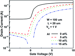
The energy band tailoring of indium zinc oxide (IZO) through Al incorporation was studied and measured directly by ultraviolet photoelectron spectroscopy (UPS). Al doped IZO (AIZO) thin films have lower work function (3.90 eV) and wider bandgap (3.75 eV) compared with IZO (4.15 and 3.5 eV, respectively). These changes induced by Al incorporation would result in higher activation energy and higher flat voltage for AIZO TFTs, which may imply the origin of the AIZO TFTs electrical properties such as threshold voltage shift and off-state current decrease.


Introduction

Amorphous oxide semiconductors (AOSs) are promising candidates as transparent semiconductors for use in the active-matrix backplanes of next-generation displays due to their high carrier mobility, favorable environmental/thermal stability, good optical transparency in the visible region, and potential for low temperature film processing.1–6 However, thin film transistors (TFTs) fabricated with binary oxide semiconductors based on ZnO, In2O3 have some issues such as the instability and high off-state current.2–5 To address the problems, numerous channel materials incorporating a third suppressor element such as ZrInZnO,2,4 HfInZnO,6 AlInZnO7,8 etc. have been investigated since the first use of Ga in 2004.1 Among them, Al was a low cost element and also has a lower standard electrode potential (SEP) (−1.66 V) which makes it more efficiently suppress oxygen-vacancy formation and hence help to achieve a lower off-state current and a large on-to-off current ratio.9 Moreover, Al2O3 has a remarkably larger bandgap (Eg) of ∼9 eV,10 compared to other similar oxide such as ZnO (3.3 eV) and In2O3 (3.6 eV).3 Therefore, it can be expected that the incorporation of Al can control the film electrical characteristics and improve the device performance by controlling the oxygen vacancies and Eg.

Nowadays, most studies on AIZO semiconductors were focused on the fluctuation of oxygen vacancy amount and carrier concentration of those.7,8 However, development of emerging and future applications in the area of thin film transistors with oxide semiconductors requires a detailed control of Fermi level position and a depth study on carrier conduction mechanism.11 In this work, work functions, energy band gap as well as energy band alignment at interfaces influencing carrier conduction are described and discussed. It provides a fundamental understanding of AIZO thin film transistors performance in terms of the energy band tailored by Al incorporation. An intuitional measurement of AIZO work function and valance band energy level was conducted by ultraviolet photoelectron spectroscopy (UPS) along with the UV-visible spectroscopy analysis. The results show that AIZO films have wider energy bandgap and lower work function compared with IZO films. In this paper, we investigated the difference of IZO and AIZO in terms of band bending and carrier conduction mechanism which can explain the reduced off-state current and positive shifted threshold voltage. In addition, chemical solution deposition processes are the most promising for direct deposition, low cost manufacturing, and various compositions of oxide thin films.2,6 Hence, solution processed both oxide semiconductor and gate dielectric TFTs were fabricated in our paper.

Experimental

A 0.3 M AIZO precursor was synthesized by dissolving aluminum chloride (AlCl3), zinc acetate dihydrate (Zn(CH3COO)2·2H2O) and indium nitrate hydrate (In(NO3)3·xH2O) into 2-methoxyethanol (2-MOE). Additionally 0.3 M monoethanolamine (MEA) was added for long-term solution stability. The atomic ratio of In[thin space (1/6-em)]:[thin space (1/6-em)]Zn was fixed at 3[thin space (1/6-em)]:[thin space (1/6-em)]2, and that of Al[thin space (1/6-em)]:[thin space (1/6-em)]In ranged from 0 to 15 at%, (i.e., atomic ratios of Al[thin space (1/6-em)]:[thin space (1/6-em)]In[thin space (1/6-em)]:[thin space (1/6-em)]Zn = 0–0.45[thin space (1/6-em)]:[thin space (1/6-em)]3[thin space (1/6-em)]:[thin space (1/6-em)]2). Considering the fact that AlCl3 is highly reactive and difficult to handle in the ambient, the first step to prepare AIZO solutions was dissolving AlCl3 into 2-MOE in the glovebox with N2 atmosphere. The mixed AIZO solutions were stirred at 400 rpm and 70 °C for 3 hours to form transparent and homogeneous solutions. The solution processed films were spin coated at 3000 rpm. The AIZO films were heated on a hot plate at 150 °C for 15 min and subsequently annealed at 300 °C for 30 min to enable gradual evaporation of the residual solvent. The solution-processed AIZO TFTs with bottom-gate structure were fabricated on a glass substrate. A 100 nm thick ITO film was sputtered on glass substrate as the bottom-gate electrode. Then the aluminum-doped zirconium oxide (AZO) gate dielectric films were deposited by spin-coating.12 A 50 nm thick ITO film as the source and drain electrodes were fabricated also by sputtering. Eventually, the AIZO active layer was subsequently spin-coated on the prepared substrate. The channel width (W) and length (L) ratio of the fabricated TFTs was 5 (L = 20 μm). As we have reported, the relative dielectric constant extracted from a metal–insulator–metal (MIM) capacitor structure was 19.67.12 The Hall mobility, carrier concentration and conductivity were measured by Hall measurement system (HL5500, Bio-Rad). The optical properties were characterized using UV-visible spectrometer (H-3900, Hatachi). The surface properties and compositions of film were examined using an X-ray photoelectron spectroscopy (XPS, Thermo-VG ESCALAB 250) and an UPS. The carbon 1s peak at 284.6 eV was used as a reference for calibration in the XPS results. Grazing incidence X-ray diffraction (XRD, D/MAX-2550) was used to identify phase of the films. The TFTs electrical properties were measured in dark and air using an Agilent 4155C semiconductor parameter analyzer.

Result and discussion

Fig. 1 shows transfer characteristics of solution processed AIZO TFTs annealed at 300 °C as a function of the Al contents from 0 to 15 at%. The measurements were performed by sweeping the gate-to-source voltage (VGS) from −5 to 10 V, with a drain-to-source voltage (VDS) of 1 V. The TFT electrical characteristics are summarized in Table 1. It was obvious that the off-state current decreased from 2.7 × 10⁻⁷ to 1.0 × 10⁻¹¹ A and the threshold voltage (VT) shift to a positive bias region from 0.49 to 1.56 V with the increase of the Al mole ratio. Also the on-off ratio increased from 1.4 × 10³ to 3.0 × 10⁶. When the doping content of Al was 15 at%, however, TFTs exhibited a really low on-state current of 3 × 10⁻⁵ A. It indicated the high Al concentration in the AIZO films lead to a relative low carrier concentration in AIZO films which was accompanied with low on-state and off-state current for these devices.
image file: c5ra01800e-f1.tif
Fig. 1 Transfer (IDSVGS) characteristics of solution processed AIZO TFTs as a function of the Al amounts from 0 to 15 at%. The AIZO TFTs were annealed at 300 °C.
Table 1 Extracted device parameters of AIZO TFTs annealed at 300 °C with the different mole ratio of Al
Al (at%) usat (cm2 V−1 s−1) Ion/off VT (V) S.S (V dec−1)
0 16.99 1.4 × 10³
5 8.03 5.7 × 10⁵ 0.49 0.76
10 6.03 1.0 × 10⁶ 0.89 0.73
15 1.3 3.0 × 10⁶ 1.56 0.51


The saturation mobility (usat) extracted from the transfer curves were listed in Table 1. It can be seen that the addition of Al reduces the saturation mobility which is coincident with the results reported in previous reports.7,8 Furthermore, the subthreshold swing (S.S) was decreased with the increase of Al amounts indicating the decrease of the interface defects densities. This result was mainly originated from surface morphology of AIZO films. Fig. 2 shown the root mean square (RMS) values of IZO and AIZO (10 at%) films annealed at different temperatures. The RMS values of AIZO films were lower than that of IZO films regardless of the annealing temperature. The smooth surface may be original to the amorphous phase of AIZO films.13 XRD results indicated that the AIZO films stay in an amorphous phase at annealing temperatures range from 300 °C to 500 °C. These indicated that the incorporation of Al can attribute to a smoother surface for IZO films which could reduce the defects density and suppress the charge trapping in the interface between the channel and gate dielectric.12 Thus, the S.S was decreased with the increase of Al addition.


image file: c5ra01800e-f2.tif
Fig. 2 RMS values of IZO and AIZO (10 at%) films annealed at different temperatures. Inset is the AFM image of AIZO films annealing at 300 °C.

Overall TFT transfer characteristics were improved and optimized with the Al mole ratio of 10 at%. The results revealed that Al played an important role in suppressing the carrier concentration which was further confirmed by Hall measurement. Because Al atom had a relatively lower SEP than other In and Zn, it was more easily ionized and then strongly combined with oxygen atom, which reduced carrier concentration in the film due to the decrease of the oxygen vacancy serving as a source of carriers.3 The detail effects of Al on the carrier concentration and carrier conduction were analyzed in the following sections, and we focused on the comparison between the AIZO (10 at%) and IZO solutions/films.

To further verify the effects of Al on the electrical properties IZO and AIZO films, Hall measurement was performed. Fig. 3 shows the dependence of carrier concentration and resistivity on the annealing temperature of IZO and AIZO films. For AIZO films annealed at 300 °C, the Hall mobility which calculated through carrier concentration and resistivity decreased from 2.5 to 1.5 cm2 V−1 s−1 as doping of Al. The results were coincided with the changes in mobility of TFTs as shown in Table 1.


image file: c5ra01800e-f3.tif
Fig. 3 Carrier concentration and resistivity of the IZO and AIZO films with varying temperatures (300, 400 and 500 °C).

Moreover, the decreasing carrier concentration resulted in the increasing resistivity. Considering the results of Hall measurement, Al can suppress carrier concentration due to its low SEP (−1.66 V). The higher chemical bonding energy of Al with oxygen, rather than In or Zn, rarely provides oxygen vacancies and therefore lowers the carrier concentration.14 Thus, Al is an effective suppressor of oxygen deficiencies generation originating from the shallow donor level in the sub gap density of states of the amorphous oxide thin film. Consequently, AIZO thin films can be used as active layer due to the decrease in shallow donor level and lowering Fermi level, which were further confirmed in the following sections. Furthermore, as the annealing temperature increased (from 300 °C to 500 °C), the carrier concentration increased and resistivity decreased. A quite similar temperature dependence of electrical behavior of other oxide semiconductors was observed.15

XPS measurements were performed to better understand the chemical and structural differences among AIZO and IZO films. Fig. 4a and (b) shows the XPS spectra of In and Zn ions for IZO and AIZO films annealed at 300 °C. Compared the XPS spectra, it is estimated that the added Al3+ ions were bonded and attracted oxygen atoms connected primarily with Zn2+ and In3+ ions in the AIZO compound. As a result, the additive Al3+ led to the deoxidization of In–O and Zn–O bonds and a shift in the lower binding energy of Zn 2p3/2 and In 3d5/2 peaks from 1021.8 and 444.9 eV to 1021.1 and 444.5 eV.16


image file: c5ra01800e-f4.tif
Fig. 4 Zn 2p (a) and In 3d (b) spectra of IZO and AIZO films annealed at 300 °C. O 1s XPS spectra of IZO (c) and AIZO (d) films annealed at 300 °C.

Fig. 4c and (d) shows oxygen 1s (O 1s) XPS spectra for IZO and AIZO films annealed at 300 °C, which can be deconvoluted into three peaks, 529.9 ± 0.2 eV (peak 1), 530.8 ± 0.2 eV (peak 2), 531.7 ± 0.2 eV (peak 3), respectively. Prior studies indicate that the peak (peak 1) at 530 eV corresponds to lattice oxygen in a fully coordinated environment, while the peak (peak 2) at higher binding energies near 531 eV arise from oxygen-deficient environments, most likely to be related to oxygen vacancies.17 And the highest binding energy peak (peak 3) is related to the oxygen in adsorbed water molecules or O–H bonding, since H is more electronegative than the metals, the M–OH oxygen atoms are less negatively charged than those in oxides, resulting in a shift toward to higher binding energy.18 Compared the O 1s XPS spectra of IZO with that of AIZO films, the relative area of peak 2 relating to the oxygen vacancy changed from 26% to 17%. This may attribute to the oxygen–aluminum ionic bonds formed in AIZO. Since the oxygen vacancy is known in general as source of the free electrons, the usat of IZO TFTs was higher than AIZO TFTs.

A suppression of carrier through incorporation of Al was observed from all above, however, the results is insufficient in explaining the mechanism of controlling the VT and off-state current. Thus, we carried out the IZO and AIZO energy band alignment by UPS measurement. Moreover, the optical bandgap could be extracted directly by absorption coefficient as shown in Fig. 5.


image file: c5ra01800e-f5.tif
Fig. 5 Transmittance spectra of the intrinsic IZO films annealed at 300 °C and AIZO (Al 10 at%) films annealed at different temperatures. The inset was the (αhν)2 vs. photo energy plot of the intrinsic IZO films annealed at 300 °C and AIZO (Al: 10 at%) films annealed at different temperatures.

Fig. 5 shows the transmittance spectra of the IZO films and AIZO films on glass substrate through UV-visible spectroscopy. And optical bandgap of IZO and AIZO films are shown in the inset of Fig. 5. Compared the transmittance of films annealed at 300 °C, a blue shift in the transmittance of AIZO films from that of the IZO films was observed. The optical bandgap (Eg) can be expressed by the Tauc relation:19

 
(αhν)2 = A(Eg) (1)
where h is Planck's constant, and ν is the photon frequency, A is a constant, and Eg is the optical direct band gap, α is the absorption coefficient which obtained by eqn (2) as follows:
 
image file: c5ra01800e-t1.tif(2)
where d and T represent the film thickness and transmittance, respectively. In our experiment, the thickness of film was about 100 nm. According the transmittance of AIZO film and eqn (1) and (2), the optical bandgap can be extracted. As shown in the inset of Fig. 5, the 300 °C annealing AIZO film has a wider bandgap of 3.75 eV than IZO film (3.5 eV). This result indicated that the addition of Al increased the bandgap, and simultaneously formed carrier suppression which was consistent with the hall measurement. Furthermore, the expansion of Eg resulted in an increase in the activation energy for donor-related shallow defect states. The fact makes the transportation of carriers to the conduction band more difficult.3

The work function and valence band energy of IZO and AIZO were measured by UPS (Fig. 6). He I (21.22 eV) was utilized as a photon source for the UPS measurement. Binding energies were calibrated by measuring the Fermi step position and the Au 4f7/2 core level of a clean gold film. The Fig. 7 shows the scale of binding energy with the Fermi level (EF) set at 0 V. The vacuum level (EVAC) should be located 21.22 eV above the cut off energy of the spectrum. According to the UPS spectrum, the value of the valence band maximum (EVB) is located at 2.85 eV below the EF for AIZO. And the work functions of IZO, AIZO based on this definition were estimated to be 4.15 and 3.90 eV, respectively. The work function of IZO was higher than AIZO, and the Fermi level of IZO was located much closer to the conduction band minimum (CBM) compared with AIZO. The distance from the CBM to the Fermi level of IZO and AIZO was 0.70 and 0.90 eV, respectively. This was in accordance with the results of Hall measurement. The higher carrier concentration of IZO induced a lower activation energy (ECEF) compared to AIZO. And the bandgap of IZO was smaller than that of AIZO (Fig. 5). Based on these values of IZO and AIZO films, energy-band diagrams of the AIZO and IZO films as shown in Fig. 7a and b could be estimated.


image file: c5ra01800e-f6.tif
Fig. 6 UPS photoemission spectra of IZO and AIZO films. The inset was UPS spectra in the valence band region.

image file: c5ra01800e-f7.tif
Fig. 7 Energy-band diagrams of (a) IZO and (b) AIZO films. Schematic band diagram of IZO (c and e) and AIZO (d and f) TFTs under no bias stress and positive bias stress.

With regard to the work function (Φ) calculated by UPS measurement, band bending occurred between the gate and semiconductor when no gate bias stress as shown in Fig. 7c and d. The work function of ITO was 4.7 eV.20 We ignore the influence of interface charge (Qint) and the flat band voltage (VFB) was determined by the work function difference between ITO and semiconductor (ΦmΦs) according to the eqn (3):21

 
VFB = ΦmΦsC−1oxQint (3)

In general the threshold voltage is very close to the flat band voltage.22 For AIZO TFTs, the flat voltage was larger than IZO TFTs. When gate bias increased, the separation between EF and EC decreased, but the separation for AIZO TFTs was larger (Fig. 7e and f). Thus, the AIZO TFTs was more difficult to operate. This may explain the positive shift of threshold voltage with different content of Al addition as shown in Fig. 1 and Table 1. Also, the high activation energy of AIZO films would suppress the carrier generation in TFTs, and then result in a lower off-state current. All these results can verify that the addition of Al into IZO can decrease the carrier concentration and influence the carrier conduction in TFT. TFT performance can be controlled using AIZO active layer.

Conclusions

AIZO TFTs was fabricated using a solution process in this letter. Compared with IZO films, AIZO films with the Al addition had lower carrier concentration and higher resistivity. It demonstrated that Al incorporation can effectively suppress the carrier concentration due to the fact that Al is more easily ionized and strongly combined with oxygen. Furthermore, the energy band of IZO films was tailored by Al incorporation. AIZO films show a lower work function (3.90 eV) and wider bandgap (3.75 eV) resulting to higher flat band voltage and activation energy (0.90 eV). Higher flat band voltage was related to the positive shift of threshold voltage. High activation energy would suppress the carrier generation and then reduced the off-state current. The energy band alignment analysis may be beneficial for explaining the AIZO TFTs electrical properties such as the positive VT shift and lower off-state current.

Acknowledgements

This work was supported by National Natural Science Foundation of China under Grant no. 61006005, National High-tech R&D Program of China (863 program) under Grant no. 2015AA033406 and Shanghai science and technology commission under grant no. 13520500200 and 14XD1401800.

Notes and references

  1. K. Nomura, H. Ohta, A. Takagi, T. Kamiya, M. Hirano and H. Hosono, Nature, 2004, 432, 488 CrossRef CAS PubMed.
  2. T. P. Trong, T. Miyasako, L. Jinwang, T. H. T. Cam, S. Inoue, E. Tokumitsu and T. Shimoda, IEEE Trans. Electron Devices, 2013, 60, 320 CrossRef.
  3. G. H. Kim, W. H. Jeong, B. D. Ahn, H. S. Shin, H. J. Kim, H. J. Kim, M.-K. Ryu, K.-B. Park, J.-B. Seon and S.-Y. Lee, Appl. Phys. Lett., 2010, 96, 163506 CrossRef PubMed.
  4. J.-S. Park, K. Kim, Y.-G. Park, Y.-G. Mo, H. D. Kim and J. K. Jeong, Adv. Mater., 2009, 21, 329 CrossRef CAS PubMed.
  5. J. W. Hennek, J. Smith, A. Yan, M.-G. Kim, W. Zhao, V. P. Dravid, A. Facchetti and T. J. Marks, J. Am. Chem. Soc., 2013, 135, 10729 CrossRef CAS PubMed.
  6. W. H. Jeong, G. H. Kim, H. S. Shin, B. D. Ahn, H. J. Kim, M.-K. Ryu, K.-B. Park, J.-B. Seon and S. Y. Lee, Appl. Phys. Lett., 2010, 96, 093503 CrossRef PubMed.
  7. Y. Lan, P. Haifeng, L. Honglei, P. Shujian and Z. Qun, J. Phys. D: Appl. Phys., 2013, 46, 445106 CrossRef.
  8. S. M. Park, D. H. Lee, Y. S. Lim, D. K. Kim and M. Yi, Microelectron. Eng., 2013, 109, 189 CrossRef CAS PubMed.
  9. J. H. Lim, J. H. Shim, J. H. Choi, J. Joo, K. Park, H. Jeon, M. R. Moon, D. Jung, H. Kim and H.-J. Lee, Appl. Phys. Lett., 2009, 95, 012108 CrossRef PubMed.
  10. J. Robertson, Eur. Phys. J.: Appl. Phys., 2004, 28, 265 CrossRef CAS.
  11. A. Klein, J. Am. Ceram. Soc., 2013, 96, 331 CAS.
  12. Y. N. Gao, X. F. Li, L. L. Chen, J. F. Shi, X. W. Sun and J. H. Zhang, IEEE Electron Device Lett., 2014, 35, 554 CrossRef CAS.
  13. D. N. Kim, D. L. Kim, G. H. Kim, S. J. Kim, Y. S. Rim, W. H. Jeong and H. J. Kim, Appl. Phys. Lett., 2010, 97, 192105 CrossRef PubMed.
  14. K. K. Min, J. W. Hee, K. D. Lim, Y. S. Rim, Y. Choi, M. Ryu, X. Kwan, P. Kyung-Bae and K. H. Jae, IEEE Electron Device Lett., 2011, 32, 1242 CrossRef.
  15. Y. J. Kim, B. S. Yang, S. Oh, S. J. Han, H. W. Lee, J. Heo, J. K. Jeong and H. J. Kim, ACS Appl. Mater. Interfaces, 2013, 5, 3255 CAS.
  16. D. N. Kim, D. L. Kim, G. H. Kim, S. J. Kim, Y. S. Rim, W. H. Jeong and H. J. Kim, Appl. Phys. Lett., 2010, 97, 192105 CrossRef PubMed.
  17. H.-S. Kim, J. S. Park, H.-K. Jeong, K. S. Son, T. S. Kim, J.-B. Seon, E. Lee, J. G. Chung, D. H. Kim, M. Ryu and S. Y. Lee, ACS Appl. Mater. Interfaces, 2012, 4, 5416 CAS.
  18. S. Jeong, Y. G. Ha, J. Moon, A. Facchetti and T. J. Marks, Adv. Mater., 2010, 22, 1346 CrossRef CAS PubMed.
  19. K.-H. Lim, K. Kim, S. Kim, S. Y. Park, H. Kim and Y. S. Kim, Adv. Mater., 2013, 25, 2994 CrossRef CAS PubMed.
  20. D.-J. Yun and S.-W. Rhee, Thin Solid Films, 2009, 517, 4644 CrossRef CAS PubMed.
  21. P. Migliorato, M. Seok and J. Jang, Appl. Phys. Lett., 2012, 100, 073506 CrossRef PubMed.
  22. J.-H. Shin, J.-S. Lee, C.-S. Hwang, S.-H. Park, W.-S. Cheong, M. Ryu, C.-W. Byun, J.-I. Lee and H. Y. Chu, ETRI J., 2009, 31, 62 CrossRef.

This journal is © The Royal Society of Chemistry 2015
Click here to see how this site uses Cookies. View our privacy policy here.