
The photovoltaic properties of novel narrow band gap Cu2SnS3 films prepared by a spray pyrolysis method
Zhen
Jia
a,
Qinmiao
Chen
*b,
Jin
Chen
ab,
Tingting
Wang
a,
Zhenqing
Li
a and
Xiaoming
Dou
*ab
aShanghai Key Lab of Modern Optical System, School of Optical-Electrical and Computer Engineering, University of Shanghai for Science and Technology, 516 Jungong Road, Shanghai 200093, China. E-mail: xmdou_ecust@yeah.net
bDepartment of Physics, College of Science, East China University of Science and Technology, 130 Meilong Road, Shanghai 200237, China. E-mail: jamechern@gmail.com
First published on 16th March 2015
Abstract
The ternary compound Cu2SnS3 (CTS) was fabricated by a spray pyrolysis method. The influence of the Cu precursor concentration and substrate temperature on the properties of the prepared films was investigated in detail. X-ray diffraction spectroscopy & Raman spectroscopy, energy dispersive spectroscopy, UV-vis spectrophotometry, Four-probe Resistivity Testing and Stylus Profilometry were employed for the analysis of the structural, compositional, optical, electrical and morphological properties of the prepared CTS thin films. The characterization results showed that the CTS thin film fabricated under optimal conditions (substrate temperature 350 °C, Cu concentration 0.02 M) had an atomic ratio of Cu1.43SnS2.59, and presented as a tetragonal structure with preferential (1, 1, 2) orientation. Optical measurements showed that the thin film had a high absorption coefficient (>104 cm−1) with a band gap value of 1.16 eV. The resistivity of the sprayed CTS thin film was 11.6 × 10⁻² Ω cm. All these properties indicated that the as-fabricated CTS thin film could be a promising absorber layer material for high efficiency thin film solar cells.
As an absorber layer material of solar cells, Cu(In,Ga)(S,Se)2 (CIGS) and CuIn(S,Se)2 (CIS) have attracted considerable attention from researchers because of their good optical properties such as direct band gap, good photostability and high absorption coefficient. These kinds of thin film cells have been reported with conversion efficiencies as high as 21.7% (ref. 1) and they are being commercially produced all over the world. However, the application of CIGS/CIS solar cells may be limited in the future by the availability of the rare indium and gallium elements. Recently, quaternary semiconductor Cu2ZnSnS4 (CZTS) has attracted increasing attention because of its nontoxicity and abundant elements,2,3 but the composition of quaternary CZTS, which is important for the high efficiency solar cells that require a certain ratio among these elements such as Cu-poor and Zn-rich conditions,3,4 is difficult to control.5 For this reason, the ternary compound consisting of three abundant elements, which is expected to be synthesized and controlled easier than quaternary CZTS,6 should be considered, and their properties for the usage of photovoltaic material also should be examined.
Cu2SnS3 (CTS) is a ternary p-type compound semiconductor7 whose structure and band gap (Eg) are influenced by the methods for the preparation.8–12 Kuku et al.13 reported photovoltaic characteristics and the optical absorption of CTS thin films obtained by the direct evaporation for the first time. M. Bouaziz et al.9 successfully fabricated cubic CTS with a direct band gap of 1.15 eV by superposition of SnS2 and CuxS on Pyrex glass substrates followed sulfur annealing at 550 °C. P. A. Fernandes et al.11 obtained the cubic and tetragonal CTS with the band gaps of 0.96 eV and 1.35 eV by sulfurization of dc magnetron sputtered metallic precursors, Dominik M. Berg et al.14 fabricated monoclinic CTS with band gap of 0.93 eV and 0.95 eV via the annealing of an electrodeposited precursor. The narrow band gap CTS can have several applications for thin-film full spectrum solar.15 Among, as bottom layer for the multi-junction solar cells16–18 can be interesting. The multi-junction solar cells with several semiconductor layer of different band gaps from top to bottom can divide the solar spectrum into many different and smaller ranges, and then convert each of them19,20 more efficiently. Therefore, the multi-junction solar cells promise much higher conversion efficiency than single-junction solar cell which is limited by Shockley–Queisser limit.21,22 For the high efficiency multi-junction solar cells, searching and preparation of narrow band gap semiconductor with properties of appropriate size and easy control is very important. The band gap value and the property of the ternary CTS as described above make it a good candidate as narrow band gap top layer material for the multi-junction solar cell to receive high-energy photon.23,24
The property and cost of the CTS thin film are greatly influenced by the fabrication methods. And, currently, the CTS thin film was mainly prepared by expensive and/or complex processes as described above. Therefore, low-cost and simple processes that results into good property CTS film should be studied extensively. Recently, many non-vacuum processes such as sol–gel method,25 chemical deposition,26 electrode-position27 and spray pyrolysis5 have been examined for the preparation of compound films for their advantage of the potential to use inexpensive materials and equipments. In this work, the CTS thin films were fabricated by the simple and rapid spray pyrolysis process, and the effects of different Cu/Sn ratio in precursor solution and different substrate temperature from 325 °C to 400 °C on the properties of prepared CTS thin films were studied. The relation between the synthesis conditions and crystal structural, optical and electrical characteristics of the CTS was analyzed by X-ray diffraction & Raman spectra, Energy Dispersive Spectroscopy, UV-vis-IR spectrophotometer, Four-probe Resistivity Tester and Stylus Profilometer, respectively.
1. Experiment
1.1 Fabrication of CTS thin films
The CTS thin films were deposited on glass substrate by spray pyrolysis method. Copper(II) chloride dihydrate (CuCl2·2H2O, AR), tin(II) chloride (SnCl2, AR) and thiourea (AR) were used as the reagents. 0.01 M SnCl2 and 0.05 M thiourea (AR) were dissolved in 100 ml distilled water as precursors with concentration of CuCl2·2H2O varied from 0.01 M to 0.0225 M. The substrate temperature for the spray pyrolysis was chosen from 325 °C to 400 °C with 25 °C increment. N2 was used as the carried gas and nozzle-to-substrate distance was set to 25 cm. Before spray, the glass substrate was cleaned by acetone in ultrasonic bath for 20 min and then was dried in a nitrogen flow.1.2 Characterization of the CTS thin films
The composition and crystal structure of CTS thin films were characterized by X-ray diffraction (XRD, MiniFlex 600, Rigaku) pattern using Cu Kα radiation (λ = 0.15406 nm) and Raman spectroscopy (BAC100-785E, BWTEK). The chemical composition was measured with the energy dispersive X-ray spectroscopy (EDS, Genesis Apollo X, AMETEK). The optical property of the film was measured with an UV-vis-IR double beam spectrophotometer (Lambda 1050, Perkin-Elmer). Resistivity was measured by Four-probe Resistivity Tester (RTS-9, Four-Probes Technology) and the thickness of the CTS thin films were measured by Stylus Profilometer (XP-1, AMBIOS). The morphology of the thin films were analyzed by Scanning Electron Microscope (SEM, JSM-6360LV) and Atomic Force Microscopy (AFM, XE-100).2. Results and discussion
Fig. 1 demonstrates the X-ray diffractogram of CTS thin films prepared using a substrate temperature of 350 °C with different Cu concentration of the precursor solution. It shows that when Cu concentration in the precursor solution at the range of 0.01 to 0.02 M, the intensity of the main diffraction peak at 28.540° from the as-obtained samples became sharper and stronger with the Cu content raised up to 0.02 M, consistent with the result reported in the previous literature.28 Moreover, the peaks at 47.474° and 56.326°, which respectively belong to (2, 0, 4) and (3, 1, 2), were illegible until the Cu concentration in precursor solution reached 0.0175 M. The peaks at 28.540°, 47.474° and 56.326° in the pattern showed an intensity of 100%, 33.3%, 20.6%, respectively, which indicated the synthesized CTS may correspond to tetragonal Cu2SnS3 (JCPDF no. 89-4714). Comparing the relative intensities of the main peak in (1, 1, 2) between Cu concentrations of 0.02 M and 0.0225 M, the visible reduction may be due to the hindered crystallization of the CTS by the excess Cu concentration during the growth. The holistic decrease of peaks intensity may be due to the rarely presence of secondary phases29,30 which are difficult to be detected by X-ray diffraction. Therefore, the suitable Cu concentration for the fabrication of CTS film by this spray pyrolysis route could be 0.02 M and possible secondary phase's products will be discussed in the following.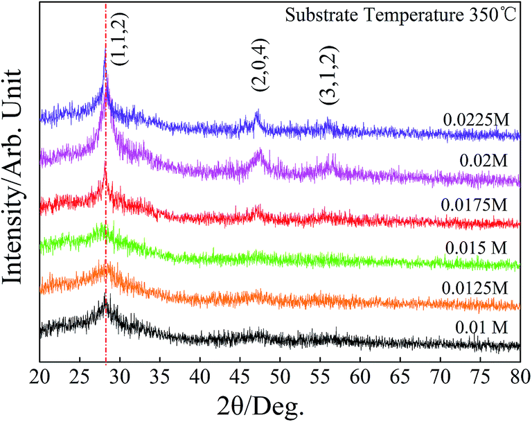 | ||
| Fig. 1 XRD patterns of the CTS thin films prepared by spray pyrolysis at different Cu concentrations in precursor solution. | ||
As literature reported,6–12,31 XRD patterns of the monoclinic and cubic CTS may similar to that of the tetragonal one (also list in the Table 1). Therefore, the Raman technology was applied to further confirm the microstructure of the prepared CTS thin film, and the result was shown in Fig. 2. The Raman spectrum shows peaks at 297 cm−1, 334 cm−1 and 351 cm−1 which match well with the tetragonal CTS.32 It was different from the peaks at 303 cm−1 and 355 cm−1 corresponding to cubic CTS also different from monoclinic CTS with the Raman spectra of the peaks at 287 cm−1, 290 cm−1 and 352 cm−1.11 As the arrow points in Fig. 2, there are also several weak peaks at 477 cm−1, 187 cm−1, 220 cm−1, 288 cm−1 which may be due to the characteristic peaks of CuxS33 and SnxSy.34 Therefore, it can be confirmed that the above-obtained CTS film prepared by spray pyrolysis route was tetragonal phase mixed with small amounts of Cu–S compounds and Sn–S compounds, as confirmed by XRD and Raman technologies.
| Phases | 2θ | I | hkl |
|---|---|---|---|
| Monoclinic | 28.41° | 100 | (![[1 with combining macron]](https://www.rsc.org/images/entities/char_0031_0304.gif) 31) 31) |
| 47.21° | 36 | (![[3 with combining macron]](https://www.rsc.org/images/entities/char_0033_0304.gif) 31) 31) |
|
| 56.07° | 22 | (![[4 with combining macron]](https://www.rsc.org/images/entities/char_0034_0304.gif) 02) 02) |
|
| Cubic | 28.45° | 100 | (111) |
| 47.31° | 48 | (220) | |
| 56.13° | 30 | (311) | |
| Tetragonal | 28.54° | 100 | (112) |
| 47.47° | 46 | (204) | |
| 56.32° | 28 | (312) |
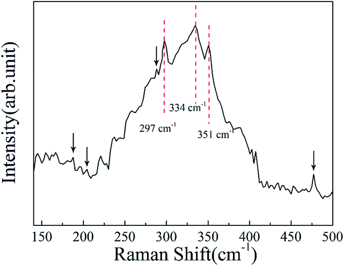 | ||
| Fig. 2 Raman spectra of the CTS thin film prepared at 350 °C. | ||
For analyzing the effects of the substrate temperature on the properties of the CTS thin films. The substrate temperature was varied from 325 °C to 400 °C with 25 °C increment, while keeping the Cu concentration at 0.02 M. The elemental composition of the obtained CTS thin film was analyzed by EDS. The stoichiometric ratios of the synthesized CTS were Cu1.30SnS2.39, Cu1.43SnS2.59, Cu1.63SnS2.60, and Cu1.25SnS2.27 under 325 °C, 350 °C, 375 °C and 400 °C, respectively. From the results shown, the average compositions of the thin films were considered to be Cu-poor and S-poor, which will benefits to the achievement of nondegenerate doping CuSnS3 films.35 Fig. 3 gives the Cu/Sn ratio as the function of substrate temperature, and the percentage of each element in CTS at different substrate temperature was shown in Table 2. According to Fig. 3, it could be observed that the value of Cu/Sn increased with the substrate temperature raised up to 375 °C, and then decreased with the temperature reached 400 °C. The changeover of Cu/Sn value may have relation with product of CuxS when the temperature was higher than 375 °C. The percentage of S generally decreased with the temperature raised from the optimal 350 °C to 375 °C and 400 °C as depicted in Table 2, which could be attributed to the volatility of S at high temperature.
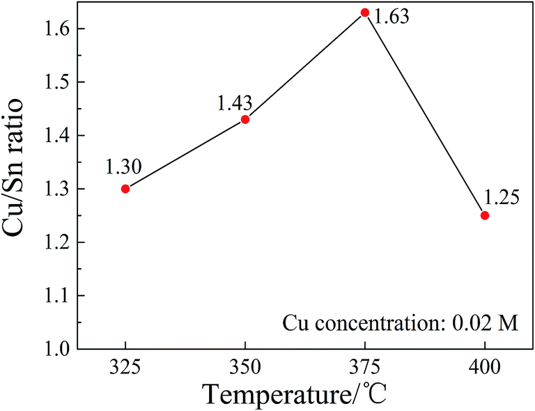 | ||
| Fig. 3 Variation of the Cu/Sn ratio as function of substrate temperature. | ||
| Temperature (°C) | Cu (%) | Sn (%) | S (%) |
|---|---|---|---|
| 325 | 27.81 | 21.24 | 50.95 |
| 350 | 28.33 | 19.88 | 51.79 |
| 375 | 31.23 | 19.05 | 49.73 |
| 400 | 27.92 | 23.23 | 49.84 |
The X-ray patterns of the CTS thin films prepared at various substrate temperatures is shown in Fig. 4(a). When the substrate temperature was in 325 °C and 350 °C, all the peaks at 28.540°, 47.474° and 56.326° are found to match well with that of the tetragonal Cu2SnS3 (JCPDF no. 89-4714) and they are identified to be reflections due to (1, 1, 2), (2, 0, 4) and (3, 1, 2) planes, respectively. The calculated lattice parameters of the CTS are a = 5.41 Å and c = 10.82 Å. These peaks become sharper with the temperatures of substrate increased from 325 °C to 350 °C, which is due to the improved crystallinity of CTS with higher temperature. However, the shift of the main peak to lower angle values and its intensity decreased dramatically when the temperature reached 375 °C. Corresponding to Table 1, the peaks shift phenomenon may attributed to the structure of CTS translated to cubic (JCPDF no. 89-2877) in 375 °C. The decreased intensity may be partly due to the decomposition of the synthesized CTS compound at high temperature. And with the temperature further increasing to 400 °C, the CTS structure changed to monoclinic (JCPDF no. 04-010-5719).8,10
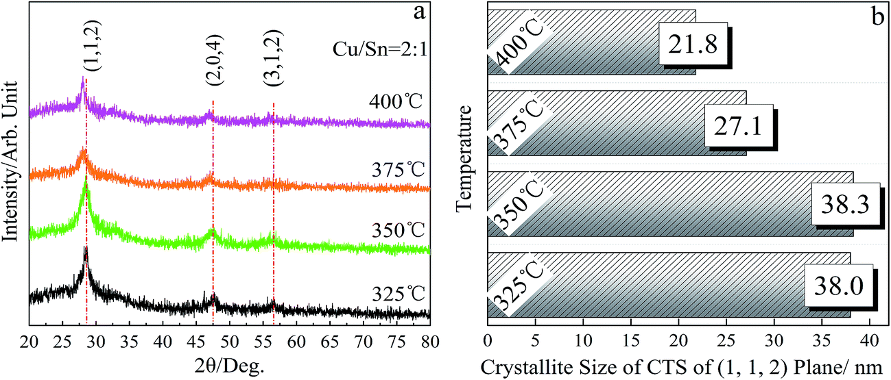 | ||
| Fig. 4 (a) XRD patterns of the CTS thin films prepared by spray pyrolysis at various substrate temperatures; (b) the crystallite size of the CTS nanocrystal calculated from (1, 1, 2) plane. | ||
The crystallite size (L) in these thin films is determined using Scherrer's formula36 where
Lhkl = kλ/β![[thin space (1/6-em)]](https://www.rsc.org/images/entities/char_2009.gif) cosθ cosθ | (1) |
L hkl is the diameter of the crystalline grain perpendicular to the direction of the (hkl) lattice plane, k is the Scherrer constant (usually 0.89), λ is the wavelength of Cu Kα (0.15406 nm), β is the full-width at half maximum (FWHM) and θ is the Bragg angle. The calculated crystallite size of the sprayed CTS from (1, 1, 2) plane was shown in Fig. 4(b). The crystallite size estimated for the standard (1, 1, 2) plane showed that crystallite increased as the substrate temperature raised from 325 °C to 350 °C, but it decreased with temperature further increased, which indicated the temperatures more than 350 °C are not propitious for further crystallization of CTS. Comparing with the sample obtained under 350 °C, the sample prepared at 375 °C has the following different phenomena. The intensity of the main peak decreased. The position of the main peak shifted left. And the Cu/Sn ratio of the prepared compound film increased. These phenomena indicated the secondary phase's products of CTS such as CuxS37 may be generated at this temperature. It can partly disrupted the further crystallization of the CTS, resulted into small crystallite size as described above.
The absorption spectrum at wavelengths of 500 nm to 1200 nm for the CTS thin films which was obtained in 325 °C to 400 °C and Cu concentration at 0.02 M were measured, and the result was shown in Fig. 5. In whole range of wavelength, the absorbance of CTS increased with the substrate temperature raised from 325 °C to 350 °C. However it decreased with the temperature further raised. The absorbance of CTS obtained at 350 °C is the highest which indicated the thin film prepared at this temperature has best optical adsorption properties. More photons would be absorbed in this CTS absorber layer, and therefore more excellent performance of photoelectric conversion is expected.
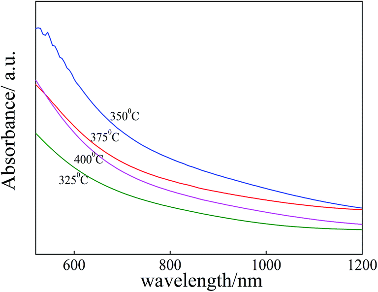 | ||
| Fig. 5 The absorption spectrum of CTS thin films by spray pyrolysis at different substrate temperatures. | ||
The feature of the absorption is determined using classical relation38 for absorption coefficient
| α = A(hν − Eg)n/hν | (2) |
The Tauc plot40 for the as-deposited CTS thin films is shown in Fig. 6, which is obtained by extrapolating the linear region of the (αhν)2 versus (hν) to the horizontal axis and consider the intersecting point. The Eg of sprayed CTS thin films are found to be 1.37 eV, 1.16 eV, 1.46 eV, 1.59 eV corresponding to the substrate temperature 325 °C, 350 °C, 375 °C, 400 °C, respectively. The CTS obtained in 325 °C found to reveal phases in tetragonal from XRD and Raman analyses, it has been reported on literature that bandgap of tetragonal structure is 1.35 eV. There are a few secondary phase's products like Sn2±xS (Eg: 1.6–1.9 eV), SnS2−x (Eg: 2.1–2.3 eV)30 and Cu2S41 (Eg: cubic: 0.4 eV hexagonal: 0.5 eV monoclinic: 0.6 eV) generated at higher temperature. The variation of CTS sample's band gap may be impacted by the crystal transition and above-mentioned secondary phases.42 The band gap of tetragonal CTS obtained at 350 °C was lower than 1.35 eV, which was most possibly influenced by the secondary phase of Cu2S. However, the band gap of 1.16 eV may be a more suitable candidate for high-efficiency multi-junction solar cells. As we know, low-band gap materials with proper value was used in multi-junction solar cells in order to maximally expand the spectral response of the multi-junction solar cells,43,44 and thus resulted into high efficiency. For example, if the CTS thin film with band gap of 1.16 eV obtained at optimal temperature of 350 °C is used as the third layer of multi-junction solar cells with (2.6 eV/1.8 eV/1.2 eV/0.8 eV) structure,23,45 high efficiency solar cell will be expected since the band gap value of 1.16 eV is very closed to the ideal value of 1.2 eV.
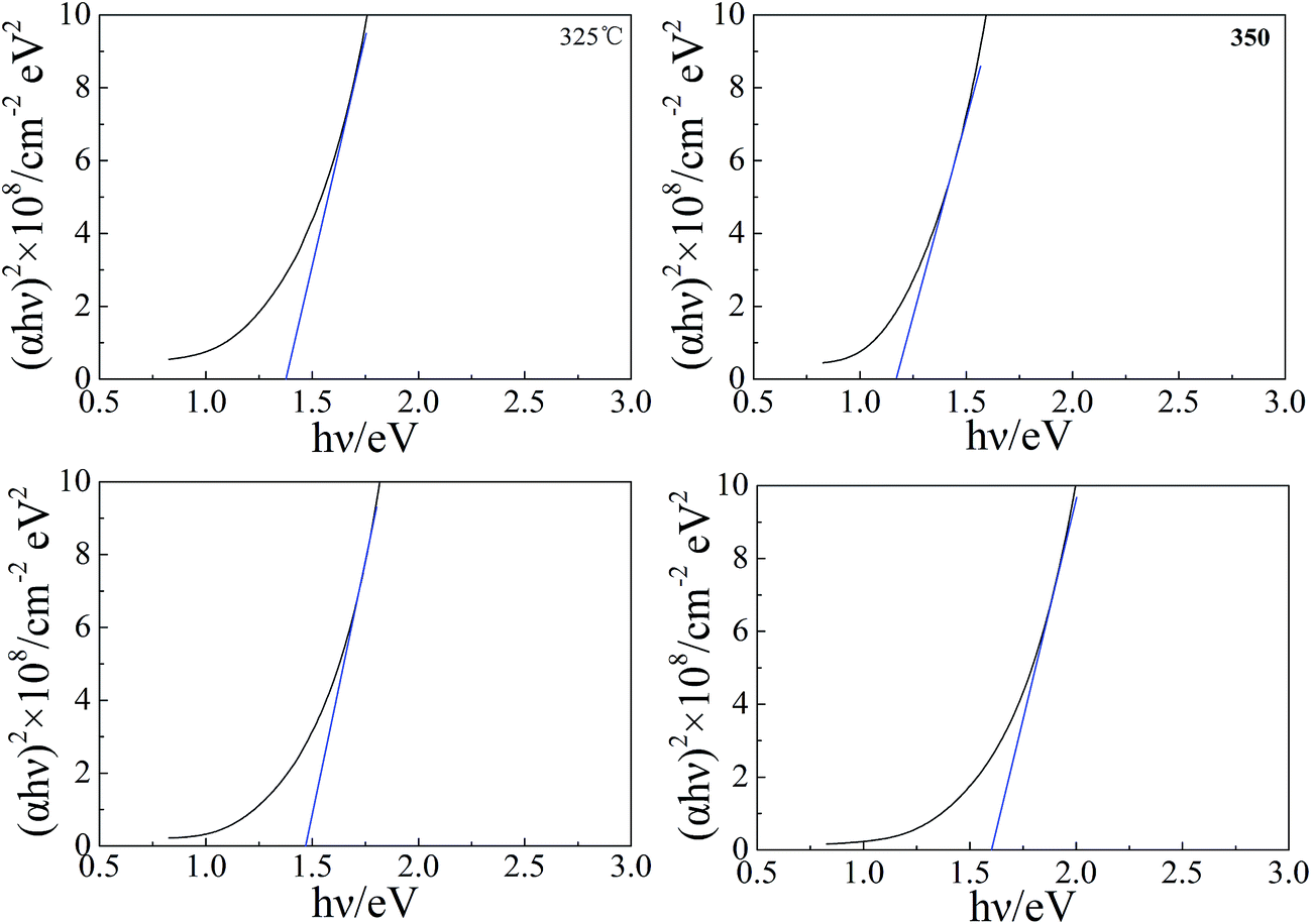 | ||
| Fig. 6 Tauc plot of CTS thin films obtained at different substrate temperatures. | ||
The electrical properties of the prepared CTS thin films were analyzed by Four-probe Resistivity Tester and the values of resistivity were shown in Fig. 7(a). It was observed that the CTS thin films prepared under 350 °C showed lowest resistivity of 11.6 × 10⁻² Ω cm, and the resistivity of the thin film increased when the temperature raised. According to Rodriguez-Lazcano,46 the resistivity of the thin film is related to its grain size. The effect of grain size on the resistivity47 can be due to the number of grain boundaries which have many crystal defects and impurities acting as scattering centers in the process of electron transmission. Therefore, the thin film with larger grain size has less grain boundaries, resulting into lower resistivity. Moreover, the resistivity of the film also relates to its thickness on a macro level according to Logan M. A.48 that resistivity is inversely proportional to thickness. It is obviously observed in the Fig. 7(b) that the thickness of the CTS thin films obtained at 350 °C was the thickest one, which would further contributed to its low resistivity. The thin film prepared at 350 °C with low resistivity can be benefit to the carrier mobility, and thus to the efficiency of the solar cell. The morphology of the thin film obtained at 350 °C were analyzed by SEM and AFM, and the result is shown in Fig. 8. Fig. 8(a) shows the cross section SEM image of the film, indicating the average thickness of film is around 1.1 µm, which match well to the result from the Fig. 7(b). Fig. 8(b) & (c) are the surface SEM & AFM images of the film. It was found that the height difference between the highest point and lowest point at the film surface is about 600–700 nm, consistent with the result from Fig. 8(a). Although the roughness of the prepared film is not so good at this stage, there are no any pinholes and cracks can be found in the SEM & AFM surface images, which is beneficial for further solar cell fabrication.
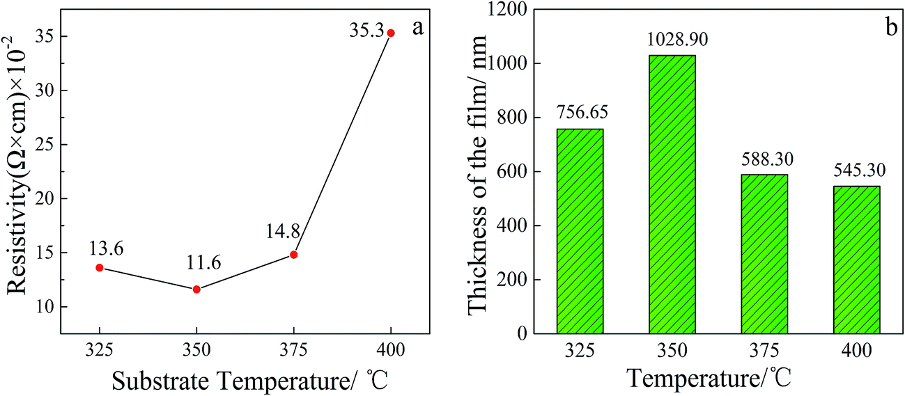 | ||
| Fig. 7 (a) The resistivity of CTS thin films obtained at different substrate temperatures; (b) the corresponding thickness of CTS thin films at different substrate temperatures. | ||
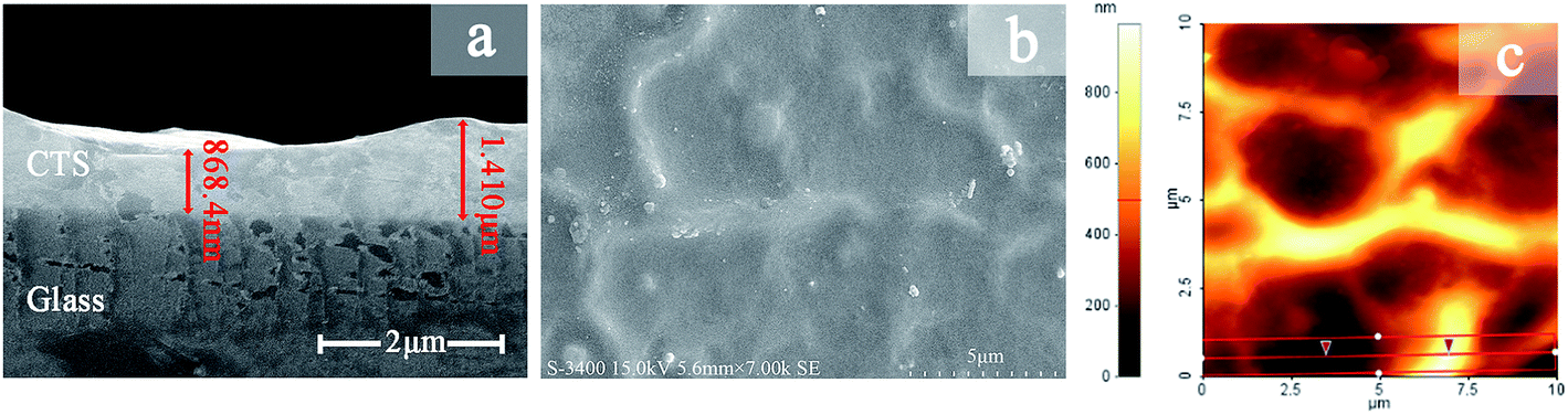 | ||
| Fig. 8 (a) The cross-sectional SEM image of CTS thin film; (b) surface SEM image of CTS thin film; (c) surface line-AFM image of CTS thin film. | ||
3. Conclusion
In this work, the ternary CTS compound thin films were successfully prepared on the glass substrate via a low-cost and simple spray pyrolysis method. The microstructure of the sprayed CTS film varied with the substrate temperature. The XRD pattern and Raman spectrum showed the single tetragonal CTS thin film obtained at the substrate temperature of 350 °C and Cu concentration in precursor solution of 0.02 M has the best crystallinity and the largest crystallite size of 38.3 nm. In this condition, the synthesized CTS was Cu-poor and S-poor with metal atomic ratio of Cu1.43SnS2.59, the resistivity was 11.6 × 10⁻² Ω cm, and the band gap value was 1.16 eV. These properties suggest that the sprayed CTS holds great potential in photovoltaic field and also is suitable for the high efficiency multi-junction solar cells.Acknowledgements
The project was supported by the Fundamental Research Funds for the Central Universities, China (no. WM1414047); Shanghai Committee of Science and Technology, China (no. 13JC1404300); Foundation for The Youth Scholars of Shanghai Municipal Education Commission, China (no. ZZSLG13013); Teachers' Innovation Ability Construction of University of Shanghai for Science and Technology, China (no. GDCX-Y-1205); Innovation Fund Project For Graduate Student of Shanghai, China (no. JWCXSL1301).References
- ZSW Brings World Record Back to Stuttgart New best mark in thin-film solar performance with 21.7 percent efficiency, http://www.zsw-bw.de/en/support/press-releases/press-detail/zsw-brings-world-record-back-to-stuttgart.html.
- D. A. R. Barkhouse, O. Gunawan, T. Gokmen, T. K. Todorov and D. B. Mitzi, Prog. Photovoltaics, 2012, 20, 6–11 CAS.
- K. Tanaka, M. Oonuki, N. Moritake and H. Uchiki, Sol. Energy Mater. Sol. Cells, 2009, 93, 583–587 CrossRef CAS PubMed.
- A. Nagoya, R. Asahi, R. Wahl and G. Kresse, Phys. Rev. B: Condens. Matter Mater. Phys., 2010, 81, 113202 CrossRef.
- N. Kitagawa, S. Ito, D.-C. Nguyen and H. Nishino, Nat. Resour., 2013, 4, 142 CAS.
- D. Tiwari, T. K. Chaudhuri, T. Shripathi, U. Deshpande and R. Rawat, Sol. Energy Mater. Sol. Cells, 2013, 113, 165–170 CrossRef CAS PubMed.
- M. Adelifard, M. M. B. Mohagheghi and H. Eshghi, Phys. Scr., 2012, 85, 035603 CrossRef.
- N. Aihara, H. Araki, A. Takeuchi, K. Jimbo and H. Katagiri, Phys. Status Solidi C, 2013, 10, 1086–1092 CrossRef CAS.
- M. Bouaziz, M. Amlouk and S. Belgacem, Thin Solid Films, 2009, 517, 2527–2530 CrossRef CAS PubMed.
- K. Chino, J. Koike, S. Eguchi, H. Araki, R. Nakamura, K. Jimbo and H. Katagiri, Jpn. J. Appl. Phys., 2012, 51, 10NC35 CrossRef.
- P. Fernandes, P. Salomé and A. da Cunha, J. Phys. D: Appl. Phys., 2010, 43, 215403 CrossRef.
- S. Fiechter, M. Martinez, G. Schmidt, W. Henrion and Y. Tomm, J. Phys. Chem. Solids, 2003, 64, 1859–1862 CrossRef CAS.
- T. A. Kuku and O. A. Fakolujo, International Society for Optics and Photonics, 1986, 321–325 CAS.
- D. M. Berg, R. Djemour, L. Gütay, G. Zoppi, S. Siebentritt and P. J. Dale, Thin Solid Films, 2012, 520, 6291–6294 CrossRef CAS PubMed.
- T. Nomura, T. Maeda and T. Wada, Jpn. J. Appl. Phys., 2013, 52, 04CR08 CrossRef.
- M. Konagai, Jpn. J. Appl. Phys., 2011, 50, 0001 CrossRef.
- J. Y. Kim, K. Lee, N. E. Coates, D. Moses, T.-Q. Nguyen, M. Dante and A. J. Heeger, Science, 2007, 317, 222–225 CrossRef CAS PubMed.
- T. Nomura, T. Maeda, K. Takei, M. Morihama and T. Wada, Phys. Status Solidi C, 2013, 10, 1093–1097 CrossRef CAS.
- Y. Kim, K. Kim, T. W. Kim, L. J. Mawst, T. F. Kuech, C. Z. Kim, W.-K. Park and J. Lee, Sol. Energy, 2014, 102, 126–130 CrossRef CAS PubMed.
- Q. Chen, X. Dou, Y. Ni, S. Cheng and S. Zhuang, J. Colloid Interface Sci., 2012, 376, 327–330 CrossRef CAS PubMed.
- W. Shockley and H. J. Queisser, J. Appl. Phys., 1961, 32, 510–519 CrossRef CAS PubMed.
- O. Höhn, T. Kraus, G. Bauhuis, U. T. Schwarz and B. Bläsi, Opt. Express, 2014, 22, A715–A722 CrossRef PubMed.
- A. De Vos, J. Phys. D: Appl. Phys., 1980, 13, 839 CrossRef.
- G. Cherucheril, S. March and A. Verma, in Multijunction Solar Cells, 2011 Search PubMed.
- K. Tanaka, Y. Fukui, N. Moritake and H. Uchiki, Sol. Energy Mater. Sol. Cells, 2011, 95, 838–842 CrossRef CAS PubMed.
- D. Avellaneda, M. Nair and P. Nair, J. Electrochem. Soc., 2010, 157, D346–D352 CrossRef CAS PubMed.
- A. Ennaoui, M. Lux-Steiner, A. Weber, D. Abou-Ras, I. Kötschau, H.-W. Schock, R. Schurr, A. Hölzing, S. Jost and R. Hock, Thin Solid Films, 2009, 517, 2511–2514 CrossRef CAS PubMed.
- G. Sunny, C. S. Kartha and K. Vijayakumar, Solid State Phys., Proc. DAE Solid State Phys. Symp., 2014, 1591(1), 1750–1752 CAS.
- L. Isac, I. Popovici, A. Enesca and A. Duta, Energy Procedia, 2010, 2, 71–78 CrossRef CAS PubMed.
- R. Engelken, H. McCloud, C. Lee, M. Slayton and H. Ghoreishi, J. Electrochem. Soc., 1987, 134, 2696–2707 CrossRef CAS PubMed.
- U. Chalapathi, Y. Jayasree, S. Uthanna and V. Sundara Raja, Phys. Status Solidi A, 2013, 210, 2384–2390 CrossRef CAS.
- D. Tiwari, T. K. Chaudhuri, T. Shripathi, U. Deshpande and V. Sathe, J. Mater. Sci.: Mater. Electron., 2014, 25, 3687–3694 CrossRef CAS.
- P. Fernandes, P. Salomé and A. Da Cunha, Thin Solid Films, 2009, 517, 2519–2523 CrossRef CAS PubMed.
- I. Parkin, L. Price, T. Hibbert and K. Molloy, J. Mater. Chem., 2001, 11, 1486–1490 RSC.
- L. L. Baranowski, P. Zawadzki, S. Christensen, D. Nordlund, S. Lany, A. C. Tamboli, L. Gedvilas, D. S. Ginley, W. Tumas and E. S. Toberer, Chem. Mater., 2014, 26, 4951–4959 CrossRef CAS.
- R. Jenkins and R. Snyder, Introduction to X-ray powder diffractometry, John Wiley & Sons, 2012 Search PubMed.
- P. S. McLeod, L. D. Partain, D. E. Sawyer and T. M. Peterson, Appl. Phys. Lett., 1984, 45, 472–474 CrossRef CAS PubMed.
- R. Salunkhe, U. Patil, T. Gujar and C. Lokhande, Appl. Surf. Sci., 2009, 255, 3923–3926 CrossRef CAS PubMed.
- A. Kokate, U. Suryavanshi and C. Bhosale, Sol. Energy, 2006, 80, 156–160 CrossRef CAS PubMed.
- J. Tauc, R. Grigorovici and A. Vancu, Phys. Status Solidi B, 1966, 15, 627–637 CrossRef CAS.
- P. Lukashev, W. R. Lambrecht, T. Kotani and M. van Schilfgaarde, Phys. Rev. B: Condens. Matter Mater. Phys., 2007, 76, 195202 CrossRef.
- J. I. Pankove, Optical processes in semiconductors, Courier Dover Publications, 2012 Search PubMed.
- E. Rao, A. Ougazzaden, Y. Le Bellego and M. Juhel, Appl. Phys. Lett., 1998, 72, 1409–1411 CrossRef CAS PubMed.
- J. Wu, W. Walukiewicz, W. Shan, K. Yu, J. Ager Iii, E. Haller, H. Lu and W. J. Schaff, Phys. Rev. B: Condens. Matter Mater. Phys., 2002, 66, 201403 CrossRef.
- M. Yamaguchi, T. Takamoto, K. Araki and N. Ekins-Daukes, Sol. Energy, 2005, 79, 78–85 CrossRef CAS PubMed.
- Y. Rodriguez-Lazcano, H. Martinez, M. Calixto-Rodriguez and A. Nunez Rodriguez, Thin Solid Films, 2009, 517, 5951–5955 CrossRef CAS PubMed.
- C. Durkan and M. Welland, Phys. Rev. B: Condens. Matter Mater. Phys., 2000, 61, 14215 CrossRef CAS.
- M. Logan, Bell Syst. Tech. J., 1967, 46, 2277–2322 CrossRef.
| This journal is © The Royal Society of Chemistry 2015 |