
Tuning the photoluminescence and ultrasensitive trace detection properties of few-layer MoS2 by decoration with gold nanoparticles
Shib Shankar Singha,
Dipanjan Nandi and
Achintya Singha*
Department of Physics, Bose Institute, 93/1, Acharya Prafulla Chandra Road, Kolkata 700 009, India. E-mail: achintya@jcbose.ac.in; Fax: +91 33 23506790; Tel: +91 33 23031177
First published on 24th February 2015
Abstract
We report an easy and inexpensive chemical route for the decoration of few-layer MoS2 with Au nanoparticles (NPs). The Au-NPs are formed on the defect sites of the MoS2 and localized by a non-covalent bond. The NPs act as a p-type dopant in the MoS2 layer. An enhancement in the photoluminescence (PL) intensity of the Au–MoS2 composite with respect to bare few-layer MoS2 has been observed. We also systematically observed a blue shift in the excitonic emission as the number and size of the Au-NPs on MoS2 increased. Both phenomena have been understood to result from the switching between charged exciton (trion) recombination and neutral exciton recombination. A potential application for the Au–MoS2 composite has been demonstrated, by using it as a substrate for surface-enhanced Raman scattering (SERS). The SERS measurements show a uniform, reproducible, and strong Raman signal from the adsorbed molecules with concentrations as low as 10−12 M. Our work provides a method to tune the optical and electronic properties of MoS2, and the Au–MoS2 composite might be useful as an efficient SERS substrate for the ultrasensitive detection of biomolecules.
Introduction
Layered transition metal dichalcogenides (LTMDs) have received much attention in recent years due to their remarkable optoelectronic properties.1–3 LTMDs are represented by the general formula of MX2, where M is an IVB, VB or VIB transition metal and X is sulphur, selenium, or tellurium.4 MoS2 belongs to the family of LTMDs. As a zero bandgap material, the uses of pristine graphene in the visible range of frequencies are constrained.5 In MoS2, the Mo layer is sandwiched between two hexagonal S layers. The atomic layers of MoS2 are held together by weak van der Waals forces and, due to this reason, layers can be exfoliated very easily with different techniques. Monolayer MoS2 is a direct bandgap semiconductor of energy ∼1.9 eV,3,6,7 and displays strong photoluminescence as a result.1,8 Therefore, monolayer MoS2 has been used in several optoelectronic applications, such as interband tunnel field effect transistors (FETs),9 photodetectors,10–12 photovoltaics13–15 and light emitters.3,16 In mono/few-layer MoS2, due to the presence of strong Coulomb interactions, optically generated electron–hole pairs form stable exciton states even at room temperature.17,18 Therefore, the carrier density plays an important role in determining the optical properties of mono/few-layer MoS2. Doping is one of the effective techniques to control the carrier density of monolayer TMDs.17–21 Among the different doping methods, such as the application of a gate bias voltage using a FET device,18–20 gas physisorption,21 etc., chemical doping is a simpler, cheaper and more convenient technique for controlling the carrier density of layered materials.17,22,23 Mouri et al.17 have shown an enhancement and reduction in the PL intensity when monolayer MoS2 is chemically doped by p-type and n-type dopants, respectively. It has also been reported that the Au-NPs attached at the edge sites of monolayer MoS2 act as a p-type dopant.24,25 However, Bhanu et al.25 have observed quenching of the PL in a Au–MoS2 hybrid structure, which is inconsistent with the result published in ref. 17. To understand the optoelectronic properties of MoS2 and Au-decorated MoS2, and consequently their possible applications, requires a careful investigation into their structure.In this work, few-layer MoS2 has been prepared from bulk MoS2 material by the well-known micromechanical cleavage or “scotch tape” method.1,26,27 A 0D–2D composite structure was synthesized by immersing the MoS2 in HAuCl4 solution. The Au-NPs (0D) were formed at the defect sites of MoS2 (2D) and the number and size of the Au-NPs increased with an increase in immersion time. The intensities of the excitonic emissions were enhanced as the Au-NPs started growing on the MoS2 layer. This observation has been attributed to the fact that the Au-NPs act as a p-type dopant, which reduces the number of intrinsic electrons in the bare sample and yields an increase in exciton recombination. In addition to that, the excitonic emission energies of the composite system are blue shifted compared to those of the bare MoS2, which is due to the increase in the Fermi energy by the dissociation of a charged exciton (trion). The stiffening of the E2g1 and softening of the A1g Raman modes with an increase in immersion time has been observed, which is consistent with an earlier report.28 The potential applicability of the Au–MoS2 hybrid structure has been examined by using it as a surface enhanced Raman scattering (SERS) substrate. Uniform and reproducible SERS signals have been observed at concentrations of Rhodamine 6G (R6G) dye as low as 10−12 M. The enhancement factor we have achieved is sufficient for the detection of single molecules. Hence, we conjecture that the optical properties of few-layer MoS2 can be tuned by decoration with Au-NPs and the Au–MoS2 hybrid structure can be utilized for ultrasensitive trace detection and might overcome the issues of low cross sections of Raman scattering.
Experimental section
Reagents
High purity bulk MoS2 was purchased from SPI Suppliers, gold(III) chloride tetrahydrate (HAuCl4, 4H2O) and Rhodamine 6G (R6G) were purchased from Sigma-Aldrich Pvt. Ltd. All chemicals were used as received without further purification. Milli-Q water was used during the entire synthesis and the experiments.Preparation of few-layer MoS2
Few-layer MoS2 flakes were prepared on a SiO2 (300 nm)/Si substrate using the micromechanical exfoliation technique.1,26 Before the deposition of flakes, the Si wafers were cleaned using piranha solution.Preparation of the Au–MoS2 hybrid structure
A 1 mM solution of HAuCl4 was prepared by mixing the proper amount of HAuCl4 with millipore water. Four different sets of samples were prepared by just varying the immersion time of the MoS2 flake-containing SiO2/Si substrate in the HAuCl4 solution for 30 min, 60 min, 90 min and 120 min and those samples were marked as S1, S2, S3 and S4, respectively.Preparation of the SERS substrate
A stock solution (10−3 M) of R6G was prepared with the desired volume of water and stored in a cold place. A wide range of solutions with different concentrations of R6G, from 10−5 to 10−12 M, was prepared from the stock solution. The sample S4 was used as the SERS substrate. The sample was immersed in the R6G solution for two hours, rinsed with Milli-Q water and then dried under nitrogen flow. Finally, SERS measurements were performed on the substrates with dye adsorbed. The same procedure was followed for all the other concentrations of R6G solutions.Instruments used for various characterization methods
SEM analysis was performed using an FEI Quanta 200 with an accelerating voltage of 30 kV. The Raman and PL measurements were performed using a micro Raman set-up consisting of a spectrometer (Lab RAM HR Jovin Yvon) and a Peltier cold CCD detector. An air cooled argon-ion laser (Ar+) with a wavelength of 488 nm and diode laser of wavelength 785 nm were used as an excitation light source, and a 100× objective with a numerical aperture (NA) of 0.9 was used to focus the laser on the sample and to collect the scattered light from the sample.Results and discussion
Fig. 1(a) shows the optical microscopy image of the MoS2 flake on the SiO2/Si substrate. The optical image has been taken using a 100× objective. The contrast in the area of the image marked by the red circle indicates that the few layers of MoS2 are present in that region. The number of layers has been confirmed using Raman spectroscopy. The Raman spectrum of the sample is displayed in Fig. 1(b). For reference, the Raman spectrum of bulk MoS2 is also presented. In MoS2, the E2g1 phonon mode originates from the displacement of the Mo and S atoms in the basal plane, whereas the A1g phonon mode is due to the vibration of the S atom in the opposite direction, along the direction perpendicular to the basal plane (see inset of Fig. 1(b)). The peak positions of the E2g1 and A1g modes are obtained from the fitting of the experimental curve using two Lorentzian functions. The Raman modes are highly sensitive to the thickness of the layer.27 In general, the gap between the E2g1 and A1g peaks decreases as the number of layers decreases.27 The gap for our MoS2 layer is found to be 24.97 cm−1, which ensures that the number of layers is less than 6.27 We have also performed PL measurements for further confirmation of the number of layers. Fig. 1(c) shows the PL spectra of bulk MoS2 (orange curve) and few-layer MoS2 (black curve). The large spin–orbit interaction in the few-layer MoS2 splits the highest valence band located at the K point of the Brillouin zone. Therefore, the direct optical transitions from the top of the spin-split valence bands to the bottom of the conduction band give A1 and B1 peaks.1 Both peaks are associated with exciton recombination. Additionally, the PL peak of the negative exciton (X−, trion) is also present in the micromechanically exfoliated MoS2 layer, because the layer unintentionally becomes n-type due to defects or the substrate effect.17,18,29 Therefore, we have fitted the PL spectrum using three Gaussian functions and the peak positions are at 1.80 eV, 1.86 eV and 1.96 eV, corresponding to X−, A1 and B1, respectively. The energy gap between X− and A1 is ∼60 meV, which is consistent with the value reported for monolayer MoS2.17,18,29 The intensity ratio of A1 and B1 is ∼1.3, which is in good agreement with the reported value for 4-layer MoS2,25 and confirms that the number of layers in our material is less than 6, as suggested by the Raman measurements.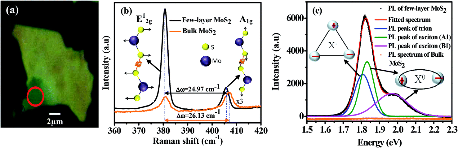 | ||
| Fig. 1 (a) Optical microscopy image of few-layer MoS2. The measurements have been performed at the place marked by the red circle. (b) Raman spectra of bulk (orange curve) and few-layer (black curve) MoS2. The schematic structures for the atomic displacements of the E2g1 and A1g modes are shown in the inset of the figure. (c) PL spectra of bulk (orange curve) and few-layer (black curve) MoS2. The red line is the result of a fit to the experimental data of few-layer MoS2 with three Gaussians functions for X− (blue), A1 (green), and B1 (magenta). The schematic structures of trion and exciton are shown in the inset. | ||
Scanning Electron Microscopy (SEM) images of Au–MoS2 hybrid structures (S2 and S4) are shown in Fig. 2(a) and (b), respectively. From the SEM images, it is clear that the number and size of the Au-NPs are greater in S4 than in S2, and no Au-NPs are observed on the bare SiO2 substrate. In MoS2, the defect sites are more reactive.24 The AuCl4− ions in the solution are initially attracted by the defect sites of the MoS2 and these act as nucleation centres for the growth of Au particles.24 So, with the increase in the immersion time, the number and dimensions of the Au-NPs increase, as observed in the SEM images.
 | ||
| Fig. 2 SEM images of (a) sample S2 and (b) sample S4. | ||
To investigate the role of Au agglomeration on MoS2, PL measurements were performed on the Au–MoS2 hybrid structure using an excitation wavelength of 488 nm. Fig. 3(a) shows the PL spectra of undoped MoS2 (black), S1 (red), S2 (blue), S3 (magenta) and S4 (dark yellow) samples. All of the spectra have been fitted with three Gaussian functions (for X−, A1 and B1). Fig. 3(b) shows the integrated intensity of the PL peaks as a function of the immersion time of MoS2 inside the HAuCl4. In the as-prepared sample, the PL intensity is higher for trions (X−) at an energy of 1.80 eV than the excitonic emission. This is because as-prepared MoS2 can unintentionally become n-type due to defects or the substrate effect,18,29,30 where trion recombination is dominant and the result is consistent with the earlier reports.17 The integrated intensities of the neutral excitonic peaks increased monotonically up to an immersion time of 60 min (sample: S3) and then decreased, whereas the integrated intensity of the trion peak remained almost constant. The experimental results are also consistent with earlier reports.17 This behaviour can be attributed to the fact that the electronic structure of MoS2 has been modified in the presence of the Au-NPs. Due to the difference in Fermi energy between MoS2 (4.7 eV)25 and Au (5.1 eV),25 a band bending takes place in the Au–MoS2 hybrid structure. Upon illumination with a photon of appropriate energy, an electron in the excited states of MoS2 transfers to Au leaving behind a hole, which acts as a p-dopant in MoS2. As a result, the number of excess carriers in the MoS2 layer is decreased and exciton recombination then predominates over the formation of trions. Moreover, the trions dissociate to excitons and one of the two electrons in the trion is unbound and placed in the Fermi level of the MoS2.18 Therefore, the number of excitons increases with an increase in the immersion time, which yields the enhancement in the intensity of the excitonic emission. Beyond 60 min, the PL intensity decreases because of the excessive p-doping. Fig. 3(c) shows that the PL energy shifts towards a higher energy with an increase in the immersion time of MoS2 in the HAuCl4 solution. As the exciton binding energy is large,18 neutral excitons emit more energy than trions. The increased number of neutral excitons yields the PL energy shift.29 The relative concentration of charged to neutral excitons can be estimated by the following expression.17,18,29
| γ = IX−/(IX0 + IX−) |
 | ||
| Fig. 3 (a) PL spectra of few-layer MoS2 obtained after different immersion times [S1 (30 min), S2 (60 min), S3 (90 min) and S4 (120 min)] inside the HAuCl4 solution. (b) Intensity and (c) energy of the X−, A1 and B1 peaks as a function of the immersion time. | ||
To gain a better understanding of how the adsorbed Au-NPs influence the vibrational mode, Raman measurements were performed on the Au–MoS2 hybrid structures. Fig. 4(a) shows the Raman spectra of all the samples, including as-prepared MoS2. The positions of the E2g1 and A1g modes as a function of the immersion time of MoS2 in the HAuCl4 solution are displayed in Fig. 4(b). The A1g mode shows a strong dependence on the immersion time, as the carrier concentration changes with immersion time, whereas E2g1 shows less dependence on the carrier concentration. We have observed softening and broadening of the A1g phonon mode as we increased the immersion time, which is due to the interaction of plasmons with A1g phonons. The maximum shift of the A1g mode is found to be 4 cm−1, which is consistent with the electron doped single layer MoS2 reported by Chakraborty et al.28 The gap between E2g1 and A1g phonon modes decreases with immersion time as shown in Fig. 4(c).
 | ||
| Fig. 4 (a) Raman spectra of few-layer MoS2 obtained after different immersion times [S1 (30 min), S2 (60 min), S3 (90 min) and S4 (120 min)] inside the HAuCl4 solution. (b) Variation of the E2g1 and A1g peak positions as a function of the immersion time and (c) the gap between the E2g1 and A1g modes as a function of the immersion time. | ||
To explore the utility of the metal–semiconductor composite system in ultrasensitive trace detection, the Au–MoS2 hybrid structures have been used as a substrate for a surface enhanced Raman spectroscopy (SERS) study. Two well-known effects are involved in SERS: the chemical and electromagnetic (EM) effects. The chemical effect originates from the charge transfer between the metal nanostructure and the molecule adsorbed on the metal surface. The localized electromagnetic field originating from the resonant coupling of the incident light with surface plasmons is the origin of EM effect. The EM effect is dominant in enhancing the Raman signal in the SERS phenomenon.31–38 The plasmonic coupling effects at the inter-particle gap in a cluster of noble metal particles provide a localized intense electromagnetic field, which is known as a hot spot. The Raman active molecules adsorbed at hot spots can be detected at the single-molecule level.31,39–46 A lot of effort has been focused on the preparation of stable metal clusters with small inter-particle gaps. DNA has been widely employed as a scaffold to produce specifically dispersed metal nanoparticles and to control the locations of these particles.47–52 Recently, metal nanoparticle-decorated graphene and graphene oxide have been used as efficient SERS substrates to detect molecules with concentrations in the nM range.53 In the present work, the Au-NPs are tightly immobilized by MoS2 and provide the abundant hot spots. R6G has been used as a Raman probe molecule. The normal Raman spectrum of solid R6G dye is presented in Fig. 5. The characteristic bands of R6G are observed at 609, 775, 1187, 1305, 1360, 1506, 1572 and 1648 cm−1. The peaks at 609 and 775 cm−1 are due to in plane xanthene ring deformation and out of plane C–H bending, respectively.54 The modes represented at 1187, 1305 and 1360 cm−1 are in plane xanthene ring deformation (C–H bending, N–H bending), in plane xanthene ring breathing (N–H bending, CH2 wagging) and in plane xanthene ring stretching (C–H bending), respectively.54 The bands at 1506, 1572 and 1648 cm−1 are related to in plane xanthene ring stretching (C–H bending, N–H bending and C–H stretching), in plane xanthene ring stretching (N–H bending) and in plane xanthene ring stretching (C–H bending), respectively.54
 | ||
| Fig. 5 Raman spectrum of solid R6G dye. The characteristic peaks of R6G are assigned. | ||
The SERS measurements were performed using the S4 sample and R6G solutions with concentrations of 1 × 10⁻⁵, 1 × 10⁻⁶, 1 × 10⁻⁹, and 1 × 10⁻¹² M. The SERS spectra at various concentrations recorded using 488 nm and 785 nm laser wavelengths are shown in Fig. 6(a) and (b), respectively. The normal Raman spectrum of R6G with 1 mM concentration (black curve) does not show any Raman bands. However, the Raman modes of R6G molecules on the Au–Mos2 substrate are clearly visible at concentration levels as low as 10−12 M. The enhancement is higher for a 488 nm laser than a 785 nm laser, which is expected, because the wavelength of the 785 nm laser is far from that of the plasmon resonance of the Au-NPs. To get a quantitative idea of the enhancement strength, the enhancement factor (EF) was calculated from the experimental data. The estimated value of the EF for the modes at 609, 1358, 1575 and 1648 cm−1 is ∼1010, which is sufficient for the detection of single molecules.52 We strongly believe that, in the future, the Au–MoS2 hybrid structure will be useful for the ultrasensitive detection of biomolecules and in other technologically important fields.
 | ||
| Fig. 6 Raman spectrum of 1 mM R6G solution (black) and the SERS spectra of R6G at concentrations of 1 × 10⁻⁵ M (red), 1 × 10⁻⁶ M (blue), 1 × 10⁻⁹ M (magenta), 1 × 10⁻¹² M (dark yellow) with the excitation wavelengths of (a) 488 nm and (b) 785 nm. The asterisk (*)-marked peaks are from MoS2 and the $-marked peak is from the Si substrate. | ||
Conclusions
In summary, we have presented a simple technique to realize a 0D–2D hybrid structure. The Au-NPs in this hybrid structure exhibit a p-doping effect on the MoS2. The hybrid structure has been studied systematically using PL and Raman measurements. We have demonstrated that the number and size of the Au-NPs play an important role in controlling the optical and vibrational properties of the MoS2. The excitonic emission properties are highly modified in the presence of Au-NPs, whereas the emission from trions is quite insensitive to their presence. The intensity and blue shift of the PL peaks have been understood to result from the conversion of trions to excitons under the illumination of the hybrid structure. We have also shown that the E2g1 phonon mode shows less dependence on the presence of Au-NPs compared to the A1g mode. Finally, we have utilized the hybrid structure as a potential SERS substrate for detection at the single molecule level. Hence, the Au-NP-decorated MoS2 can provide hybrid nanomaterials for applications in future digital electronics and sensors.References
- A. Splendiani, L. Sun, Y. Zhang, T. Li, J. Kim, Y. C. Chim, G. Galli and F. Wang, Nano Lett., 2010, 10, 1271–1275 CrossRef CAS PubMed.
- W. Zhao, Z. Ghorannevis, L. Chu, M. Toh, C. Kloc, P.-H. Tan and G. Eda, ACS Nano, 2013, 7(1), 791–797 CrossRef CAS PubMed.
- K. F. Mak, C. Lee, J. Hone, J. Shan and T. F. Heinz, Phys. Rev. Lett., 2010, 105, 136805 CrossRef.
- L. Yuwen, F. Xu, B. Xue, Z. Luo, Z. Qi, B. Bao, S. Su, L. Weng, W. Huang and L. Wang, Nanoscale, 2014, 6, 5762–5769 RSC.
- A. K. M. Newaz, D. P. J. I. Ziegler, D. Caudel, S. Robinson, R. F. Haglund Jr and K. I. Bolotin, Solid State Commun., 2013, 155, 49–52 CrossRef CAS PubMed.
- D. Gopalakrishnan, D. Damien and M. M. Shaijumon, ACS Nano, 2014, 8, 5297–5303 CrossRef CAS PubMed.
- G. Eda, H. Yamaguchi, D. Voiry, T. Fujita, M. Chen and M. Chhowalla, Nano Lett., 2011, 11, 5111–5116 CrossRef CAS PubMed.
- S. Tongay, J. Suh, C. Ataca, W. Fan, A. Luce, J. S. Kang, J. Liu, C. Ko, R. Raghunathanan, J. Zhou, F. Ogletree, J. Li, J. C. Grossman and J. Wu, Sci. Rep., 2013, 3, 2657 Search PubMed.
- S. Banerjee, W. Richardson, J. Coleman and A. Chatterjee, IEEE Electron Device Lett., 1987, 8, 347–349 CrossRef.
- Z. Yin, H. Li, L. Jiang, Y. Shi, Y. Sun, G. Lu, Q. Zhang, X. Chen and H. Zhang, ACS Nano, 2013, 6, 74–80 CrossRef PubMed.
- H. S. Lee, S. W. Min, Y. G. Chang, M. K. Park, T. Nam, H. Kim, J. H. Kim, S. Ryu and S. lm, Nano Lett., 2012, 12, 3695–3700 CrossRef CAS PubMed.
- O. Lopez-Sanchezl, D. Lembke, M. Kayci, A. Radenovic and A. Kis, Nat. Nanotechnol., 2013, 8, 497–501 CrossRef PubMed.
- J. Feng, X. Qian, C.-W. Huang and J. Li, Nat. Photonics, 2012, 6, 866–872 CrossRef CAS.
- M. Fontana, T. Deppe, A. K. Boyd, M. Rinzan, A. Y. Liu, M. Paranjape and P. Barbara, Sci. Rep., 2013, 3, 1634 Search PubMed.
- M. Bernardi, M. Palummo and J. C. Grossman, Nano Lett., 2013, 13, 3664–3670 CrossRef CAS PubMed.
- Y. Ye, Z. Ye, M. Gharghi, H. Zhu, M. Zhao, X. Yin and X. Zhang, Appl. Phys. Lett., 2014, 104, 193508 CrossRef PubMed.
- S. Mouri, Y. Miyauchi and K. Matsuda, Nano Lett., 2013, 13, 5944–5948 CrossRef CAS PubMed.
- K. F. Mak, K. L. He, C. Lee, G. H. Lee, J. Hone, T. F. Heinz and J. Shan, Nat. Mater., 2013, 12, 207–211 CrossRef CAS PubMed.
- J. S. Ross, S. Wu, H. Yu, N. J. Ghimire, A. M. Jones, G. Aivazian, J. Yan, D. G. Mandrus, D. Xiao, W. Yao and X. Xu, Nat. Commun., 2013, 4, 1474 CrossRef PubMed.
- A. M. Jones, H. Yu, N. J. Ghimire, S. Wu, G. Aicazian, J. S. Ross, B. Zhao, J. Yan, D. G. Mandrus, D. Xiao, W. Yao and X. Xu, Nat. Nanotechnol., 2013, 8, 634–638 CrossRef CAS PubMed.
- S. Tongay, J. Zhou, C. Ataca, J. Liu, J. S. Kang, T. S. Matthews, L. You, J. Li, J. C. Grossman and J. Q. Wu, Nano Lett., 2013, 13, 2831–2836 CrossRef CAS PubMed.
- W. Chen, S. Chen, D. C. Qi, X. Y. Gao and A. T. S. Wee, J. Am. Chem. Soc., 2007, 129, 10418–10422 CrossRef CAS PubMed.
- C. Coletti, C. Riedl, D. S. Lee, B. Krauss, L. Patthey, K. von Klitzing, J. H. Smet and U. Starke, Phys. Rev. B: Condens. Matter Mater. Phys., 2010, 81, 235401 CrossRef.
- Y. Shi, J. K. Huang, L. Jin, Y.-T. Hsu, S. F. Yu, L. J. Li and H. Y. Yang, Sci. Rep., 2013, 3, 1839 Search PubMed.
- U. Bhanu, M. R. Islam, L. Tetard and S. I. Khondaker, Sci. Rep., 2014, 3, 5575 Search PubMed.
- K. S. Novoselov, D. Jiang, F. Schedin, T. J. Booth, V. V. Khotkevich, S. V. Morozov and A. K. Geim, Proc. Natl. Acad. Sci. U. S. A., 2005, 102, 10451–10453 CrossRef CAS PubMed.
- C. Lee, H. Yan, L. E. Brus, T. F. Heinz, J. Hones and S. Ryu, ACS Nano, 2010, 4, 2695–2700 CrossRef CAS PubMed.
- B. Chakraborty, A. Bera, D. V. S. Muthu, S. Bhowmick, U. V. Waghmare and A. K. Sood, Phys. Rev. B: Condens. Matter Mater. Phys., 2012, 85, 161403 CrossRef.
- M. Buscema, G. A. Steele, H. S. J. V. Zant and A. Castellanos-Gomez, Nano Res., 2014, 7, 1–11 CrossRef CAS PubMed.
- H. Nan, Z. Wang, W. Wang, Z. Liang, Y. Lu, Q. Chen, D. He, P. Tan, F. Miao, X. Wang, J. Wang and Z. Ni, ACS Nano, 2014, 8, 5738–5745 CrossRef CAS PubMed.
- Q. Li, Y. Jiang, R. Han, X. Zhong, S. Liu, Z. Y. Li, Y. Sha and D. Xu, Small, 2013, 9, 927–932 CrossRef CAS PubMed.
- S. R. Emory, W. E. Haskins and S. Nie, J. Am. Chem. Soc., 1998, 120, 8009–8010 CrossRef CAS.
- H. Xu, J. Aizpurua, M. Käll and P. Apell, Phys. Rev. E: Stat. Phys., Plasmas, Fluids, Relat. Interdiscip. Top., 2000, 62, 4318–4324 CrossRef CAS.
- H. Xu, E. J. Bjerneld, M. Käll and L. Börjesson, Phys. Rev. Lett., 1999, 83, 4357–4360 CrossRef CAS.
- M. Moskovits, J. Raman Spectrosc., 2005, 36, 485–496 CrossRef CAS.
- K. A. Bosnick, J. Jiang and L. E. Brus, J. Phys. Chem. B, 2002, 106, 8096–8099 CrossRef CAS.
- A. Otto, J. Raman Spectrosc., 2002, 33, 593–598 CrossRef CAS.
- J. P. Camden, J. A. Dieringer, Y. Wang, D. J. Masiello, L. D. Marks, G. C. Schatz and R. P. Van Duyne, J. Am. Chem. Soc., 2008, 130, 12616–12617 CrossRef CAS PubMed.
- L. Yang, B. Yan, W. R. Premasiri, L. D. Ziegler, L. D. Negro and B. M. Reinhard, Adv. Funct. Mater., 2010, 20, 2619–2628 CrossRef CAS.
- M. Moskovits, Rev. Mod. Phys., 1985, 57(3), 783–826 CrossRef CAS.
- A. M. Michaels, J. Jiang and L. Brus, J. Phys. Chem. B, 2000, 104, 11965–11971 CrossRef CAS.
- Z.-Q. Tian, B. Ren and D.-Y. Wu, J. Phys. Chem. B, 2002, 106, 9463–9483 CrossRef CAS.
- A. Tao, F. Kim, C. Hess, J. Goldberger, R. He, Y. Sun, Y. Xia and P. Yang, Nano Lett., 2003, 3, 1229–1233 CrossRef CAS.
- K. A. Willets and R. P. V. Duyne, Annu. Rev. Phys. Chem., 2007, 58, 267–297 CrossRef CAS PubMed.
- F. Le, D. W. Brandl, Y. A. Urzhumov, H. Wang, J. Kundu, N. J. Halas, J. Aizpurua and P. Nordlander, ACS Nano, 2008, 2, 707–718 CrossRef CAS PubMed.
- F. J. G. Vidal and J. B. Pendry, Phys. Rev. Lett., 1996, 77, 1163–1166 CrossRef.
- S. J. Tan, M. J. Campolongo, D. Luo and W. Cheng, Nat. Nanotechnol., 2011, 6, 268 CrossRef CAS PubMed.
- S. Pal, R. Varghese, Z. Deng, Z. Zhao, A. Kumar, H. Yan and Y. Liu, Angew. Chem., Int. Ed., 2011, 50, 4176 CrossRef CAS PubMed.
- W. Guo, J. Yuan, Q. Dong and E. Wang, J. Am. Chem. Soc., 2010, 132, 932 CrossRef CAS PubMed.
- A. V. Gourine, E. Llaudet, N. Dale and K. M. Spyer, Nature, 2005, 436, 108–111 CrossRef CAS PubMed.
- L. Berti and G. A. Burley, Nat. Nanotechnol., 2008, 3, 81–87 CrossRef CAS PubMed.
- D. Majumdar, A. Singha, P. K. Mondal and S. Kundu, ACS Appl. Mater. Interfaces, 2013, 5, 7798–7807 CAS.
- G. Lu, H. Li, C. Liusman, Z. Yin, S. Wua and H. Zhang, Chem. Sci., 2011, 2, 1817–1821 RSC.
- L. Jensen and G. C. Schatz, J. Phys. Chem. A, 2006, 110(18), 5973–5977 CrossRef CAS PubMed.
| This journal is © The Royal Society of Chemistry 2015 |