M. K. Punith Kumar,
Monika Nidhi and
Chandan Srivastava*
Dept. of Materials Engineering, Indian Institute of Science (IISc), Bangalore-560012, India. E-mail: csrivastava@materials.iisc.ernet.in; Tel: +91-80-22932834
First published on 2nd March 2015
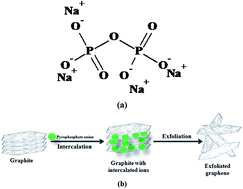
An electrochemical exfoliation based synthetic methodology to produce graphene is provided. An eco-friendly and non-toxic tetrasodium pyrophosphate solution in which the pyrophosphate anion acts as an intercalating ion was used as the electroactive media. Five different ion intercalation potentials were used. Characterization by microscopy, X-ray diffraction, Raman spectroscopy and UV-Visible spectroscopic techniques confirmed that all the potentials produced nano to micrometer sized graphene sheets. No trace of graphene oxide was detected. It was observed that (i) an increase in the intercalation potential increased the graphene yield and (ii) the defect density of graphene did not change significantly with a change in the intercalation potential.
In the present work, we employed electrochemical exfoliation process to produce graphene from a graphite electrode. The electrochemical process derives its merit from the facts that it is a low cost, eco-friendly and non-equipment intensive technique.15,16 Both anodic and cathodic electrochemical exfoliation processes are currently widely used to produce graphene by electrochemical exfoliation method.16,17 Based on the ionic size and intercalating property, many organic and inorganic molecules are used to exfoliate graphite.18 Gu et al.19 have proposed a high throughput method of producing high quality graphene sheets by liquid phase exfoliation of worm like exfoliated graphite using concentrated sulphuric acid and hydrogen peroxide.19 Use of sulphate based compounds like sulphuric acid or inorganic sulphate salts leads to intercalation of sulphate anion within the carbon layers in graphite. Ionic size of the SO42− anion is 0.46 nm which is larger than the interlayer spacing between the graphitic layer i.e., 0.335 nm.20 The intercalated SO42− ion therefore weakens the bond between the graphitic layers and leads to the exfoliation of graphite into separate graphene layers. Majority of the intercalating molecules like acids, bases and ionic liquids which are being used however are highly aggressive, corrosive and eco-toxic in nature. In the interest of environment and personnel safety, use of these molecules therefore should be discouraged both in laboratory and industrial scale processes that produce graphene. Hence, there exists a need for identifying and developing exfoliation processes that employ eco-friendly and non-toxic molecules. Some “green” approaches to produce graphene-based materials have already been reported in the literature. In one of the approaches, Parvez et al.21 have electrochemically exfoliated graphite using aqueous inorganic salt solutions like ammonium sulphate, sodium sulphate and potassium sulphate to produce highly conductive graphene layers.21 In yet another approach, Lee et al.22 have anodically exfoliated graphite in poly(sodium-4-styrenesulfonate) electrolyte using simple DC source and demonstrated the influence of exfoliated graphene on enhancement of electrochemical performance of Li ion battery electrodes.22
Here we demonstrate the use of non-toxic tetrasodium pyrophosphate (TSPP) compound as an electroactive media to exfoliate graphite rod at different intercalation potentials to produce graphene. Pyrophosphate ion is non-toxic and biocompatible.23,24 It is common in sea food, tooth paste and is extensively used as a food additive. Structure of Tetrasodium pyrophosphate (TSPP) is shown in Fig. 1(a). Tetrasodium pyrophosphate anion leads to anodic exfoliation process because of the intercalation of bulky pyrophosphate anion molecule within the graphitic layers. Intercalation induces strain between the layers and expands the graphite anode facilitating exfoliation as illustrated in Fig. 1(b).
![]() | ||
Fig. 1 (a) Structures of Tetrasodium pyrophosphate (TSPP) molecule and (b) a schematic showing the mechanism of graphene exfoliation in presence of TSPP. |
X-ray diffraction (XRD) profiles from graphene samples deposited on glass substrate were obtained by using X-pert pro X-ray diffractometer employing a Cu Kα radiation (λ = 0.1540 nm) source. Raman spectrums from the exfoliated samples were obtained using microscope setup (HORIBA JOBIN YVON, Lab RAM HR) consisting of Diode-pumped solid-state laser operating at 532 nm with a charge coupled detector. UV-Visible absorption spectroscopic experiments were carried in 700 to 200 nm wavelength range using Perkin Elmer (Lambda 35) UV-Vis Spectrometer. Scanning electron micrographs of graphene samples prepared on silica substrate were acquired using JOEL-JEM-1200-EX II Scanning electron microscope (SEM) operating at 20 kV. A 300 keV field emission FEI Tecnai F-30 transmission electron microscope (TEM) was used for obtaining TEM bright field images of exfoliated graphene samples. Samples for the TEM based analysis were prepared by drop drying graphene dispersion on a carbon coated copper grid. Atomic force microscopy (AFM) experiments were carried at room temperature using Nanosurf AFM instrument (Switzerland). Graphene–ethanol dispersion was drop dried over silica substrate for the AFM based analysis.
![]() | ||
Fig. 2 X-ray diffraction profiles obtained from graphite and graphene exfoliated at different intercalation potential. |
The absorption of UV-Vis light depends on the functional groups present in the materials being investigated hence UV-Vis absorption spectroscopy is a useful tool to distinguish between graphene and graphene oxide which basically differ in functionalities attached to the parental carbon structure. The recorded UV-Vis spectra for the exfoliated graphene samples are shown in Fig. 3(a). The maximum absorption (λmax) at 270 nm which corresponds to π → π* transition of the aromatic C–C bonds in graphene was observed for all the exfoliated samples. The absence of graphene oxide characteristic absorption peak around 230 nm confirmed that all the exfoliated samples contained only reduced graphene sheets.16,27 The insert in Fig. 3(a) clearly shows the absence of peak ∼230 nm. The absence of graphene oxide peak in Fig. 3(a) supports the XRD results about the presence of negligible amount of graphene oxide in the exfoliated sample. It can be observed in Fig. 3(a) that the absorption intensity is increased with increase in the exfoliation potential. It should be noted that equal volumes of the ethanol dispersion of graphene from different exfoliation experiments were used for the UV-Vis absorption measurement. The variations in absorption intensity therefore clearly illustrates that the concentration of graphene in the suspension and thus its yield depends on the voltage that was used for the exfoliation process. In order to determine the concentration of exfoliated graphene samples, the absorption coefficient (α) was first determined experimentally. Absorption coefficient is an important parameter in characterizing concentration using the Lambert–Beer law28 (A/l = αC where, A is absorption peak intensity; l is path length; C is concentration and α is the absorption coefficient). Graphene dispersions in ethanol with known concentrations were prepared. Absorbance per unit path length was then measured at λ660 nm. Relationship between absorption per unit length and known graphene concentrations is shown as a plot in Fig. 3(b). Slope of the straight line fit through the data points in Fig. 3(b) provided the absorption co-efficient value of α = 2421 ml mg−1 m−1. This absorption coefficient value was then used to determine the unknown concentration of the graphene dispersions obtained from different exfoliation experiments using the Lambert–Beer law and the value of absorption per unit length at λ660 nm in the UV-Vis profiles in Fig. 3(a). Concentration of graphene in the exfoliated dilute graphene dispersions were found to be 9.87 μg ml−1, 11.18 μg ml−1, 12.54 μg ml−1, 17.67 μg ml−1 and 23.57 μg ml−1 for 3 V, 4 V, 5 V, 6 V and 7 V respectively. Therefore an increase in the exfoliation potential increased the yield of graphene.
Raman spectra obtained from graphite and electrochemically exfoliated samples are given in Fig. 4(a). The Raman spectra of all the samples revealed three major peaks: D band at ∼1361 cm−1 corresponding to sp3 defects, G band around ∼1580 cm−1 corresponding to the phonon mode in-plane vibration of sp2 carbon atoms and 2D band at ∼2700 cm−1 corresponding to the two phonon lattice vibration.27,29,30 A slight shift in the 2D band position of the exfoliated samples towards lower wave number as compared to the 2D peak position of graphite and a considerable intensity of the 2D peak observed in Raman spectra of exfoliated samples as shown in Fig. 4(b) collectively confirmed the presence of few layer graphene in the exfoliated samples.26 The intensity ratio between D and G peak i.e., ID/IG gives the defect density of the graphitic structure.30 The ID/IG ratios of graphite and graphene samples produced at different intercalation voltages are tabulated in Table 1. It is apparent from Table 1 that the defect density ratio of graphene did not differ significantly from the defect density of the graphite rod from which it was exfoliated for all the exfoliation potentials and the exfoliation potential also did not significantly effect on the defect density of the exfoliated product. One important observation that can be made from the Fig. 4(a) is the appearance of a shoulder near 1615 cm−1 in the G-band peak as illustrated in Fig. 4(c) which plots the fitted curves obtained after de-convolution of the G-band peak and its shoulder. This shoulder peak is identified as the D′ band. It has been shown that this peak appears in few-layer graphene and is due to the presence of defects in the sp2 carbon lattice.31–33 D′ peak has also been reported for metallic CNT samples with defects.34 Relative difference in the intensity of the D′ peak between the graphene samples exfoliated at different voltages indicates towards the effect of exfoliation potential on the defects in the sp2 carbon lattice of the graphene samples.
Sample | G | 3 V | 4 V | 5 V | 6 V | 7 V |
---|---|---|---|---|---|---|
ID/IG | 0.9719 | 0.9754 | 1.0740 | 0.9962 | 0.9964 | 1.0707 |
Representative SEM images of graphene samples dispersed over silica wafer are shown in Fig. 5. The SEM micrographs reveal large, irregular and well separated graphene sheets with dimensions from nano to micron scale. Representative TEM bright field image of exfoliated graphene samples are shown in Fig. 6. TEM images clearly reveal the presence of isolated few layer graphene sheets in the exfoliated samples. Thickness of the exfoliated graphene sheets was investigated using the AFM technique. Representative AFM topographical images of graphene sheets exfoliated at different voltages is shown in Fig. 7. The Z-height profiles obtained from AFM images revealed that the graphene flakes exfoliated using 3–7 V had a thickness of 5 ± 2.3 nm, 4.5 ± 1.3 nm, 5.9 ± 1.0 nm, 6.3 ± 0.9, 5.7 ± 1.5 nm respectively. This result illustrated that the as-exfoliated samples contained few layer graphene sheets for all the exfoliation voltages. TEM and AFM images and thickness measurement results additionally illustrated that the as-synthesized graphene sheets were not agglomerated.
![]() | ||
Fig. 6 TEM bight field micrographs of graphene prepared by electrochemical exfoliation process at different intercalation potential. |
![]() | ||
Fig. 7 AFM topographical images of graphene synthesized at 3 V, 4 V, 5 V, 6 V and 7 V intercalation potential. |
This journal is © The Royal Society of Chemistry 2015 |