Fast and low-temperature synthesis of one-dimensional (1D) single-crystalline SbSI microrod for high performance photodetector

Guihuan Chenabcd, Wei Liabcd, Yongqiang Yuabcd and Qing Yang*abcd
aHefei National Laboratory of Physical Sciences at the Microscale, University of Science and Technology of China, Hefei 230026, Anhui, P. R. China. E-mail: qyoung@ustc.edu.cn; Fax: +86-551-63606266; Tel: +86-551-63600243
bDepartment of Chemistry, University of Science and Technology of China, Hefei 230026, Anhui, P. R. China
cLaboratory of Nanomaterials for Energy Conversion, University of Science and Technology of China, Hefei 230026, Anhui, P. R. China
dSynergetic Innovation Center of Quantum Information & Quantum Physics, University of Science and Technology of China, Hefei 230026, Anhui, P. R. China

Received 20th January 2015 , Accepted 19th February 2015

First published on 19th February 2015


Abstract

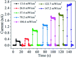
A new rapid and low temperature hydrothermal process has been developed to synthesize one-dimensional (1D) single-crystalline SbSI microrods at 160 °C for 4 h with high quality. Moreover, a first individual SbSI microrod based photodetector equipped with indium–tin-oxide (ITO) electrodes is constructed on a SiO2/Si substrate. The resulting device displays a remarkable response to visible light with an on–off ratio up to 727, a detectivity of 2.3 × 10⁸ Jones, a noise equivalent power of 1.7 × 10⁻¹⁰ W/Hz1/2 and fast response/recovery times (<0.3 s).


Photoconductivity is a very important property of semiconducting materials which originates from the photogeneration carrier under incident radiation. Photodetectors in the visible-light and/or UV region show extensive applications in sensors, imaging techniques, optical communications, and biological research.1 Up to date, most of the reported photodetectors are based on elemental silicon, III–V, II–VI, III–VI and V–VI compounds.2 Recently, ternary component compounds have demonstrated their special advantages to be high performance photodetectors,3 which imply that ternary component semiconductors may provide new opportunities for next generation opto-electronic devices.

Antimony sulfoiodide (SbSI) is a ferroelectric semiconductor material, which belongs to the V–VI–VII class of compounds and draws considerable attention due to its high dielectric, piezoelectric, and photoconducting properties.4,5 It is highly anisotropic orthorhombic phase structure which consists of infinite ribbon-like SbSI polar chains linked together and extend along c-axis, making its crystal preferentially to grow into one-dimensional (1D) structure anisotropically.6 Being a promising material with potential applications, the 1D SbSI crystals with various dimensions have been synthesized in different ways such as vapor deposition, sonochemical and hydrothermal routes.4,7–12

As noted, chemical vapor deposition (CVD) is available for the growth of poly-crystalline bulk from their corresponding elements at temperature over 600 °C,7 and sonochemical process can produce SbSI at a relative low temperature below 100 °C while the surface of the as-grown nanocrystals often shows an amorphous layer.8 Among the reported synthetic ways, hydrothermal processes have been widely used for the growth of such sulfoiodide compound crystals due to their advantages of low cost and simple operation in the procedures. However, it is noted that the hydrothermal processes for the synthesis of the 1D SbSI crystals usually need high reaction temperature over 250 °C in addition to extra high pressure in previous investigations.9 In our early work, we modified a hydrothermal route for the growth of the SbSI crystals from precursors of SbCl3, (NH2)2CS with NaI in a Teflon-lined stainless steel autoclave at 200 °C for long reaction time (>20 h),10 and it is occasionally noted that unwashed Teflon-lined container which was soaked by aqua regia is favorable for the growth of the SbSI crystals with relative high purity while we were not fully aware of the effect of residue acid at that time. Meanwhile, another modification was also available for the growth of the SbSI crystals from sources of SbCl3, (NH2)2CS with excessive elemental iodine and it was interesting that the reaction conditions could be reduced to 180–190 °C for 8–10 h.11 Since then, there have not been any investigations reported on the synthesis of SbSI crystals via hydrothermal fabrication routes until recent years. Motivated by and adopted from the above study, Sohn and coworkers have performed a hydrothermal process until recent years for the synthesis of 1D rod-shape SbSI crystals with lengths of sub-millimeters and widths of sub-microns, and characterized the thermogravimetric property of the as-grown crystals in detail.12

The photoelectric property of SbSI has been studied as early in 1958,13 and it is confirmed that bulk SbSI has a band gap from 1.82 to 1.84 eV at about 300 K,12,14 which would be available for promising photodetection at least in visible light region. However, to the best of our knowledge, the photoresponse performance of a photodetector based 1D SbSI crystal has not been studied in detail so far. In the present work, we successfully demonstrate an alternative facile hydrothermal synthetic route for the growth of 1D crystalline SbSI with high quality from sources of SbCl3, (NH2)2CS and NH4I in HCl aqueous solution at 160 °C for only 4 h via modifying our early work. It is interestingly found that the current process is highly efficient and low-cost for large scale synthesis of the SbSI single crystals in a facile and easily conducted way. Furthermore, the as-obtained SbSI crystals have complementary absorption spectra in visible-light and UV spectrum, which plays a key role in improving the sensitivity of the photoelectric devices. Importantly, a photodetector based on an individual SbSI microrod equipped with ITO contacts is firstly fabricated on a SiO2/Si substrate. Measurements reveal that the device displays a remarkable response to visible light with an on–off ratio up to 727, and exhibits a detectivity of 2.3 × 10⁸ Jones, a noise equivalent power of 1.7 × 10⁻¹⁰ W/Hz1/2, short response/recovery times (<0.3 s) and high stability. These results, for the first time, demonstrate the excellent photoresponse property of the SbSI crystals and imply their potential application in highly efficient low-cost light detection and signal magnification.

In the current syntheses, all reagents and solvents are of analytical purity and they were obtained from commercial sources with analytical grade and used without further purification. In a typical synthesis, 4.20 mmol (0.96 g) of SbCl3, 4.20 mmol (0.32 g) of (NH2)2CS and 21.00 mmol (3.05 g) NH4I were added into the Teflon-lined stainless steel autoclave which was filled up with 30 mL HCl aqueous solution (1.0 mol L−1). Then, the autoclave was maintained at 160 °C for 4 h. After reaction, the autoclave was cooled down to room temperature naturally. The resulting precipitates were washed with distilled water and ethanol several times. It is noted that the production can be magnified as demanded by using increased feedstock in a large-size autoclave in a singular batch.

The as-prepared products were characterized by X-ray powder diffraction (XRD) patterns on a Philips X' Pert Pro Super diffractometer with graphite-monochromatized Cu Kα radiation (λ = 1.54178 Å). The morphology, structure and composition of the products were investigated by the field emission scanning electron microscopy (SEM) (JEOL JSM-6700F), X-ray photoelectron spectroscopic (XPS) spectra was collected using a VGESCA-LAB MKII X-ray photoelectron spectrometer fitted with a monochromatic Al Kα X-ray source (1487 eV) operating on a spot size of 560 μm. UV-vis-NIR absorption spectra were recorded on a Perkin Elmer Lambda 950 UV-Vis-NIR spectrophotometer.

Photoresponse behavior of the SbSI was determined on the basis of a SiO2/Si substrate, fabricated as follows. An individual SbSI microrod (with lengths of ∼3.6 mm and diameters of 100 μm) was flattened on the SiO2 (300 nm)/p-Si (resistivity: <0.01–0.05 Ω cm), then, two ITO glasses (with the size 1 × 2 cm) were pressed against the SbSI with a parallel spacing of 1.5 mm. The current–voltage (IV) characteristics and the sensitivity of the photodetectors were measured using CHI600E electrochemical workstation, equipped with a xenon lamp of PLS-SXE300/PLS-SXE300UV with output wavelength range 400–780 nm. The influence of gate voltage on photoconductivity was performed by a semiconductor parameter analyzer system (Keithley 4200-SCS) at room temperature.

Fig. 1 presents a typical XRD pattern of the as-prepared 1D SbSI crystal (top) and the corresponding standard Joint Committee on Powder Diffraction Standards (JCPDS) Card no. 88-0988 (bottom). All diffraction peaks in the pattern are labeled and they present clear evidence for that the products are composed of one pure orthorhombic phase antimony sulfoiodide with a space group Pnma. It is worth noting that the diffraction peaks of (120), (310), (330) and (150) facets are more intensive than they would be in the standard card, which implies that the crystalline SbSI grow preferentially along c-direction. Meanwhile, the intense diffraction peaks imply the high quality of the as-prepared SbSI crystals.


image file: c5ra01180a-f1.tif
Fig. 1 XRD patterns of the samples synthesized at 160 °C for 4 h in 1.0 mol L−1 hydrochloric acid (top) and standard data of JCPDS Card no. 88-0988 (bottom).

Fig. 2a and b show the representative low- and high-magnification SEM images of the SbSI samples. It is observed that the samples have rod-like shape and smooth surface with lengths of several millimeters and diameters of several tens microns. Fig. 2c displays a photograph of the samples which present dark red color with crystal luster, suggesting high crystallinity of the 1D SbSI microcrystals. Fig. 2d demonstrates the schematic crystal structure of the microrods with a top view of (001) (left) and the chain-like building blocks of SbSI along c-axis. Meanwhile, XPS measurement is performed to reveal the compositional and chemical state of the microrods. Fig. 3a illustrates the survey spectrum for the microrods. It is observed that, the peaks arising from SbSI (Sb 4d, 3d, 3p and Sb MNN Auger, S 2p, 2s and I 4d, 3d, 3p, and I MNN Auger) are readily apparent.10,15 In details, the antimony high-resolution XPS spectrum at 529.8 and 539.2 eV (Fig. 3b), the sulfur 2p peaks at 161.8 eV and 162.8 eV (Fig. 3c), and the iodine 3d binding energy at 619.0 eV and 630.5 eV (Fig. 3d) are all consistent with those previously observed in SbSI.10,15,16


image file: c5ra01180a-f2.tif
Fig. 2 (a) Low- and (b) high-magnification SEM images, (c) a photograph of the final obtained SbSI crystals, and (d) scheme of crystal structure: (001) (left) and (010) plane (right) of a SbSI crystal.

image file: c5ra01180a-f3.tif
Fig. 3 (a) XPS survey spectrum, (b) high-resolution Sb 3d, (c) S 2p and (d) I 3d core level regions for the SbSI microrods.

Fig. 4 displays SEM images of the samples synthesized in different concentration of hydrochloric acid solution with other experimental conditions unchanging. It is found that when the concentration of hydrochloric acid solution is 0.4 mol L−1, the produced sample is mainly SbSI crystals (JCPDS Card no. 88-0988) mixed with small amount of orthorhombic Sb2S3 (JCPDS Card no. 73-0393) (Fig. S1). They demonstrate as sheaf-like assemblies of bundles with some small particles (Fig. 4a and b). The individual sheaf measures 80–200 μm in length and the constituent rods of each bundle possess an average diameter of ∼500 nm. When the concentration of hydrochloric acid solution is increased to 1.8 mol L−1, Sb2S3 cannot be detected in the products and only pure SbSI crystal (JCPDS Card no. 88-0988) is obtained (Fig. S2). The SEM images (Fig. 4c and d) show that, in addition to discrete 1D SbSI crystals, there are many three-dimensional (3D) hierarchical architectures assembled by many 1D SbSI subunits (with an average diameter of ∼2 μm) in the products. When the concentration of hydrochloric acid solution is further increased to 2.4 mol L−1, the obtained sample present to be the irregular macron-scale bulks assembled by smaller 1D SbSI nanobelts (Fig. S3) with the thickness of about 40–300 nm and width of 100–300 nm (Fig. 4e and f).


image file: c5ra01180a-f4.tif
Fig. 4 SEM images for the SbSI crystals obtained at different concentration of hydrochloric acid solution: (a and b) 0.4 mol L−1, (c and d) 1.8 mol L−1 and (e and f) 2.4 mol L−1 in low- and high-magnification, respectively.

In the hydrothermal synthetic procedures, the chemical process mainly involves the following equilibriums among the employed source materials.

 
(NH2)2CS + 3H2O → 2NH3·H2S + H2O·CO2 (1)
 
2SbCl3 + 3(2NH3·H2S) → Sb2S3 + 6NH4Cl (2)
 
SbCl3 + 3NH4I → SbI3 + 3NH4Cl (3)
 
Sb2S3 + SbI3 → 3SbSI (4)
 
SbCl3 + 2NH3·H2S + NH4I → SbSI + 3NH4Cl (5)

Without addition of acid or under low acid concentration, crystallized SbSI is mainly obtained from reaction (4) at a relative high reaction temperature, high pressure and even long reaction time.9,10 With addition of acid in a high concentration in the current study, the H+ ions in acidic solution would limit the occurrence of reaction (2) forwardly due to the resolving of Sb2S3 by acid, and reaction (3) is also limited somewhat at the same time due to a similar reason. That is to say, under acid conditions, there are some additional equilibriums as shown below:

 
Sb2S3 + 6HCl → 2SbCl3 + 3H2S (6)
 
SbI3 + 3HCl → SbCl3 + 3HI (7)
 
SbSI + 3HCl → SbCl3 + H2S + HI (8)

According to reaction (6)–(8), both Sb2S3 and SbSI will be limited in general, but SbSI is relative stable as compared to Sb2S3 on the basis of current experimental investigations. And also, ionic reaction involved in the system occurs relatively fast. This is why we can grow SbSI crystals at low reaction temperature in a short reaction time acidically.

However, acidic condition can also influence the growth of SbSI, and, as a result, SbSI crystals with varied morphology are obtained in different hydrochloric solution, as observed in detail in Fig. 4 and Fig. S1–S3. Obviously, there is a trend that high concentration of acid leads to relative small size under acidic conditions. It is reasonable that acid can hamper the development of the nucleus in the early step due to the equilibrium of (8) in addition to (6) and (7), while in low concentration of acid or without addition of acid, the nucleus generated can be well developed with a relative large size, as seen in our early investigation on the growth of Sb2S3 crystals.17 In crystallographical, these crystals in lower symmetry are inclined to grow in low-dimensional shapes due to their intrinsic anisotropic growth features, and often form bundle-like geometries from their low-dimensional subunits since the angle between the crystal planes with the same crystal form of {hkl} is often small.18 Meanwhile, there is a balance between crystal growth and crystal etching in acid system based on the above illustrated equilibriums. Actually, in a low concentration of acid, the crystal turns to grow as rod-like shape with relative large size and in a high content of acid the crystal turns to be bundles of assembly of many small subunits of nanorods/nanobelts resulted from the balance between growth and a heaver etching (Fig. 1 and 4).

The typical absorption spectrum of the SbSI microrods is detected in the range 300–1400 nm as shown in Fig. 5. It is well-known that the band gap energy of semiconducting material can be estimated according to the equation of (αhν)n = B(Eg), where α is the absorption coefficient, is the photon energy, B is a constant, Eg is band gap energy and the index n depends on the interband transition mechanism.19,20 In detail, the values of n is defined as 2 or 2/3 for a direct or direct forbidden transition semiconductor, respectively, and n is determined to be 1/2 or 1/3 for the indirect allowed or indirect forbidden semiconductor, respectively. Here the n is determined to be 1/3 since there exists indirect forbidden band gap in the SbSI single crystals.21 The plot of (αhν)1/3 versus hν is shown in the inset of Fig. 5. The band gap Eg can be estimated by extrapolating the linear portion of the plot. Hence, the Eg values of the SbSI microrods can be determined as 1.80 eV, which is in agreement with the results of the previous reports,12,14,20,22 confirming its promising applications in photoelectric devices.


image file: c5ra01180a-f5.tif
Fig. 5 The typical absorption spectrum of the SbSI microrods, and the inset is the plot of (αhν)1/3 versus hν.

Subsequently, the SbSI photodetector equipped with ITO contacts is constructed on a SiO2/Si substrate as demonstrated by the schematic illustration in the inset of Fig. 6a. Fig. 6a plots the current–voltage (IV) curves of the SbSI photodetector under illumination and dark conditions, respectively. The linear IV characteristics indicate good ohmic contacts between the individual SbSI microrod and ITO electrodes, which is favorable for electron transmission. Fig. 6b shows the time responses under various light intensities from 13.6 to 147.2 mW cm−2 at 5 V. It is clearly revealed that the current increases with increasing light intensity, which is consistent with the fact that the charge carrier photogeneration efficiency is proportional to the absorbed photon flux. The corresponding dependence can be expressed as a power law IPPθ, where IP and P represent the photocurrent and the light power intensity, respectively. As shown in Fig. 6c, the measurement results reveal a power dependence of IPP1.04, demonstrating an almost linear behavior. The quasilinear dependence curve indicates a low density of trap states in the energy band gap between the Fermi level and the conduction band edge of the SbSI microrod.23 Therefore, the surface traps can be one of the factors for the photocurrent. In this case, electron–hole pairs are photogenerated and holes are readily trapped at the surface, leaving behind unpaired electrons, which increase the conductivity. When under high light intensity illumination, it is no doubt that a lots of photogenerated carriers contribute to the high photocurrent of the device, leading to a high on–off ratios, which can be a dominant role in photoconduction. The specific detectivity (D*) for a photodetector is a figure of merit used to characterize the ability of a photodetector to detect a weak optical signal, which can be expressed as R = ΔI/PA, D* = RA1/2/(2eId)1/2,24 where ΔI is the photoexcited current, P is the light power intensity, A is the effective area of the detector, e is the absolute value of electron charge, and Id is the dark current of the device. The D* here is determined to be 2.3 × 10⁸ Jones, which is better than that of MoS2 photodetectors.25 In addition, the noise equivalent power (NEP) is another important parameter of a photodetector, which is defined as the required optical input power to achieve a SNR of 1 within a bandwidth of 1 Hz and it can be expressed as NEP = A1/2/D*.1c The NEP here is calculated to be 1.7 × 10⁻¹⁰ W/Hz1/2. Fig. 6d displays the photoresponse switching behavior of the SbSI photodetector measured by periodically turning on and off the light (147.2 mW cm−2) at the voltage from 1 to 5 V. It can be observed that the photocurrent can be rapidly switched from the “ON” state to the “OFF” state by periodically turning the incident light on and off at different voltages, which indicate the high stability of the device. As we know, the on–off ratio of the current is considered to be very important parameter for photodetectors, especially in view of practical applications, by assuming that the device can effectively distinguish light signals from the background of dark. The higher current on–off ratio indicates higher efficiency of the carrier generation when illumined by the incident light. As Fig. 6d demonstrated, with the light irradiation on and off, the current of the device exhibits high on–off switching ratio up to 727 and it presents almost identical photoresponse while 6 times repeats (Table 1). Likewise, the response and recovery time is critical parameters to evaluate the performance of a photodetector which is defined as the time required for dark current to increase to 90% of the peak value of photocurrent or vice versa. As shown in Fig. 6e, both the response and recovery time are less than 0.3 s while the voltage varying from 1 to 5 V (Table 1). The main performance parameters of the SbSI photodetector under different light intensities at 5 V and different voltages at a fixed light intensity of 147.2 mW cm−2 (based on Fig. 6b and d) have been summarized in Table 1. The much fast response/recover time, compare with the previous report (several minutes for response and recover) of photoelectric device based on an individual SbSI nanowire prepared via sonochemical method,26 could be ascribed to the high quality single-crystalline SbSI microrod and good ohmic contact with no interfacial barrier or traps between the individual SbSI microrod and the ITO electrodes. Furthermore, series measurements demonstrate that the photoconductivity of the device shows unobvious dependence on gating voltage (Fig. S4). Fig. 6f represents the photoresponse of the SbSI photodetector exposed to light of different wavelengths (with light intensity of 60.0 mW cm−2) at a voltage of 5 V. It is notable that the photodetector exhibits higher selectivity to 650 nm light but the photocurrent shows a decrease at 420, 475, 520, and 550 nm light even if there is a considerable absorption in such lower wavelengths as shown in Fig. 5. According to previous reports, the decrease of current at lower wavelength may be resulted from the enhanced photon absorption and shortened lifetime of the electron–hole pairs at or near the surface region of the SbSI crystals.27 The above results render the SbSI crystal as promising candidate for future low-cost high performance photoelectric device.


image file: c5ra01180a-f6.tif
Fig. 6 The photoresponsive characteristics of the SbSI crystals are studied. (a) The IV curves of the device in the dark and light (the inset is the schematic of the individual SbSI microrod based photodetector, (b) the time function of the on–off photocurrent response of the device at different light density at a bias voltage of 5 V, (c) photocurrent measured as a function of incident light density at a bias voltage of 5 V, (d) the time function of the on–off photocurrent response of the device at a bias of 1–5 V with a fixed light intensity of 147.2 mW cm−2, (e) response time and recovery time of the photodetector, and (f) the time function of the on–off photocurrent response of the device illuminated with different wavelengths under the fixed light intensity of 60.0 mW cm−2.
Table 1 Summary of key photoconductive parameters dependence on the light intensity or applied voltage
P/mW cm−2 tr/s td/s Idark/PA Ilight/Idark Voltage tr/s td/s Idark/PA Ilight/Idark
13.6 0.13 0.4 10.73 26 1 0.20 0.13 0.73 727
26.8 0.35 0.30 43 2 0.17 0.20 2.32 465
57.4 0.10 0.11 92 3 0.20 0.20 4.63 352
78.2 0.20 0.30 123 4 0.20 0.21 6.41 312
106.6 0.30 0.19 168          
122.7 0.17 0.37 185          
147.2 0.26 0.27 236          


In summary, we have developed an alternative, rapid and low temperature hydrothermal method for the synthesis of 1D single-crystalline SbSI microrods at 160 °C for 4 h. This method is the most highly efficient and low-cost for the large scale synthesis of the SbSI crystals up to date. Meanwhile, the individual SbSI microrod based photodetector equipped with ITO electrodes is fabricated and demonstrated in the work for the first time, and the device exhibits a remarkable response to visible light with an on–off ratio up to 727, a detectivity of 2.3 × 10⁸ Jones and a noise equivalent power of 1.7 × 10⁻¹⁰ W/Hz1/2. It is important that the fast response/recovery times (<0.3 s) can further illustrate the high sensitivity of the device. In addition, it is no doubt that the unique synthetic approach and simply performed fabrication process along with the high photodetecting performance will open a new era for the promising sulfoiodide compound semiconductors in the areas of the highly efficient low-cost light detection, signal magnification, and etc. as demonstrated but not limited by the SbSI microrods.

Acknowledgements

This work was supported by the National Basic Research Program of China (2012CB922001) and the National Nature Science Foundation of China (51271173, 21071136).

References

  1. (a) Z. Ali, M. Mirza, C. Cao, F. K. Butt, M. Tanveer, M. Tahir, I. Aslam, F. Idrees and M. Safdar, ACS Appl. Mater. Interfaces, 2014, 6, 9550 CrossRef CAS PubMed; (b) D. Ban, J. Chen, J. Tao, M. G. Helander, Z. Wang, J. Qiu and Z. Lu, Phys. Status Solidi C, 2012, 9, 2594 CrossRef CAS; (c) J. Li, L. Niu, Z. Zheng and F. Yan, Adv. Mater., 2014, 26, 5239 CrossRef CAS PubMed; (d) G. Konstantatos and E. H. Sargent, Nat. Nanotechnol., 2010, 5, 391 CrossRef CAS PubMed.
  2. (a) N. Duan, T. Y. Liow, A. E. J. Lim, L. Ding and G. Q. Lo, Opt. Express, 2012, 20, 11031 CrossRef CAS PubMed; (b) Y. Dai, B. Yu, Y. Ye, P. Wu, H. Meng, L. Dai and G. Qin, J. Mater. Chem., 2012, 22, 18442 RSC; (c) T. Zhai, X. Fang, M. Liao, X. Xu, L. Li, B. Liu, Y. Koide, Y. Ma, J. Yao, Y. Bando and D. Golberg, ACS Nano, 2010, 4, 1596 CrossRef CAS PubMed; (d) J. Chao, B. Liang, X. Hou, Z. Liu, Z. Xie, B. Liu, W. Song, G. Chen, D. Chen and G. Shen, Opt. Express, 2013, 21, 13639 CrossRef CAS PubMed; (e) Z. Liu, T. Luo, B. Liang, G. Chen, G. Yu, X. Xie, D. Chen and G. Shen, Nano Res., 2013, 6, 775 CrossRef CAS PubMed.
  3. (a) R. Huang, J. Zhang, F. Wei, L. Shi, T. Kong and G. Cheng, Adv. Funct. Mater., 2014, 24, 3581 CrossRef CAS; (b) J. Li, H. Zhong, H. Liu, T. Zhai, X. Wang, M. Liao, Y. Bando, R. Liu and B. Zou, J. Mater. Chem., 2012, 22, 17813 RSC.
  4. J. Varghese, C. O'Regan, N. Deepak, R. W. Whatmore and J. D. Holmes, Chem. Mater., 2012, 24, 3279 CrossRef CAS.
  5. (a) A. Audzijonis, L. Žigas, R. Sereika and A. Kvedaravičius, Ferroelectrics, 2011, 425, 45 CrossRef CAS; (b) M. P. Michailo, Ferroelectrics, 1973, 6, 41 CrossRef.
  6. A. Audzijonis, L. Žigas, I. V. Vinokurova, O. V. Farberovič, R. Žaltauskas, E. Čijauskas, A. Pauliukas and A. Kvedaravičius, Phys. B, 2006, 373, 157 CrossRef CAS PubMed.
  7. H. K. Dubey, L. P. Deshmukh, D. E. Kshirsagar, V. S. Jadhav, M. Sharon and M. Sharon, J. Nepal Chem. Soc., 2012, 30, 111 Search PubMed.
  8. M. Nowak, P. Szperlich, L. Bober, J. Szala, G. Moskal and D. Stróż, Ultrason. Sonochem., 2008, 15, 709 CrossRef CAS PubMed.
  9. (a) H. Rau and A. Rabenau, Solid State Commun., 1967, 5, 331 CrossRef CAS; (b) E. I. Gerzanich, V. A. Lyakhovitskaya, V. M. Fridkin and B. A. Popovkin, Curr. Top. Mater. Sci., 1982, 10, 55 CAS.
  10. Q. Yang, K. Tang, C. Wang, B. Hai, G. Shen, C. An, C. Zhang and Y. Qian, J. Cryst. Growth, 2001, 233, 774 CrossRef CAS.
  11. C. Wang, K. Tang, Q. Yang, B. Hai, G. Shen, C. An, W. Yu and Y. Qian, Inorg. Chem. Commun., 2001, 4, 339 CrossRef CAS.
  12. I. Cho, B. K. Min, S. W. Joo and Y. Sohn, Mater. Lett., 2012, 86, 132 CrossRef CAS PubMed.
  13. (a) E. Mooser and W. B. Pearson, J. Phys. Chem. Solids, 1958, 7, 65 CrossRef CAS; (b) N. M. Bezdetnyi, A. K. Zeinally, N. N. Lebedeva and M. K. Sheinkman, Fiz. Tverd. Tela, 1970, 12, 2480 CAS.
  14. V. M. Fridkin and C. Bureau, Ferroelectric semiconductors, New York, 1980 Search PubMed.
  15. M. Nowak, E. Talik, P. Szperlich and D. Stróż, Appl. Surf. Sci., 2009, 255, 7689 CrossRef CAS PubMed.
  16. M. Nowak, A. Nowrot, P. Szperlich, M. Jesionek, M. Kepińska, A. Starczewska, K. Mistewicz, D. Stróż, J. Szala, T. Rzychoń, E. Talik and R. Wrzalik, Sens. Actuators, A, 2014, 210, 119 CrossRef CAS PubMed.
  17. Q. Yang, K. B. Tang, C. R. Wang, Y. T. Qian, W. C. Yu, G. E. Zhou and F. Q. Li, J. Mater. Chem., 2001, 11, 257 RSC.
  18. D. L. Zhao, Q. Yang, Z. H. Han, J. Zhou, S. B. Xu and F. Y. Sun, Solid State Sci., 2008, 10, 31 CrossRef CAS PubMed.
  19. A. Hagfeldt and M. Gräetzel, Chem. Rev., 1995, 95, 49 CrossRef CAS.
  20. M. Nowak, B. Kauch and P. Szperlich, Rev. Sci. Instrum., 2009, 80, 046107 CrossRef CAS PubMed.
  21. M. Nowak, P. Szperlich, A. Kidawa, M. Kepińska, P. Gorczycki and B. Kauch, Proc. SPIE-Int. Soc. Opt. Eng., 2003, 5136, 172 CrossRef CAS PubMed.
  22. A. Starczewska, R. Wrzalik, M. Nowak, P. Szperlich, M. Jesionek, G. Moskal, T. Rzychoń, J. Szala, D. Stróż and P. Maślanka, Ultrason. Sonochem., 2009, 16, 537 CrossRef CAS PubMed.
  23. K. Heo, H. Lee, Y. Park, J. Park, H. J. Lim, D. Yoon, C. Lee, M. Kim, H. Cheong, J. Park, J. Jian and S. Hong, J. Mater. Chem., 2012, 22, 2173 RSC.
  24. S. R. Tamalampudi, Y. Y. Lu, U. R. Kumar, R. Sankar, C. D. Liao, B. K. Moorthy, C. H. Cheng, F. C. Chou and Y. T. Chen, Nano Lett., 2014, 14, 2800 CrossRef CAS PubMed.
  25. S. H. Yu, Y. Lee, S. K. Jang, J. Kang, J. Jeon, C. Lee, J. Y. Lee, H. Kim, E. Hwang, S. Lee and J. H. Cho, ACS Nano, 2014, 8, 8285 CrossRef CAS PubMed.
  26. K. Mistewicz, M. Nowak, R. Wrzalik, M. Jesionek, P. Szperlich, R. Paszkiewicz and A. Guiseppi-Elie, Acta Phys. Pol., A, 2013, 124, 827 CrossRef CAS.
  27. D.P. Amalnerkar, Mater. Chem. Phys., 1999, 60, 1 CrossRef CAS.

Footnote

Electronic supplementary information (ESI) available: Materials including XRD of the samples obtained in different acidic concentration, gate voltage dependences of current under dark state and under light illumination and photoresponse at different gate voltage of the device. See DOI: 10.1039/c5ra01180a

This journal is © The Royal Society of Chemistry 2015
Click here to see how this site uses Cookies. View our privacy policy here.