
Fabrication and physical properties of self-assembled ultralong polymer/small molecule hybrid microstructures†
Jing Zhanga,
Chengyuan Wanga,
Wangqiao Chena,
Jiansheng Wua and
Qichun Zhang*ab
aSchool of Materials Science and Engineering, Nanyang Technological University, Singapore 639798, Singapore. E-mail: qczhang@ntu.edu.sg
bDivision of Chemistry and Biological Chemistry, School of Physical and Mathematical Sciences, Nanyang Technological University, Singapore 637371, Singapore
First published on 4th March 2015
Abstract
One-dimensional (1D) organic semiconductor micro/nano-structures (e.g. wires and tubes) have received increasing attention because these highly-ordered structures possess intriguing optical and electronic properties. Here, we reported a novel and easily-processed method to fabricate a large amount of ultralong polymer/small molecule hybrid microstructures based on classical donor poly(3-hexyl)thiophene (P3HT) and acceptor 7,7,8,8-tetracyanoquinodimethane (TCNQ). This simple solution-process via evaporating mixed solutions of P3HT/TCNQ with different ratios can generate the desired 1D microstructure with lengths of up to several centimeters. The performance of field-effect transistors based on these as-fabricated microstructures indicated that the charge-transport properties can be controlled by simply adjusting the mixture ratio, resulting in p-type, ambipolar or barely non-charge transport features. Our approach would provide a new tool to understand the growth mechanism and rational control of the ratios of appropriate materials, which is instructive to enhance the performance of organic semiconductor devices.
Introduction
One-dimensional organic semiconducting structures are promising candidates to be used as active components in a wide range of research fields including gas sensors, organic light-emitting diodes (OLEDs), organic field effect transistors (OFETs), optical waveguide fibers, photodetectors, memory devices, and solar cells.1–8 Among the current numerous methods to prepare one-dimensional organic micro/nanostructures, self-assembly is one of the most efficient strategies.9,10 Organic molecules can self-assemble into one-dimensional (1D) micro/nanostructures driven by various non-covalent interactions between adjacent molecules such as π–π stacking, metal-coordination, electrostatic forces, and H-bond interactions.11 Lots of organic nanofibers with good crystallinity have been demonstrated to show better mobilities than that achieved from thin film devices.12–14 Recently, donor (D)–acceptor (A) conjugated copolymers have shown significant high charge mobilities in nanowire forms,15–17 especially diketopyrrolopyrrole-bearing copolymer nanostructure, which has been found to display remarkable high performance.18,19 Later on, more and more polymer-based nanowires have been demonstrated to achieve superior performance.20–22 Although several conventional methods (e.g. solvent vapor annealing of dilute solutions of π-conjugated polymers, anodic aluminum oxide (AAO) template method, an self-seeding method) have been widely employed to prepare polymer nanowires, poor crystallinity and complicated fabrication process of the source macromolecules always resulted in uncontrolled growing conditions or longer operating process. In the meanwhile, the length and yields of polymer-based nanowires are usually uncontrollable. Thus, searching a novel method to fabricate better-performance polymer wires is highly desirable.Recently, donor–acceptor composite system, formed through non-covalent molecular interactions, has received intense attention in past years, because D–A supramolecular interaction could form the specific molecular structures, which might result in unique chemical and physical properties.23,24 In fact, we have already demonstrated that donor–acceptor co-crystals or complexes with molecule-level heterojunction or two-dimensional segregated heterojunction stacking mode could exhibit ambipolar charge transport behavior or photoresponsivity.25,26 These results strongly encourage us to introduce π-conjugated small molecules with good crystallinity ability into polymer system, which might produce polymer/small molecule microstructures with the unique or improved physical and chemical properties compared with the individual components.
Among all reported organic polymer semiconductors, poly(3-hexylthiophene) (P3HT, chemical structure shown in Scheme 1) has been widely used in organic electronics owing to its good electrical properties and photovoltaic performance.27,28 A lot of works about P3HT-based thin film transistors and solar cells have been demonstrated. On the other hand, 7,7,8,8-tetracyanoquinodimethane (TCNQ, chemical structure shown in Scheme 1) is a well-studied organic electron acceptor, which possesses high electron mobility up to 1.6 cm2 V−1 s−1 in single crystals.29 Due to the strong π-conjunction and possible charge-transfer between P3HT and TCNQ, a hybrid structure is expected to form when these two materials are mixed in the same solution. In this paper, we demonstrated the direct fabrication of a large amount of self-assembled ultralong polymer/small molecule hybrid microstructures on different surfaces through drop-casting method, and a hole mobility up to 0.09 cm2 V−1 s−1 was measured in the top-contact based OFETs with the as-fabricated microstructures as active elements. More interestingly, the mobility of the micro/nanowires can be controlled by simply adjusting the mixture ratio, resulting in p-type, ambipolar or barely non-charge transport. Our novel approach could be a promising method in growing polymer/small molecule heterojunction microstructures to enhance the performance of electronic and optoelectronic devices.
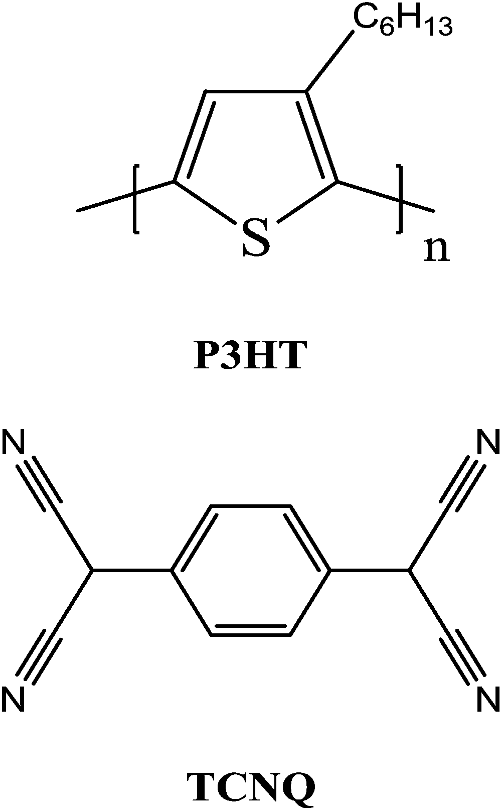 | ||
| Scheme 1 Chemical structure of P3HT and TCNQ. | ||
Results and discussion
We first varied the mass ratio of P3HT and TCNQ in chlorobenzene solution to investigate the hybrid performance (from 10![[thin space (1/6-em)]](https://www.rsc.org/images/entities/char_2009.gif) :1, 5:1, 1:1 to 1:10 mass ratio). The UV-vis absorption bands of P3HT and TCNQ revealed that there are some small changes in the mixture system around 400 nm band (Fig. 1), which might be due to the charge-transfer (CT) interaction between P3HT and TCNQ. To study the charge-transfer properties for P3HT/TCNQ hybrid system, we also investigated the photoluminescent (PL) behaviors of our mixed system. The emission spectra of P3HT, TCNQ and P3HT/TCNQ complex in chlorobenzene with different mass ratio are shown in Fig. S1.† The emission spectrum of TCNQ displays two peaks (438 nm and 460 nm), while the intensity of the two peaks decreased suddenly with P3HT adding, which may be owing to the charge transfer between P3HT and TCNQ. For the closed energy level of the selected typical donor polymer and acceptor, highest occupied molecular orbital (HOMO) of P3HT (−5.1 eV) and lowest unoccupied molecular orbital (LUMO) of TCNQ (−4.6 eV), the charge transfer and π–π interaction between them induced two different materials to self-assemble into a hybrid microstructure. A drop-casting method was employed for the preparation of microstructures of P3HT/TCNQ hybrid, which is a simple and effective technique to produce high-quality co-crystals of donor–acceptor complex. P3HT and TCNQ, mixed in chlorobenzene solution with a concentration of 1 mg ml−1, were poured onto the pre-cleaned substrates to grow wires. As shown in Fig. 2, P3HT/TCNQ hybrid microwires with a width from hundreds of nanometers to micrometers and a length from several millimeters to centimeters were obtained by evaporating mixed solution on distinct substrates (OTS/SiO2/Si, SiO2/Si and glasses. For details, see the Experimental section). The as-formed morphology was totally different from single component processed through the same method (P3HT: film, TCNQ: microplate, Fig. S2†). From the optical images, when P3HT was the main component (10:1 or 5:1), a series of the heterojunction-wire-aligned architectures have been fabricated. We supposed that in the evaporation step, small proportion of TCNQ molecules with good crystallinity induced polymer molecules to assemble into 1D structure. And also, more rigidity of small molecule would form well-ordered wires. With the decrease of polymer content, especially in a 1:1 ratio, wires tend to gather and form confluent plate-like architectures. When TCNQ became the major part, wires (or ribbons) with larger width and smaller length are observed, indicating that polymer chains are induced to grow along the long direction in this mixed system (Fig. S3†).
:1, 5:1, 1:1 to 1:10 mass ratio). The UV-vis absorption bands of P3HT and TCNQ revealed that there are some small changes in the mixture system around 400 nm band (Fig. 1), which might be due to the charge-transfer (CT) interaction between P3HT and TCNQ. To study the charge-transfer properties for P3HT/TCNQ hybrid system, we also investigated the photoluminescent (PL) behaviors of our mixed system. The emission spectra of P3HT, TCNQ and P3HT/TCNQ complex in chlorobenzene with different mass ratio are shown in Fig. S1.† The emission spectrum of TCNQ displays two peaks (438 nm and 460 nm), while the intensity of the two peaks decreased suddenly with P3HT adding, which may be owing to the charge transfer between P3HT and TCNQ. For the closed energy level of the selected typical donor polymer and acceptor, highest occupied molecular orbital (HOMO) of P3HT (−5.1 eV) and lowest unoccupied molecular orbital (LUMO) of TCNQ (−4.6 eV), the charge transfer and π–π interaction between them induced two different materials to self-assemble into a hybrid microstructure. A drop-casting method was employed for the preparation of microstructures of P3HT/TCNQ hybrid, which is a simple and effective technique to produce high-quality co-crystals of donor–acceptor complex. P3HT and TCNQ, mixed in chlorobenzene solution with a concentration of 1 mg ml−1, were poured onto the pre-cleaned substrates to grow wires. As shown in Fig. 2, P3HT/TCNQ hybrid microwires with a width from hundreds of nanometers to micrometers and a length from several millimeters to centimeters were obtained by evaporating mixed solution on distinct substrates (OTS/SiO2/Si, SiO2/Si and glasses. For details, see the Experimental section). The as-formed morphology was totally different from single component processed through the same method (P3HT: film, TCNQ: microplate, Fig. S2†). From the optical images, when P3HT was the main component (10:1 or 5:1), a series of the heterojunction-wire-aligned architectures have been fabricated. We supposed that in the evaporation step, small proportion of TCNQ molecules with good crystallinity induced polymer molecules to assemble into 1D structure. And also, more rigidity of small molecule would form well-ordered wires. With the decrease of polymer content, especially in a 1:1 ratio, wires tend to gather and form confluent plate-like architectures. When TCNQ became the major part, wires (or ribbons) with larger width and smaller length are observed, indicating that polymer chains are induced to grow along the long direction in this mixed system (Fig. S3†).
 | ||
| Fig. 1 Absorption spectra of P3HT, TCNQ and P3HT/TCNQ complex in chlorobenzene with different mass ratio. The inset image shows the detailed absorption near 400 nm. | ||
 | ||
| Fig. 2 Optical images of P3HT/TCNQ hybrid microstructures obtained by the drop-casting method with different mass ratios: 10:1 (a), 5:1 (b), 1:1 (c), 1:10 (d). | ||
In addition, atomic force microscopy (AFM) is also employed to characterize the structures and morphologies of the as-fabricated hybrids. Fig. 3a showed the image of one single wire of the as-prepared hybrid structure with the width about 1 μm. Absorption spectra of P3HT/TCNQ hybrid microstructures on glass were presented in Fig. 3b.
 | ||
| Fig. 3 (a) AFM image of P3HT/TCNQ hybrid microstructure, (b) absorption spectra of P3HT/TCNQ hybrid microstructures on glass. | ||
The powder X-ray diffraction was conducted to investigate the possible structures of the as-prepared hybrid microwires (as shown in Fig. S4†). In 10:1, 5:1 and 1:1 ratio systems, no apparent peaks were observed (only the background), which might imply that in these hybrid microstructures, the molecules did not grow into a well-ordered packing structure; while a sharp diffractive peak at 2theta = 27.1° could be seen in 1:10 system (corresponding to a π–π distance of 3.3 Å), which might attribute to better crystallinity resulted from major small molecules.
To investigate the influence of microstructures on transport, we manufactured transistor devices through thermally evaporating Au source/drain electrodes onto the long wires/plates via a copper grid mask method. An individual copper grid with arm length about 20 μm as a mask was picked up by a mechanical tweezer and crossed over the as-prepared P3HT/TCNQ hybrid structures. Subsequently, source/drain electrodes were vacuum-deposited on the structure, and finally, the copper grid was peeled off by the tweezers and one microstructure transistor with the expected length of 20 μm was fabricated.
Fig. 4a and b show a schematic representation and an optical microscopy image of hybrid microstructure transistor, respectively. Typically, the measured transfer and output characteristics of the 10:1 wire-aligned architecture-based device are shown in Fig. 4c and d. From the transfer characteristics, the best hole field-effect mobility (μ) was calculated to be 0.09 cm2 V−1 s−1 with the mass ratio of 10:1 under ambient conditions. Compared to the transport properties of P3HT thin film transistors (0.04 cm2 V−1 s−1), the hole mobility of this micro/nanowire appeared to be doubled. Although no apparent evidence to imply good packing mode in this polymer/small molecule system was found, there was still effective transport channel in the long assembled microwires.
 | ||
| Fig. 4 (a) Schematic diagram and (b) optical image of the device with hybrid aligned microstructures. (c) Transfer and (d) output characteristics of the device with 10:1 ratio P3HT/TCNQ hybrid microwires. | ||
The as-fabricated microstructures showed obvious distinguishable transport properties according to the mass ratios. At 5:1 ratio, the mobility decreased a little bit (about 0.07 cm2 V−1 s−1) (Fig. 5a and b). While in 1:1, FETs based on wire-gathered plate exhibited ambipolar transport property. The obvious V-shape transfer curves with one arm indicating electron transporting (n-type) and the other suggesting hole transporting (p-type) were observed. The saturated electron and hole mobility could be extracted from the transfer curves. The electron and hole mobilities of 1:1 P3HT/TCNQ hybrid characterized from Fig. 5c and d are 5 × 10⁻⁵ and 5.3 × 10⁻⁶ cm2 V−1 s−1, respectively. Output characteristics of the transistors are presented in Fig. S4.† As to the 1:10 ratio where TCNQ is the major component, no obvious charge transport property (either hole or electron) were observed. In addition, the device fabrication and measurement have been repeated several times and all data are repeatable. These results suggested that when polymer was the main component, only hole transport through the hybrid microstructure existed; and, if the mixed mass ratio of P3HT and TCNQ was about 1:1, both hole and electron could transport; and when TCNQ became the primary part, no effective transport in the hybrid would happen. It can be concluded that the formation process of hybrid materials would induce a variation in the morphology of as-fabricated hybrid structures and further change their electrical transport properties. This factor would offer us a new strategy for adjusting the performance of polymer semiconductors.
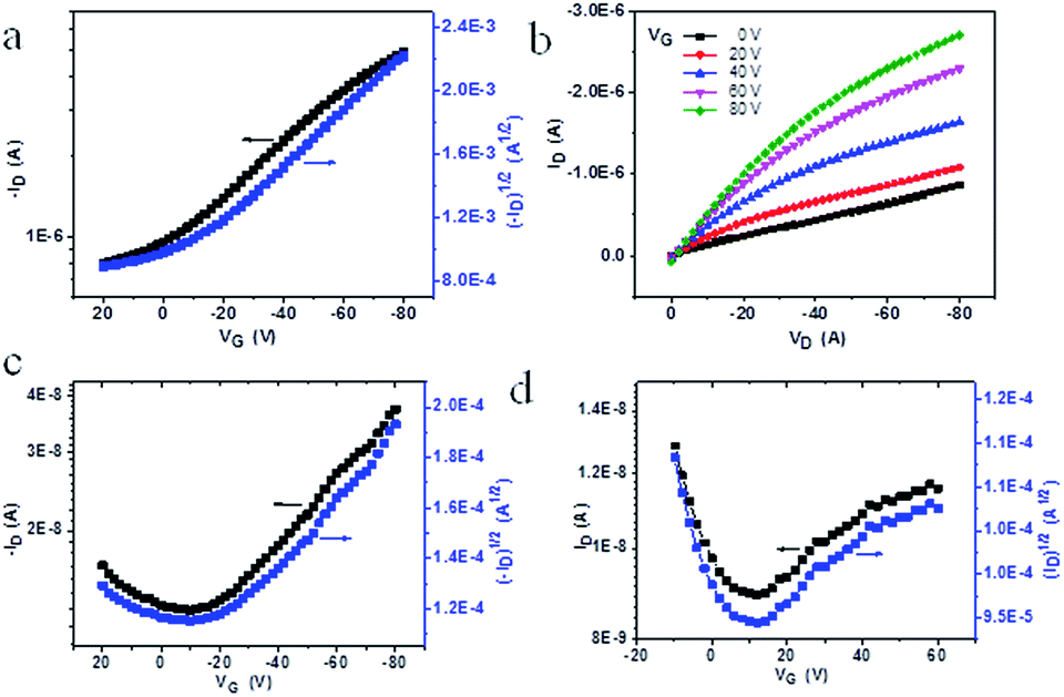 | ||
| Fig. 5 (a) Transfer and (b) output characteristics of the hybrid microstructure device with 5:1 ratio. (c) and (d) Transfer characteristics of the 1:1 P3HT/TCNQ hybrid based device. | ||
Conclusions
Attributed to the emerged charge transfer and π–π interaction, long hybrid P3HT/TCNQ microwires have been fabricated through simple solution-evaporation method. The FET performance of these as-prepared microstructures displayed p-type (10:1 and 5:1), ambipolar (1:1) or no charge carrier transport behaviours (1:10). Our research makes us believe that if the appropriate materials (polymer and small molecule) and their ratios were judiciously selected, hybrid architectures with excellent ferroelectrics, photoconductivity, and charge transport properties could be achieved. This research direction is still on the way.
Experimental
Materials
Poly(3-hexylthiophene) was were purchased from Aldrich Chemical Company and used without further purification. TCNQ was purchased from Aldrich Chemical Company and purified by gradient sublimation once before use.Growth of micro/nanowires and device fabrication
The SiO2/Si substrate was heavily doped n-type Si wafer with a 500 nm thick SiO2 layer and a capacitance of 7.5 nF cm−2. Bare substrates and glasses were successively cleaned with pure water, piranha solution (H2SO4:H2O2 = 2:1), pure water and pure isopropanol. Treatment of Si/SiO2 wafer with OTS used in the present study was carried out by vapour-deposition method. The clean wafers were dried under vacuum at 90 °C for 0.5 h in order to eliminate the influence of the moisture. After cooling to room temperature, a little drop of OTS was placed on the wafers. Subsequently, this system was heated to 120 °C and maintained for 2 h under vacuum. Then, the surface was modified with n-octadecyltrichlorosilane (OTS). After that, the substrates were cleaned in n-hexane, CHCl3 and pure isopropanol. The glasses were successively cleaned with pure water, acetone, CHCl3 and pure isopropanol. Hybrid microstructures of the donor–acceptor complex were conducted by using the drop-casting method. A chlorobenzene solution containing P3HT and TCNQ (1–2 mg ml−1, mass ratio 10:1, 5:1, 1:1 or 1:10) was poured over the substrates and the solvent evaporated at room temperature. Drain and source Au electrodes (40 nm thick) were deposited on the hybrid wires by thermal evaporation with a copper grid as the shadow mask.
Measurements
UV/Vis spectra were taken on a Hitachi 2501 PC spectrometer. AFM images were obtained with AFM Cypher S. X-ray diffraction (XRD) was measured on D8/max2500 with CuKα source (κ = 1.541 Å). I–V characteristics of the OFETs were recorded with a Keithley 4200 SCS and a Micromanipulator 6150 probe station in a clean and shielded box at room temperature in air.Acknowledgements
Q.Z. acknowledges financial support from AcRF Tier 1 (RG 16/12) and Tier 2 (ARC 20/12 and ARC 2/13) from MOE, and the CREATE program (Nanomaterials for Energy and Water Management) from NRF, Singapore.References
- (a) N. Robertson and C. A. McGowan, Chem. Soc. Rev., 2003, 32, 96–103 RSC; (b) K. S. Park, B. Cho, J. Baek, J. K. Hwang, H. Lee and M. M. Sung, Adv. Funct. Mater., 2013, 23, 4776–4784 CAS.
- (a) L. Zang, Y. K. Che and J. S. Moore, Acc. Chem. Res., 2008, 41, 1596–1608 CrossRef CAS PubMed; (b) A. L. Briseno1, S. C. B. Mannsfeld, S. A. Jenekhe, Z. Bao and Y. Xia, Mater. Today, 2008, 11, 38–47 CrossRef.
- (a) S. Y. Min, T. S. Kim, B. J. Kim, H. Cho, Y. Y. Noh, H. Yang, J. H. Cho and T. W. Lee, Nat. Commun., 2013, 4, 1773, DOI:10.1038/ncomms2785; (b) Y. W. Lin, C. J. Lin, Y. H. Chou, C. L. Liu, H. C. Chang and W. C. Chen, J. Mater. Chem. C, 2013, 1, 5336–5343 RSC.
- (a) Q. H. Cui, Y. S. Zhao and J. N. Yao, J. Mater. Chem., 2012, 22, 4136–4140 RSC; (b) C. Zhang, Y. Yan, Y. S. Zhao and J. Yao, Annu. Rep. Prog. Chem., Sect. C: Phys. Chem., 2013, 109, 211–239 RSC.
- (a) S. Cui, H. Liu, L. Gan, Y. Li and D. Zhu, Adv. Mater., 2008, 20, 2918–2925 CrossRef CAS; (b) C. M. Hangarter, M. Bangar, A. Mulchandani and N. V. Myung, J. Mater. Chem., 2010, 20, 3131–3140 RSC.
- (a) J. H. Oh, H. W. Lee, S. Mannsfeld, R. M. Stoltenberg, E. Jung, Y. W. Jin, J. M. Kim, J. B. Yoo and Z. N. Bao, Proc. Natl. Acad. Sci. U. S. A., 2009, 106, 6065–6070 CrossRef CAS PubMed; (b) Z. Wang, R. Bao, X. Zhang, X. Ou, C.-S. Lee, J. C. Chang and X. Zhang, Angew. Chem., Int. Ed., 2011, 50, 2811–2815 CrossRef CAS PubMed.
- (a) C. Giansante, G. Raffy, C. Schäfer, H. Rahma, M. T. Kao, A. G. L. Olive and A. D. Guerzo, J. Am. Chem. Soc., 2011, 133, 316–325 CrossRef CAS PubMed; (b) J. Xiao, Z. Yin, H. Li, Q. Zhang, F. Boey, H. Zhang and Q. C. Zhang, J. Am. Chem. Soc., 2010, 132, 6926–6928 CrossRef CAS PubMed; (c) J. Xiao, B. Yang, J. I. Wong, Y. Liu, F. Wei, K. J. Tan, X. Teng, Y. Wu, L. Huang, C. Kloc, F. Boey, J. Ma, H. Zhang, H. Yang and Q. Zhang, Org. Lett., 2011, 13, 3004–3007 CrossRef CAS PubMed; (d) J. Xiao, Z. Yin, Y. Wu, J. Guo, Y. Cheng, H. Li, Y. Z. Huang, Q. Zhang, J. Ma, F. Boey, H. Zhang and Q. Zhang, Small, 2011, 7, 1242–1246 CrossRef CAS PubMed.
- (a) D. Kluge, J. C. Singer, J. W. Neubauer, F. Abraham, H. W. Schmidt and A. Fery, Small, 2012, 8, 2563–2570 CrossRef CAS PubMed; (b) Y. Liu, F. Boey, L. L. Lao, H. Zhang, X. Liu and Q. Zhang, Chem.–Asian J., 2011, 6, 1004–1006 CrossRef CAS PubMed; (c) J. Xiao, D. Y. Kusuma, Y. Wu, F. Boey, H. Zhang, P. See Lee and Q. Zhang, Chem.–Asian J., 2011, 6, 801–803 CrossRef CAS PubMed.
- (a) L. Jiang, Y. Y. Fu, H. X. Li and W. P. Hu, J. Am. Chem. Soc., 2008, 130, 3937–3941 CrossRef CAS PubMed; (b) J. Xiao, H. Yang, Z. Yin, J. Guo, F. Boey, H. Zhang and Q. Zhang, J. Mater. Chem., 2011, 21, 1423–1427 RSC; (c) J. Xiao, Z. Yin, B. Yang, Y. Liu, L. Ji, J. Guo, L. Huang, X. Liu, Q. Yan, H. Zhang and Q. Zhang, Nanoscale, 2011, 3, 4720–4723 RSC.
- Y. Hizume, K. Tashiro, R. Charvet, Y. Yamamoto, A. Saeki, S. Seki and T. Aida, J. Am. Chem. Soc., 2010, 132, 6628–6629 CrossRef CAS PubMed.
- Y. B. Guo, L. Xu, H. B. Liu, Y. J. Li, C. M. Che and Y. L. Li, Adv. Mater., 2015, 27, 985–1013 CrossRef CAS PubMed.
- (a) K. S. Park, S. M. Salunkhe, I. Lim, C. G. Cho, S. H. Han and M. M. Sung, Adv. Mater., 2013, 25, 3351–3356 CrossRef CAS PubMed; (b) B. Yang, J. Xiao, J. I. Wong, J. Guo, Y. Wu, L. Ong, L. L. Lao, F. Boey, H. Zhang, H. Yang and Q. Zhang, J. Phys. Chem. C, 2011, 115, 7924–7927 CrossRef CAS; (c) J. Zhao, J. I. Wong, C. Wang, J. Gao, V. Z. Y. Ng, H. Y. Yang, S. C. J. Loo and Q. Zhang, Chem.–Asian J., 2013, 8, 665–669 CrossRef CAS PubMed.
- Y. Liu, H. L. Dong, S. D. Jiang, G. Y. Zhao, Q. Q. Shi, J. H. Tan, L. Jiang, W. P. Hu and X. W. Zhan, Chem. Mater., 2013, 25, 2649–2655 CrossRef CAS.
- T. Lei, Z. H. Guo, C. Zheng, Y. Cao, D. H. Liang and J. Pei, Chem. Sci., 2012, 3, 1162–1168 RSC.
- T. Lei, Y. Cao, Y. L. Fan, C. J. Liu, S. C. Yuan and J. Pei, J. Am. Chem. Soc., 2011, 133, 6099–6101 CrossRef CAS PubMed.
- X. Zhan, Z. Tan, B. Domercq, Z. An, X. Zhang, S. Barlow, Y. Li, D. Zhu, B. Kippelen and S. R. Marder, J. Am. Chem. Soc., 2007, 129, 7246 CrossRef CAS PubMed.
- H. Yan, Z. H. Chen, Y. Zheng, C. Newman, J. R. Quinn, F. Dotz, M. Kastler and A. Facchetti, Nature, 2009, 457, 679 CrossRef CAS PubMed.
- H. J. Chen, Y. L. Guo, G. Yu, Y. Zhao, J. Zhang, D. Gao, H. T. Liu and Y. Q. Liu, Adv. Mater., 2012, 24, 4618–4622 CrossRef CAS PubMed.
- J. Li, Y. Zhao, H. S. Tan, Y. L. Guo, C. A. Di, G. Yu, Y. Q. Liu, M. Lin, S. H. Lim, Y. H. Zhou, H. B. Su and B. S. Ong, Sci. Rep., 2012, 2, 754 Search PubMed.
- J. H. Kim, D. H. Lee, D. S. Yang, D. U. Heo, K. H. Kim, J. Shin, H. J. Kim, K. Y. Baek, K. Lee, H. Baik, M. J. Cho and D. H. Choi, Adv. Mater., 2013, 25, 4102–4106 CrossRef CAS PubMed.
- Y. Liu, H. F. Wang, H. L. Dong, L. Jiang, W. P. Hu and X. W. Zhan, small, 2013, 9, 294–299 CrossRef CAS PubMed.
- (a) H. L. Dong, S. D. Jiang, L. Jiang, Y. L. Liu, H. X. Li, W. P. Hu, E. J. Wang, S. K. Yan, Z. M. Wei, W. Xu and X. Gong, J. Am. Chem. Soc., 2009, 131, 17315–17320 CrossRef CAS PubMed; (b) J. Wu, Y. Sun, W. Xu and Q. Zhang, Synth. Met., 2014, 189, 177–182 CrossRef CAS PubMed; (c) J. Wu, Y. Sun, W.-B. Pei, L. Huang, W. Xu and Q. Zhang, Synth. Met., 2014, 196, 173–177 CrossRef CAS PubMed.
- K. P. Goetz, D. Vermeulen, M. E. Payne, C. Kloc, L. E. McNeil and O. D. Jurchescu, J. Mater. Chem. C, 2014, 2, 3065–3076 RSC.
- L. Zhu, Y. Yi, Y. Li, E.-G. Kim, V. Coropceanu and J. Bredas, J. Am. Chem. Soc., 2012, 134, 2340–2347 CrossRef CAS PubMed.
- J. Zhang, H. Geng, T. S. Virk, Y. Zhao, J. Tan, C. Di, W. Xu, K. Singh, W. Hu, Z. Shuai, Y. Liu and D. Zhu, Adv. Mater., 2012, 24, 2603–2607 CrossRef CAS PubMed.
- J. Zhang, J. Tan, Z. Ma, W. Xu, G. Zhao, H. Geng, C. Di, W. Hu, Z. Shuai, K. Singh and D. Zhu, J. Am. Chem. Soc., 2013, 135, 558–561 CrossRef CAS PubMed.
- C. J. Brabec, S. Gowrisanker, J. J. M. Halls, D. Laird, S. J. Jia and S. P. Williams, Adv. Mater., 2010, 22, 3839–3856 CrossRef CAS PubMed.
- R. J. Kline, M. D. McGehee, E. N. Kadnikova, J. S. Liu, J. M. J. Frechet and M. F. Toney, Macromolecules, 2005, 38, 3312–3319 CrossRef CAS.
- E. Menard, V. Podzorov, S.-H. Hur, A. Gaur, M. E. Gershenson and J. A. Rogers, Adv. Mater., 2004, 16, 2097–2101 CrossRef CAS.
Footnote |
| † Electronic supplementary information (ESI) available. See DOI: 10.1039/c5ra01167a |
| This journal is © The Royal Society of Chemistry 2015 |