DOI:
10.1039/C5RA01152C
(Paper)
RSC Adv., 2015,
5, 23101-23113
Structural interpretation, growth mechanism and optical properties of ZnO nanorods synthesized by a simple wet chemical route†
Received
20th January 2015
, Accepted 13th February 2015
First published on 16th February 2015
Abstract
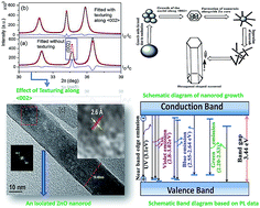
ZnO nanorods are synthesized at room temperature through a simple chemical process without using any template or capping agent. ZnO nanopowders used in this synthesis are synthesized by mechanically alloying the ZnO powder. Here, we report primarily the crystal structure and microstructure interpretations of ZnO nanorods by analyzing X-ray diffraction patterns employing Rietveld refinement, field emission scanning electron microscopy (FESEM) and high resolution transmission electron microscopy (HRTEM) with energy dispersive X-ray (EDX) spectroscopy techniques. Uniformly shaped pure ZnO nanorods with different lengths and diameters are synthesized within 5 h of reaction time. The Rietveld refinement and HRTEM images ascertain the growth of ZnO nanorods along the <002> plane. STEM-HAADF images and EDX spectra and imaging of nanorods confirm the chemical composition and reveal the uniform elemental distributions of Zn and O over the entire nanorod. UV-visible spectra analyses of ZnO nanopowder and nanorods reveal a small decrease in optical band gap of nanorods due to morphological change. Photoluminescence (PL) spectra of both powder and rod-shaped ZnO reveal the presence of excess of oxygen in nanorods. Rietveld analysis corroborates the findings of PL and quantifies the content of oxygen in ZnO nanorods.
1. Introduction
Control over different morphologies and the detailed analysis of the crystal structure and microstructure of nanomaterials are two important and useful aspects to maneuver their properties. One dimensional semiconductor nanocrystals, especially transition metal oxide semiconductors such as ZnO, TiO2, CuO, NiO, and FeO, have attracted considerable attention due to their exclusive optical and electrical properties, and they have become the potential candidates in modern electronic and photonic devices. Among them, ZnO has become the promising functional material because it possesses a wide band gap (n type, Eg = 3.37 eV) with wurtzite structure and large exciton binding energy (60 meV) at room temperature with good chemical and thermal stabilities, and outstanding electrochemical properties due to high surface to volume ratio.1,2 Considerable effort has been dedicated for the preparation of various one dimensional ZnO nanostructures, such as nanorods, nanowires, nanotubes, nanoneedles, nanobelts, and nanopillars,3–6 because of their nontoxic nature and unique electrical, semiconducting and piezoelectric properties.7,8 In particular, these one dimensional structures of ZnO exhibit excellent performance in various devices and are suitable in a broad range of modern technological applications such as surface acoustic wave filters,9 piezo nanogenerators,10,11 photonic devices,12 light emitting diodes,13 photodetectors,14 gas sensors,15 lithium ion batteries,16 photocatalytic activity17 and solar cells.18
In literature, various synthesis techniques have been reported for the preparation of uniform sized ZnO nanorods, and they can be classified in two categories: (i) chemical vapour deposition,19,20 which is a high temperature synthesis, generally involving temperatures above 550 °C and (ii) soft chemical synthesis, generally involving temperatures below 200 °C (ref. 21) such as hydrothermal/solvothermal synthesis,22,23 template assisted method,24 vapor–liquid–solid method (VLS),25 electrochemical deposition26,27 and sol–gel method.28 Here, we adopt a simple chemical route29 by which uniform ZnO nanorods a few micrometers long with ∼20 nm uniform diameter can be grown without using any template or capping agent at room temperature. This simple process can also be extended to synthesize other metal oxides. Pacholski et al.30 reported that anisotropic crystal growth associated with the oriented attachment of preformed quasi-spherical ZnO nanoparticles was the major reason for the single crystalline nanorod formation because the free surface energy of various crystallographic planes differ significantly and ZnO nanorods were grown along the c axis (002) of the hexagonal wurtzite lattice of ZnO. Feng et al.31 reported the wettability of aligned ZnO nanorods grown along the <001> plane, and this anisotropic growth of nanorods was associated with the lower velocity of crystal growth along the <002> plane, which led to the slower growth of (002) planes with lower surface energy. ZnO nanorods had been synthesized by different chemical routes; however, in most of the earlier cases, their detailed structural characterization and interpretation were not revealed satisfactorily.17,29,32–34
Our primary objective is to characterize ZnO nanorods in terms of structural and microstructural parameters for better understanding of their growth mechanism. However, due to the morphological complexity, structure interpretation of these nanomaterials needs some special considerations, e.g. the basis of preferential growth mechanism in a particular direction. X-ray diffraction (XRD) technique can overcome the different structural complexity in these materials, which arises from various morphological aspects. Rietveld refinement method35–37 enables the quantification of different structure micro/nano structure parameters, such as lattice parameters, atomic coordinates and occupancies, crystallite size, and lattice strain, of this type of material to a good degree of precision using the readily available XRD data.38
The Rietveld structure refinement method can precisely measure both structure and microstructure parameters of any polycrystalline material. However, if a polycrystalline material grows along a particular direction then texturing/preferred orientation effect on the growth of crystal lattice should be included in the Rietveld analysis. In the case of ZnO nanopowder, no texturing effect is present; however, ZnO nanorods are grown along the <002> plane. It is therefore very important to carry out quantitative texture analysis (QTA) of XRD patterns for proper interpretations in terms of structure and microstructure analysis.39 In the present study, the March–Dollase equation40 has been adopted due to the fact that it can measure the crystallographic texture with the preferred orientation of crystal lattice within the material.
Hu et al.41 fabricated shuttle shaped Mn2O3/ZnO nanocomposites and studied their optical properties by UV-Vis and PL spectroscopy measurements. In their PL spectra, they observed a strong UV light emission peak at 367 nm corresponding to transition band gap energy of 3.38 eV. A considerable blue shift was also observed with respect to the edge emission gap energy of bulk ZnO nanocrystals due to quantum confinement effect.
Optical properties of both powder and rod-shaped ZnO nanocrystals have been studied in detail through UV-visible absorption and photoluminescence (PL) spectroscopies. In the present work, our main objectives are to (i) synthesize nanocrystalline ZnO powder and rods through physical and chemical processes, (ii) study the formation mechanism of ZnO nanorods from the crystal structure and microstructure points of view employing both the Rietveld refinement and HRTEM image analyses, and (iii) reveal the change in optical band gap due to morphological change and explain the origin of different PL emission peaks both in ZnO nanopowder and nanorods in detail.
2. Experimental
2.1. Synthesis of ZnO nanorod
Zn metal powder (99%, Sigma Aldrich), sodium hydroxide (NaOH) pellets (97%, Merck) and ammonium peroxodisulphate (NH4)2S2O8 (98%, Merck) were taken as precursors. For the synthesis of ZnO nanorods, two solutions were prepared separately by dissolving 0.038 mol of ammonium peroxodisulphate and 0.191 mol of sodium hydroxide each in 20 ml deionized water at ambient temperature, and 0.9 g Zn metal powder was dissolved in 10 ml of deionized water. With continuous stirring of Zn powder solution, a mixture of the other two solutions was added dropwise, and the stirring was continued up to 30 min, 1 h, 3 h, 5 h, 6 h, 10 h and 20 h durations. Finally, the white precipitate was collected after each time interval and washed thoroughly in deionized water and ethanol repeatedly and dried at room temperature.29
The nanocrystalline ZnO powder was synthesized by mechanically alloying the commercial grade ZnO (E Merck, purity > 99%) precursors. Milling of the polycrystalline ZnO powder was performed in a high-energy planetary ball mill (Model: P5, M/s FRITSCH, GmbH, Germany) in air medium at room temperature in a chrome steel vial; 80 ml of its volume was filled with chrome steel balls having a diameter of 10 mm.
2.2. Material characterization
The surface morphology of the ZnO nanorods was examined through a field emission scanning electron microscope (FESEM). The crystallinity and the phase purity of the samples were inspected from X-ray powder diffraction (XRD) patterns, which were recorded by employing Ni filtered CuKα radiation from a Rigaku TTRAX II diffractometer. The operating voltage and tube current during XRD measurements were 60 kV and 150 mA, respectively. Step scan data with step size of 2θ = 0.02° and time per step 5–10 s (depending upon relative peak intensity) within the annular range of 2θ = 20–80° were recorded. The detailed structural analysis of ZnO nanorods was performed using a high resolution transmission electron microscope (HRTEM) (FEI, TF30, ST) operated at 300 kV. The TF30 microscope is equipped with a high-angle annular dark field (HAADF) detector (Fischione, Model: 3000) and a scanning unit. Energy-filtered TEM (EFTEM) measurements were carried out using a post column imaging filter (Quantum SE, Model: 963) from GATAN Inc. The optical absorbance spectra of both powder and rod-like ZnO samples were measured in a UV-Vis spectrophotometer (SHIMA-DZU UV-1800, JAPAN). The emission spectra of the samples were recorded using a fluoro Max-P (Horiba Jobin-Yvon) luminescence spectrometer, and the measurements were performed at room temperature using a solid sample holder. The excitation wavelength of ZnO nanopowder was 330 nm and that of ZnO nanorod was 365 nm.
2.3. Method of analysis
The Rietveld powder structure refinement method42 using X-ray powder diffraction data is one of the best methods for obtaining several structural parameters such as atomic coordinates, occupancies, lattice parameters and thermal parameters, micro/nano structural parameters, like particle size and r.m.s., and lattice strain as well as for the quantitative phase estimation of a multiphase material. In the present work, we have adopted this method to obtain structure and micro/nano structural parameters of ZnO nanopowder and nanorod samples prepared with different reaction/stirring times. The Rietveld software MAUD 2.26 (ref. 43) is specially designed to simultaneously refine both structural and microstructural parameters through Marquardt least-squares method. Because the peaks are significantly broadened with asymmetry, the shape of the diffraction profiles is modeled with a pseudo-Voigt (pV) function with asymmetry as it takes care of both the particle size and strain broadening of the experimental profiles individually. To fit the experimental profiles of the samples taking into account all types of instrumental corrections, we have modeled the simulated patterns by refining some important structural and microstructural parameters such as particle (coherently diffracting domain) sizes and r.m.s. lattice strain. XRD patterns are simulated considering the respective phases of metallic Zn and ZnO in a single diffraction pattern. It may be noted that the Caglioti parameters, namely, U, V and W (Caglioti et al. 1958),44 instrumental asymmetry and Gaussianity parameters were obtained for the instrumental setup (instrumental corrections) using a Si standard and kept unchanged during refinements. The background of each pattern is fitted by a polynomial of degree 5. Positions of all the peaks are fitted through the successive refinements of zero shift error. Assuming the integrated intensity as a function of structural and microstructural parameters, Marquardt least-squares procedure is adopted for the minimization of the difference between the observed and simulated powder diffraction patterns, and the minimization is monitored using the reliability index parameter, Rwp (weighted residual error) and Rexp (expected error) defined respectively as follows:
where IO and IC are the experimental and calculated intensities, wi (=1/IO) and N are the weight and number of experimental observations respectively, and P represents the number of fitting parameters. This leads to the value of goodness of fit (GoF):
GoF values in all the cases remain very close to 1.0. The relative X-ray intensity of the (002) reflection of the ZnO nanorod is significantly high (I002
:
I101 = 0.86) in comparison to the ZnO powder (ICSD database no. 65121) (I002
:
I101 = 0.44). This indicates that ZnO nanorods are grown preferably along the <002> plane. To account for the crystal orientation effect, we adopt the March–Dollase equation as the model to fit the texture distribution along the direction of growth of nanorods. The March equation was first introduced to determine the preferred orientation of anisotropic particles.40 Dollase later modified the March equation to fit the preferred orientation in the Rietveld analysis, and the modified March–Dollase equation is as follows:
where
Thkl is the preferred orientation factor,
τ is the preferred orientation parameter, which is refinable in Rietveld analysis,
ϕ is the angle between the preferred orientation vector and the normal to the planes generating the diffracted peak,
N is the symmetrically equivalent reciprocal lattice points. In the present study, we have determined the preferred orientation and texture parameters of the rod-shaped ZnO using this March–Dollase equation with the help of Rietveld software MAUD 2.26.
43
2.3.1. Proposed growth mechanism of ZnO nanorods. To obtain a detailed understanding about the formation of ZnO nanorods, a possible growth mechanism has been proposed here.29,45 It is well known from the classical nucleation theory that in a solution based process, supersaturation is the basic requirement for both nucleation and growth. The energy barrier for nucleation may be overcome through the following steps: (i) either by performing the reaction at room temperature or (ii) by increasing the level of supersaturation or both. In our case, an aqueous solution of Zn metal powder is mixed with NaOH solution and in this highly alkaline environment, Zn metal powder solution continuously releases Zn2+ ion in the form of Zn(OH)42− (zincate ions) following the dissolution reaction,
Zn + 4NaOH → Zn(OH)42− + 4Na+ |
Finally, in this solution, Zn(OH)42− concentration (i.e. Zn2+ ions) increases with the reaction time due to the continuous release of zinc ions into the solution through the formation of Zn(OH)2. This is directly confirmed from the XRD patterns, as shown in Fig. 1. Therefore, for this increase in Zn(OH)42− concentration, a suitable saturation level has been obtained, which is sufficient to overcome the nucleation energy barrier. Finally, the oxidation of zincate ions occurs in two steps by the addition of ammonium peroxodisulphate through the following oxidative reactions:
 |
| Fig. 1 XRD patterns of the samples obtained at the initial stage of reaction before complete formation. | |
Step 1: (up to 3 h of reaction time)
Zn(OH)42− + Na+ + (NH4)2S2O8 → Zn(OH)2 + (NH4)2SO4 + NH3↑ + Na2SO4 |
Step 2: (at and after 5 h of reaction time)
Thus, the formation of heterogeneous nuclei of zinc oxide over zinc core occurs through this oxidation process. Furthermore, the continuous dissolution of zinc core occurs with the increase of reaction time. It is well known that wurtzite ZnO crystal can be described as a combination of a number of alternating planes composed of tetrahedrally coordinated O2− (00.
) and Zn2+ (00.1) ions stacked along the c-axis,46 which leads to a spontaneous polarization along the c-axis. The growth rate of the family of planes follows the sequence (00.1) > (
0.
) > (
0.1) > (00.
) for this polar crystal structure of ZnO.47 This concludes that one dimensional ZnO has a normal tendency to grow along the c-axis with (00.1) direction (similar to (002) direction) being the top surface and the non-polar surfaces as the side surfaces. This anisotropic growth behaviour leads to the growth of nanorods. Reaction for an optimum time of 5 h results in the complete dissolution of Zn(OH)2 and growth of isolated ZnO nanorods with uniform diameters. This complete growth mechanism has been schematically shown in the following diagram (Scheme 1).
 |
| Scheme 1 Schematic diagram of the formation mechanism of ZnO nanorod. | |
3. Results and discussions
3.1. Nanostructure characterization by XRD
3.1.1 Phase confirmation and phase content estimation. Fig. 2 represents the XRD patterns of ZnO nanorod synthesized through a simple chemical processing for different reaction times. It is clearly evident from the indexed pattern that after 5 h of stirring (reaction time) the complete formation of pure ZnO (ICSD database code 65121; Sp.Gr. P63mc; hexagonal; a = b = 3.25682 Å and c = 5.21251 Å) has been noticed through the step 2 reaction mechanism without any impurity from the precursor materials. It may be noted that except (002) reflection, all other reflections are relatively broadened, and some reflections are partially overlapped. After increasing the reaction time to 6 h, 10 h and 20 h there is no significant change noticed in the respective XRD patterns. The most interesting part of these patterns lies in the intensity of (002) reflection, which is stronger than that of the 2nd strongest reflection (100) of the polycrystalline ZnO nanopowder. The ideal intensity ratio of I002
:
I100 = 0.740 in ZnO powder becomes 1.389 in nanorods, indicating that these nanorods are extremely oriented along the <002> plane. From FESEM and HRTEM images, it has been found that after 5 h of stirring, ZnO nanorods of uniform diameter have been synthesized. Thus, this confirms that ZnO nanorods with preferential growth along the <002> plane have been obtained within 5 h of stirring of the precursors at ambient temperature. In previous works,29,30 the synthesis of ZnO nanorods was reported, but the degree of orientation of those nanorods along the <002> plane and the mechanism of the formation of nanorods were not explored in detail. One of the main objectives in the present study is to explore the structural morphology of ZnO nanorods with the help of the Rietveld structure/microstructure refinement method employing the March–Dollase function using XRD data in terms of the degree of preferred orientation and the role of oxygen occupancy in the growth of ZnO nanorods.
 |
| Fig. 2 Indexed XRD patterns of chemically synthesized ZnO nanorods obtained after different reaction times. | |
The Rietveld refinement method is a powerful and unique technique for determining the shape and size of the nanoparticles (coherently diffracting domain). Typical Rietveld analysis outputs of XRD patterns of ZnO nanopowder and nanorods are shown in Fig. 3(a) and (b), respectively. They clearly show that in the case of nanorod, peaks are less broadened and clearly resolved than those of the powder pattern. More clearly, it can be seen that peak-width of all the reflections obtained for the ZnO nanopowder, which was prepared by mechanical alloying, are almost equal; however, in the case of nanorods, the peak for (002) is less broadened in comparison to other reflections. This indicates that ZnO powder is composed of isotropic particles; however, in the case of nanorods, particles are anisotropic and elongated along the <002> plane. From the profile fitting residue (IO–IC), it is clear that the fitting quality of these patterns is considerably good. The structural and microstructural parameters of ZnO nanopowder and nanorods obtained from Rietveld analysis are shown in Table 1 and 2, respectively.
 |
| Fig. 3 Observed (red dotted pattern) X-ray diffraction pattern and corresponding Rietveld structure refinement output patterns (solid black pattern) of (a) particle and (b) rod-shaped ZnO nanomaterials. IO–IC represents the difference between the observed and calculated intensities of the XRD pattern. | |
Table 1 Structure and microstructural parameters obtained from the Rietveld analysis of ZnO nanopowder
Particle shape |
Lattice parameters (Å) |
Particle size (nm) |
Microstrain × 10−6 |
a |
c |
Spherical |
3.2467 |
5.20512 |
17.22 |
1.924 |
Table 2 Variation of structural parameters, content of ZnO and Zn in ZnO nanorods synthesized after different reaction time obtained from Rietveld analysis
Particle shape |
Stirring time (h) |
Lattice parameters (Å) |
Atomic coordinate |
Oxygen occupancy |
a |
c |
Rod |
5 |
3.2514 |
5.2074 |
0.376 |
1.070 |
6 |
3.2526 |
5.2090 |
0.371 |
1.103 |
10 |
3.2539 |
5.2090 |
0.373 |
1.089 |
20 |
3.2519 |
5.2069 |
0.369 |
1.137 |
The Rietveld analysis output patterns of ZnO nanorods formed by stirring the precursor solutions for different reaction times 5 h, 6 h, 10 h, and 20 h are shown in Fig. 4. The simulated XRD patterns of Rietveld analysis for the samples are analyzed with ZnO phase (ICSD database code 65121, hexagonal). All the experimental patterns are well fitted by refining the structural and microstructural parameters of the respective simulated patterns, as shown in the Fig. 4. Fitting qualities of all these experimental patterns are considerably good. The residual intensities (IO–IC) are plotted below the respective pattern, and peak positions of ZnO phase is indicated with markers (|). There is no trace of unreacted Zn in all the samples. The refined values of lattice parameters, which are tabulated in Table 2, are slightly less than that of the reported ICSD value. All the experimental patterns are well refined by considering the anisotropic nature of the particle size and lattice strain distributions of the line broadening model. The variations of particle size and lattice strains with different stirring time for different lattice planes in tabular form, as well as in graphical plots, are included in the ESI (See ESI, Table S1, Fig. S1 and S2†). The March–Dollase coefficients (degree of preferential orientation ranges from 1.0 to 0.0) obtained from Rietveld refinement along the <002> planes for all the patterns are in the range of 0.4–0.6 (with consideration, 1.0 → no/random orientation; 0.0 → perfect/full orientation) and tabulated in Table 2. This quantification of texturing suggests that a strong preferential growth is present in the stable rod shape of ZnO. A detailed structural analysis for the growth of rod-shaped ZnO has been discussed in the present study, which was not been done in earlier studies.29–32 In Table 2, variations of atomic coordinate and oxygen occupancy with reaction time are reported, and it can be seen that ZnO nanorods contain excess amounts (>1.0) of oxygen (adsorbed) in the lattice. It may be noted that there is an inverse relation between the increase of the displacement of oxygen atomic coordinate with the decrease of excess of oxygen content in ZnO lattice.
 |
| Fig. 4 Typical Rietveld analysis output patterns of ZnO nanorods obtained after different stirring/reaction times. | |
The upper part in Fig. 5 represents the XRD pattern of ZnO nanorod refined without considering oxygen occupancy factor in the Rietveld analysis. It can be clearly observed that there is a minor mismatch between the observed (red dotted line) and the calculated (solid black line) intensities of three major reflections, namely, (100), (002) and (101), and the profile fitting residues (IO–IC) are also poor for these reflections. Fitting residues have been reduced considerably after refining the oxygen occupancy in XRD pattern, as shown in the lower part of Fig. 5. The refined value of oxygen occupancy ranges from ∼1.07 to 1.13 (Table 2) (with the convention: occupancy = 1.0, no vacancy; <1.0, with vacancy and >1.0 contains excess oxygen). Thus, the Rietveld refinement reveals the presence of excess oxygen content in all the ZnO nanorods formed at different times of stirring/reaction. This finding is further confirmed from the analysis of PL spectra of these nanorods.
 |
| Fig. 5 Presence of excess oxygen in rod-like ZnO nanocrystals revealed from detailed Rietveld analysis. Solid black pattern represents the value of IO–IC. | |
3.2. Texturing effect of ZnO nanorod morphology
Fig. 6(a) depicts the XRD pattern of ZnO nanorods, which is refined without any texturing effect in the Rietveld analysis. It is evident from the analysis that there is a significant mismatch between the observed (red dotted line) and calculated (solid black line) intensity of (002) reflection, and from the profile residue IO–IC, it is clear that the profile fitting quality is reasonably poor particularly for this reflection. The additional intensity of the (002) reflection is computed to the preferential growth of nanorods along this direction. Considering this as the preferential growth direction, the XRD pattern is fitted by the Rietveld refinement employing the March–Dollase equation, and final fitted pattern is shown in Fig. 6(b). It is evident that the quality of fitting has been improved extensively, and there is no intensity mismatch along <002>. Thus, the preferential growth of ZnO nanorods along <002> has been established. Because the interplanar distance, d002 values, of ZnO and precursor Zn metal powder are 2.6046 Å and 2.473 Å, respectively, which are considerably close, the probability of the growth of ZnO nanorods along <002> is more than any other direction.
 |
| Fig. 6 Presence of texturing along <002> ZnO nanorods: (a) Rietveld refinement without texturing and (b) considering texturing effect. IO–IC represents the difference between the observed and calculated intensities of the respective XRD patterns. | |
Some agglomerated ZnO nanorods obtained after 6 h of reaction time are shown in Fig. 7(a) and (b), where rod-shaped morphology is clearly evident. These nanorods are randomly oriented and do not take any specific configuration. However, after 20 h of reaction, these nanorods are clustered into small isolated chunks, and some of these chunks are shown in Fig. 8(a)–(c). At low magnification, rods are agglomerated, not clearly resolved and appear to be uniform in length and diameter. A magnified ZnO nanorod chunk is shown in Fig. 8(d). A single rod is isolated and is shown in the inset of Fig. 8(d). The length of this nanorod is considerably large (∼750 nm), and it appears that most of the rods are of equal measures and uniform in diameter.
 |
| Fig. 7 (a) and (b) ZnO nanorods produced after 6 h of stirring. | |
 |
| Fig. 8 (a)–(d) ZnO nanorods produced after 20 h of stirring. An isolated rod is shown in the inset of (d). | |
3.3. Structural characterization of ZnO nanorods through HRTEM analysis
Fig. 9(a)–(c) represent the TEM images of ZnO nanorods, obtained just after 5 h of stirring, with different magnifications. In Fig. 9(a), at relatively low magnification, it is noticed that entire ZnO nanostructures are in the shape of rod, and these nanorods are randomly oriented. Some of the magnified nanorods are shown in Fig. 9(b) and (c). In these figures, it is clearly noticed that the shape of the rods is regular and uniform, but their lengths and diameters are different, i.e. anisotropy in size distribution is present, which is also revealed from the Rietveld analysis. The SAED pattern of the nanorods has been obtained using an aperture at the circular region pointed out in Fig. 9(b) and shown in Fig. 9(d). Few strong lines are indexed, and it is confirmed that all the diffraction rings belong to pristine ZnO nanorods, and there is no reflection from Zn particles. Here, it is noticed that the first diffraction ring (002) is highly intense. This is due to the fact that most of the nanorods in the selected area are grown along <002>. Traces of precursor Zn metallic powder are completely absent in the SAED pattern, and it confirms that the formation of the ZnO rod is completed within 5 h of reaction time, which corroborates the result obtained from the Rietveld analysis.
 |
| Fig. 9 (a)–(c) TEM images at different magnifications of ZnO nanorods produced after 5 h of stirring and (d) selected area electron diffraction (SAED) pattern from dotted area shown in (b). | |
Fig. 10(a) and (b) illustrate the HRTEM images of isolated ZnO nanorods. From Fig. 10(a) regular and uniform rod-shape of nanostructured ZnO is established. The diameter of this isolated nanorod is measured to be ∼13 nm. In Fig. 10(b), lattice fringes are clearly visible and the measured interplanar spacing is 2.6 Å, nearly equal to d002 of ZnO. This confirms the direction of growth of the rod-shaped ZnO nanostructure along <002>, which corroborates the results obtained from the Rietveld analysis using the preferred directional growth.
 |
| Fig. 10 (a) HRTEM images of an isolated single ZnO nanorod with uniform diameter. (b) HRTEM image showing interplanar spacing of (002) planes and the formation of rotational Moiré pattern due to two overlapping nanorods. | |
Chemical compositions of the prepared rods are verified by performing energy dispersive X-ray (EDX) analysis in high-angle annular dark field scanning transmission electron microscopy (STEM-HAADF) analysis. Fig. 11(a) represents the STEM-HAADF image. EDX spectrum from the selected area 1 is shown in Fig. 11(b), which confirms the presence of Zn and O. The reflections of C and Cu in the spectrum are due to carbon-coated Cu TEM grid. STEM-HAADF-EDX images are presented in Fig. 11(c), where O–K, Zn–K and composite maps are shown in orange, green and yellow, respectively.
 |
| Fig. 11 (a) STEM-HAADF image, (b) EDX spectrum obtained from the region marked as 1 in (a), (c) drift-corrected spectrum image, obtained from the region marked as 2 in (a), of the rod-shaped ZnO nanostructure stirred for 5 h. | |
Fig. 12(a) shows the low magnification TEM images of ZnO nanorods stirred for 6 h. From these images, the rod-shaped morphology of pristine ZnO is evident. The SAED pattern from a single rod is shown in Fig. 12(b), which indicates the single crystal nature of the ZnO nanorods. Some of the measured interplanar spacings (d-spacing) from the SAED pattern are 2.81 Å, 2.60 Å, 2.47 Å and 1.40 Å. These measured d-spacings are very close to the (010), (002), (101) and (200) reflecting planes of hexagonal ZnO (ICSD database no. 65121), respectively. An isolated ZnO nanorod with resolved lattice fringes is shown in Fig. 12(c). The interplanar spacings of this lattice array are found to be 5.2 Å and 2.6 Å, which are close to the d001 and d002 of ZnO. From this, it is clear that the direction of growth of these nanorods is along <002>, which is also established from preferred orientation (texturing effect) by Rietveld analysis. The indexed FFT patterns of the selected areas are shown in the inset of Fig. 12(c). Fig. 12(d) and (e) show the Fourier-filtered images of the selected area (marked in red dotted box 1 and 2) of the nanorod. Lattice fringes are very prominent, which signify the good crystalline phase of the rod-shaped hexagonal ZnO. The interplanar spacings of this lattice array are measured, and the measured values are found to be 5.2 Å and 2.8 Å from region 1, which are very close to the values of d001 and d010 of ZnO, respectively. This again confirms the direction of the growth of the rod-shaped ZnO along <002>.
 |
| Fig. 12 (a) Low magnification TEM image of ZnO nanorods stirred for 6 h. (b) Selected area diffraction pattern from a single nanorod. (c) HRTEM image of an isolated rod showing lattice fringes and in the inset FFT patterns obtained from two regions marked by dotted boxes. (d) and (e) Fourier filtered images from regions 1 and 2, respectively. | |
The chemical composition of ZnO nanorods obtained after 6 h of stirring are verified by performing energy dispersive X-ray (EDX) analysis in STEM-HAADF mode. Fig. 13(a) represents the STEM-HAADF image. EDX spectrum from the selected area 1 is shown in Fig. 13(b), which confirms the presence of Zn and O. STEM-HAADF-EDX images are presented in Fig. 13(c), where Zn–K and O–K maps are shown in purple and yellow, respectively.
 |
| Fig. 13 (a) STEM-HAADF image and (b) EDX spectrum obtained from the region marked as 1 in (a), (c) drift corrected (yellow box) spectrum image, obtained from the region marked as 2, of two rod-shaped ZnO nanostructure stirred for 6 h. | |
The low and high magnification TEM images of rod-shaped ZnO nanostructures obtained after 20 h of stirring are shown in Fig. 14(a) and (b). From Fig. 14(a), it is observed that all the rods are not of equal length and diameter, although an individual rod has a uniform shape, which can be verified from Fig. 14(b). To investigate the chemical composition of these nanorods, HAADF analysis is performed. STEM-HAADF provides the Z-contrast image, where the intensity of scattered electrons is proportional to the square of the atomic number Z. Fig. 14(c) represents the STEM-HAADF image, and EDX spectrum from the selected area (Fig. 14(d)) reflects the presence of Zn and O. The presence of C and Cu in the spectrum is due to C-coated Cu grid.
 |
| Fig. 14 (a) Low and (b) high magnification TEM images, (c) STEM-HAADF image and (d) EDX spectrum, obtained from the marked region 1 of (c), of rod-shaped ZnO nanostructure stirred for 20 h. | |
Fig. 15(a) represents the low magnification TEM image of an isolated rod-shaped ZnO nanostructure stirred for 20 h. The shape of this nanorod is uniform, and the measured diameter is ∼92 nm. Fig. 15(b) shows the SAED pattern of the rod, which signifies single crystal behavior, and some of the diffraction spots are indexed. Fig. 15(c) shows a high resolution image of another rod, and the interplanar spacing is found to be 2.6 Å, measured from the lattice fringes, which corresponds to the d002 of hexagonal ZnO. This further confirms that these ZnO nanorods are also grown along <002>.
 |
| Fig. 15 (a) Low magnification TEM image of single rod, (b) SAED pattern from the rod; double diffraction spots are also visible in this SAED as one marked by yellow circle, (c) high resolution TEM image of ZnO nanorod stirred for 20 h. Inset: FFT and Fourier filtered images. | |
Fig. 16(a)–(c) show energy filtered TEM (EFTEM) images to obtain the thickness map of the rods and elemental distributions of Zn and O atoms in the rod-shaped ZnO nanostructures. Chemical maps from Zn–M (87 eV) and O–K (532 eV) edges are obtained using the jump-ratio method by acquiring two images (one post edge and one pre-edge) to extract the background with an energy slit of 8 eV for Zn, 30 eV for O and are shown in Fig. 16(d) and (e), respectively. The uniform distributions of Zn and O over the entire thickness of these nanorods are ascertained, as shown in the composite image of Fig. 16(f).
 |
| Fig. 16 EFTEM images. (a) Elastic (zero-loss) image, (b) relative thickness map, (c) plot of relative thickness from area marked in (b), (d) chemical map of Zn (red), (e) chemical map of O (yellow) and (f) composite map. | |
The atomic structure of hexagonal-shaped ZnO (ICSD database no. 65121) is further evidenced from the corresponding atomic modelling. (See ESI, Fig. S3†)
3.4. Optical characterization
3.4.1 Optical absorbance and band gap analysis. The optical absorption spectra of ZnO nanopowder prepared by mechanical alloying and that of ZnO nanorods formed after 6 h of reaction, obtained in the wavelength range of 345–500 nm, are shown in Fig. 17(a) and (b). In the absorption spectra, the maximum absorbed wavelengths for ZnO nanopowder and nanorods appear at ∼360.10 nm and ∼362.10 nm, respectively. The absorption peak exhibits a progressive red shift from ZnO nanopowder to ZnO nanorod. The corresponding band gaps obtained from the absorption spectra are 3.44 eV for ZnO nanopowder and 3.42 eV for ZnO nanorod, respectively. A small reduction in the band gap of the ZnO nanorod may be attributed to the morphological change of the ZnO nanostructure.
 |
| Fig. 17 UV-visible absorption spectra of (a) ZnO nanopowder and (b) rod-shaped ZnO formed after 6 h of reaction. | |
3.4.2 Photoluminescence properties. Fig. 18(a) shows the room temperature photoluminescence (PL) spectrum of the ZnO nanopowder sample in the wavelength range of 350–600 nm at 330 nm excitation. This particular excitation wavelength, selected as the PL spectrum of the specimen, contains an intense peak at 330 nm. We have found intense violet emission along with blue and green emissions in the PL spectrum as per the previous report.48,49 All the distinct emission peaks in the PL spectrum in different wavelength ranges are clearly marked. Although the origin of these emission peaks are still in controversy, we have identified them as per the following schemes: (i) a single distinct UV emission peak at ∼399 nm (3.10 eV) corresponds to near band edge emission, which is mainly responsible for the recombination of free excitons of ZnO, (ii) three distinct emission peaks in the violet band within the range of 410–440 nm (3.02–2.8 eV) occur due to the transition from conduction band to deep holes trapped at levels above the valence band, (iii) two distinct emission peaks in the blue band within the range of 450–470 nm (2.64–2.55 eV) are ascribed to the direct recombination of a conduction electron in the conduction band and a hole in the valence band along with a single emission peak at ∼483 nm (∼2.57 eV), which may occur from the transition due to oxygen antisite vacancy defect state and (iv) two emission peaks in the green band 490–562 nm (2.53–2.20 eV), which may originate due to transition from near conduction band edge to deep acceptor level and also from deep donor level to valence band, i.e., mainly appearing as a donor–acceptor pair recombination. Here, the green–yellow luminescence peak at ∼490 nm and green emission peak at ∼561 nm are associated with the oxygen vacancy related defects, and most of the visible emission appears from the defect centers at the surface of the nanopowders.49,50 Sources of these different emission spectra in different visible wavelength ranges with respective band gaps of ZnO are shown schematically in Scheme 2.
 |
| Fig. 18 Photoluminescence spectra of (a) ZnO nanopowder and (b) ZnO nanorod. | |
 |
| Scheme 2 Schematic diagram of band gaps as revealed from the PL spectrum analysis of ZnO. | |
Fig. 18(b) represents the room temperature PL spectrum of the ZnO nanorod synthesized by stirring 6 h in the wavelength range of 350–700 nm when excited at 365 nm. Two other PL spectra of rod-shaped ZnO prepared at reaction times of 5 h and 20 h are also shown in ESI, Fig. S4.† These spectra do not show any significant change in comparison to the sample prepared by stirring for 6 h. The PL spectrum consists mainly of two peaks: (i) the high energy peak positioned at 397 nm (3.12 eV), which is below the band gap of ZnO and has been ascribed to the recombination of excitons through an exciton–exciton collision process, where one of the excitons radiatively recombined to generate a photon, and (ii) the broad one, approximately within the range of 550–600 nm centered around 572 nm (2.17 eV), is generally assigned as the defect related transition arising out of excess oxygen in the ZnO crystal.51–55 For the PL measurement of ZnO nanorods, some rods were crushed into ZnO nanopowder during sample preparation due to which some extra emission peaks of ZnO nanopowder also appear in the PL spectrum of nanorods within the wavelength range of 420–495 nm. Here, our nanorod sample exhibits a broad and strong green–yellow defect emission within the region of 550–600 nm centered around 572 nm, which is mainly composed of a small green component and a broad yellow emission.54 A single emission peak within the green band at ∼571 nm shows a considerable red shift compared to that of typical ZnO nanopowder at ∼561.5 nm. This shift may be attributed to the presence of excess oxygen in the lattice of ZnO nanorods. The content of excess oxygen in ZnO nanorods synthesized at different reaction times has been estimated from the Rietveld analysis (Table 2). Thus, the result of the Rietveld analysis corroborates the PL spectra analysis in terms of oxygen occupancy in the ZnO lattices.
4. Conclusions
We have successfully fabricated ZnO nanorods, through a simple chemical process without using any capping agent, and ZnO nanopowder, through mechanically alloying the commercial ZnO powder at room temperature. The crystal structure and microstructure of powder and rod-like ZnO has been demonstrated by analysing their XRD patterns through the Rietveld refinement method and also from HRTEM images. The preferred growth direction of ZnO nanorods is also determined from the Rietveld refinement method applying the March–Dollase equation. Texturing is observed along <002>. FESEM images demonstrate the surface morphology of ZnO nanorods. Detailed HRTEM image analysis of ZnO nanorods synthesized at different reaction times reveals the shape uniformity, diversity in length and diameters of nanorods, and preferential growth of nanorods along <002>. STEM-HAADF images and EDX spectra of nanorods confirm the chemical composition and reveal the uniform elemental distribution of Zn and O over the entire nanorod. The HRTEM observations corroborate well with the XRD analysis. UV-visible spectra show minimal change in the optical band gap between ZnO nanopowder and nanorods. From PL spectra analysis, it has been found that intense violet emission occurs along with emission in the blue and green band for ZnO nanopowder, whereas in the case of ZnO nanorod, a sharp high-energy peak at ∼397 nm appears, which is below the optical band gap of ZnO, and a broad green luminescence peak centered at ∼572 nm appears due to the presence of excess oxygen. To the best of our knowledge, the content of excess oxygen in ZnO nanorods has been estimated for the first time from the Rietveld analysis.
Acknowledgements
The authors are thankful to Prof. Amitava Patra for providing facilities for PL measurements. S. Kundu, S. Sain and S. K. Pradhan wish to thank the University Grants Commission (UGC), India, for granting the “Centre of Advanced Study” programme under the thrust area “Condensed Matter Physics including Laser Applications” to the Department of Physics, Burdwan University, under the financial assistance of which the work has been carried out. One of the authors, S. Kundu, wishes to thank the Department of Science and Technology (DST) for providing INSPIRE research fellowship to carry out the research work, and S. Sain wishes to thank the Council of Scientific & Industrial Research (CSIR), India, for providing a fellowship to carry out research work.
References
- S. Maiti, U. N. Maiti and K. K. Chattopadhyay, CrystEngComm, 2012, 14, 8244–8252 RSC.
- M. Raja, N. Muthukumarasamy, D. Velauthapillai and R. Balasundaraprabhu, Superlattices Microstruct., 2014, 72, 102–110 CrossRef CAS PubMed.
- H. Yu, Z. Zhang, M. Han, X. Hao and F. Zhu, J. Am. Chem. Soc., 2005, 127, 2378–2379 CrossRef CAS PubMed.
- B. Liu and H. C. Zeng, J. Am. Chem. Soc., 2003, 125, 4430–4431 CrossRef CAS PubMed.
- C. Lu, L. Qi, J. Yang, L. Tang, D. Zhang and J. Ma, Chem. Commun., 2006, 3551–3553, 10.1039/b608151g.
- J. Liu, X. Huang, Y. Li, X. Ji, Z. Li, X. He and F. Sun, J. Phys. Chem. C, 2007, 111, 4990–4997 CAS.
- Z. L. Wang, J. Nanosci. Nanotechnol., 2008, 8, 27–55 CrossRef CAS PubMed.
- Z. L. Wang, Appl. Phys. A, 2007, 88, 7–15 CrossRef CAS.
- N. W. Emanetoglu, C. Gorla, Y. Liu, S. Liang and Y. Lu, Mater. Sci. Semicond. Process., 1999, 2, 247–252 CrossRef CAS.
- Z. L. Wang and J. Song, Science, 2006, 312, 242–246 CrossRef CAS PubMed.
- X. Wang, J. Song, J. Liu and Z. L. Wang, Science, 2007, 316, 102–105 CrossRef CAS PubMed.
- Y. Chen, D. Bagnall and T. Yao, Mater. Sci. Eng., B, 2000, 75, 190–198 CrossRef.
- N. Saizo, H. Haneda, T. Sekiguchi, N. Ohashi, I. Sakaguchi and K. Koumoto, Adv. Mater., 2002, 14, 418–421 CrossRef.
- S. Liang, H. Sheng, Y. Liu, Z. Hio, Y. Lu and H. Shen, J. Cryst. Growth, 2001, 225, 110–113 CrossRef CAS.
- Q. Wan, Q. H. Li, Y. J. Chen, T. H. Wang, X. L. He, J. P. Li and C. L. Lin, Appl. Phys. Lett., 2004, 84, 3654–3656 CrossRef CAS PubMed.
- F. Li, L. Yang, G. Xu, H. Xiaoqiang, X. Yang, X. Wei, Z. Ren, G. Shen and G. Han, J. Alloys Compd., 2013, 577, 663–668 CrossRef CAS PubMed.
- J. Yu and X. Yu, Environ. Sci. Technol., 2008, 42, 4902–4907 CrossRef CAS.
- A. Quarshi, M. F. Hossain, M. Faiz, N. Tabet, M. W. Alam and N. K. Reddy, J. Alloys Compd., 2010, 503, L40–L43 CrossRef PubMed.
- S. K. Malhotra, D. C. Kim, B. H. Kong, H. K. Cho, W. Liu and S. Tripathy, Sci. Adv. Mater., 2010, 2, 64–68 CrossRef PubMed.
- S. N. Das, J. H. Choi, J. P. Kar and J. M. Myoung, Appl. Surf. Sci., 2009, 255, 7319–7322 CrossRef CAS PubMed.
- D. Pradhan, M. Kumar, Y. Ando and K. T. Leung, ACS Appl. Mater. Interfaces, 2009, 4, 789–796 Search PubMed.
- U. N. Maity, S. Maiti, R. Thapa and K. K. Chattopadhyay, Nanotechnology, 2010, 21, 505701 CrossRef PubMed.
- U. K. Gautam, L. S. Panchakarla, B. Dierre, X. Fang, Y. Bando, T. Sekiguchi, A. Govindaraj, D. Golberg and C. N. R. Rao, Adv. Funct. Mater., 2009, 19, 131–140 CrossRef CAS.
- Y. J. Han, J. Kim and G. D. Stucky, Chem. Mater., 2000, 12, 2068–2069 CrossRef CAS.
- J. Hu, T. W. Odom and C. M. Leiber, Acc. Chem. Res., 1999, 32, 435–445 CrossRef CAS.
- J. Yang, J. Lang, C. Li, L. Yang, Q. Han, Y. Zhang, D. Wang, M. Gao and X. Liu, Appl. Surf. Sci., 2008, 255, 2500–2503 CrossRef CAS PubMed.
- Y. Liu, A. Liu, W. Liu, Z. Hu and Y. Sang, Appl. Surf. Sci., 2010, 257, 1263–1266 CrossRef CAS PubMed.
- M. Yin, M. Liu and S. Z. Liu, Sens. Actuators, B, 2013, 185, 735–742 CrossRef CAS PubMed.
- U. N. Maiti, S. Maiti and K. K. Chattopadhyay, CrystEngComm, 2012, 14, 640–647 RSC.
- C. Pacholski, A. Kornowski and H. Weller, Angew. Chem., 2002, 41, 1188–1191 CrossRef CAS.
- X. Feng, L. Feng, M. Jin, J. Zhai, L. Jiang and D. Zhu, J. Am. Chem. Soc., 2004, 126, 62–63 CrossRef CAS PubMed.
- Y. Jiao, H. J. Zhu, X. F. Wang, L. Shi, Y. Liu, L. M. Peng and Q. Li, CrystEngComm, 2010, 12, 940–946 RSC.
- Q. Ahsanulhaq, S. H. Kim and Y. B. Hahn, J. Alloys Compd., 2009, 484, 17–20 CrossRef CAS PubMed.
- J. J. Wu and S. C. Liu, J. Phys. Chem. B, 2002, 106, 9546–9551 CrossRef CAS.
- H. M. Rietveld, Acta Crystallogr., 1967, 22, 151–152 CrossRef CAS.
- H. M. Rietveld, J. Appl. Crystallogr., 1969, 2, 265–271 CrossRef.
- R. A. Young and D. B. Willes, J. Appl. Crystallogr., 1982, 15, 430–438 CAS.
- S. Sain, A. Kar, A. Patra and S. K. Pradhan, CrystEngComm, 2014, 16, 1079–1090 RSC.
- M. Morales, D. Chateigner and L. Lutterotti, Thin Solid Films, 2009, 517, 6264–6270 CrossRef CAS PubMed.
- W. A. Dollase, J. Appl. Crystallogr., 1986, 19, 267–272 CrossRef CAS.
- Y. Hu, H. Qian, C. Guo and T. Mei, CrystEngComm, 2010, 12, 2687–2690 RSC.
- L. Lutterotti, P. Scardi and P. Maistrelli, J. Appl. Crystallogr., 1992, 25, 459–462 CrossRef.
- L. Lutterotti, Maud Version 2.26, http://www.ing.unitn.it/%7Emaud/.
- G. Caglioti, A. Paoletti and F. P. Ricci, Nucl. Instrum. Methods, 1958, 3, 223–228 CrossRef CAS.
- U. N. Maiti, S. Maiti, S. Goswami, D. Sarkar and K. K. Chattopadhyay, CrystEngComm, 2011, 13, 1976–1983 RSC.
- Z. L. Wang, X. Y. Kong and J. M. Zuo, Phys. Rev. Lett., 2003, 91, 185502 CrossRef CAS.
- T. Ghoshal, S. Kar, J. Ghatak and S. Chaudhuri, Mater. Res. Bull., 2008, 43, 2228–2238 CrossRef CAS PubMed.
- T. K. Kundu, N. Karak, P. Barik and S. Saha, International Journal of Soft Computing and Engineering (IJSCE), July 2011, vol. I, Issue-NCRAMT 2011, ISSN: 2231 Search PubMed.
- D. Chen, Z. Wang, T. Ren, H. Ding, W. Yao, R. Zong and Y. Zhu, J. Phys. Chem. C, 2014, 118, 15300–15307 CAS.
- D. Li, Y. H. Leung, A. B. Diurisic, Z. T. Liu, M. H. Xie, S. L. Shi, S. J. Xu and W. K. Chan, Appl. Phys. Lett., 2004, 85, 1601–1603 CrossRef CAS PubMed.
- S. Kuriakose, B. Satpati and S. Mohapatra, Phys. Chem. Chem. Phys., 2014, 16, 12741–12749 RSC.
- C. X. Xu, X. W. Sun, X. H. Zhang, L. Ke and S. J. Chua, Nanotechnology, 2004, 15, 856–861 CrossRef CAS.
- A. B. Djurišić, Y. H. Leung, K. H. Tam, Y. F. Hsu, L. Ding, W. K. Ge, Y. C. Zhong, K. S. Wong, W. K. Chan, H. L. Tam, K. W. Cheah, W. M. Kwok and D. L. Phillips, Nanotechnology, 2007, 18, 095702 CrossRef.
- Y. F. Chiang, S. M. Kuo, C. P. Liu, J. C. A. Huang, W. T. Yao and Y. C. Wu, Mater. Chem. Phys., 2014, 148, 1113–1118 CrossRef CAS PubMed.
- A. B. Djurišić, Y. H. Leung, K. H. Tam, L. Ding, W. K. Ge, H. Y. Chen and S. Gwo, Appl. Phys. Lett., 2006, 88, 103107 CrossRef PubMed.
Footnote |
† Electronic supplementary information (ESI) available. See DOI: 10.1039/c5ra01152c |
|
This journal is © The Royal Society of Chemistry 2015 |
Click here to see how this site uses Cookies. View our privacy policy here.