
Wearable temperature sensor based on graphene nanowalls†
Jun Yang‡
,
Dapeng Wei‡*,
Linlong Tang‡,
Xuefen Song‡,
Wei Luo‡,
Jin Chu‡,
Tianpeng Gao‡,
Haofei Shi‡* and
Chunlei Du‡
Key Laboratory of Multi-scale Manufacturing Technology, Chongqing Institute of Green and Intelligent Technology, Chinese Academy of Sciences, Chongqing 400714, PR China. E-mail: dpwei@cigit.ac.cn; shi@cigit.ac.cn; Tel: +86-23-65935628, +86-23-65935620
First published on 23rd February 2015
Abstract
We demonstrate an ultrasensitive wearable temperature sensor prepared using an emerging material, graphene nanowalls (GNWs), and its ease of combination with polydimethylsiloxane (PDMS). Fabrication of the sensor allows for a polymer-assisted transfer method making it considerably facile, biocompatible and cost effective. The resultant device exhibits a positive temperature coefficient of resistivity (TCR) as high as 0.214 °C−1, which is three fold higher than that of conventional counterparts. We attribute this to the excellent stretchability and thermal sensitivity of GNWs together with the large expansion coefficient of PDMS. Moreover, the sensor is capable of monitoring body temperature in real time, and it presents a quite fast response/recovery speed as well as long term stability. Such wearable temperature sensors could constitute a significant step towards integration with the next frontier in personalized healthcare and human–machine interface systems.
Introduction
Temperature is one of the most concerned parameters owing to its importance and close relationship to the physical, chemical, biological, environmental and electronic systems. Monitoring the temperature of these systems is required to be real-time, easy-to-operate and highly precise, which draws a critical challenge. Wearable temperature sensors, a feasible and practical solution, are collecting tremendous interest towards various applications, such as electronic skins, robot sensors, food safety, human–machine interface, and environmental temperature measurement.1–6 To meet the requirements of these applications, the temperature sensors are required to be flexible, biocompatible, highly sensitive and light-weight.7–9 Over the past decades, several types of flexible temperature sensors have been reported, including thermocouple sensors,10,11 thermoresistance temperature sensors12,13 and thermal-responsive field-effect transistor.4,8,14 Rogers et al. developed a flexible temperature sensor based on the serpentine gold and PIN diode using Si nanoribbons on elastomers.1 In addition, Bao et al. introduced a flexible Ni-polymer composite-based wireless temperature sensor, but it only exhibited a small dynamic range (25 to 40 °C).13 Park et al. realized simultaneous sensing of pressure and temperature via flexible bimodal sensor array.8 These temperature sensors can monitor the precise and continuous thermal characterization of human skin. However, these sensors typically generate a very low thermal response; hence, a complex electronic circuit is required to achieve accurate detection, making it difficult for integration and wearable applications.15 In addition, such sensors fail to have good biocompatibility due to the usage of metal and silicon materials.In recent years, graphene has received a significant attention due to its extraordinary physical and chemical properties.16,17 Specifically, its high mobility, outstanding thermal conductivity, transparency, flexibility and biocompatibility render it a promising candidate as a stimuli responsive material for sensing applications.18–20 Recently, several graphene temperature sensors have been reported and have attracted wide attention. Monolayer or bi-layer graphene has been employed as a thermal sensitive element using conventional micro-nanofabrication techniques on silicon substrate, but it lacked flexibility.21–23 Flexible graphene temperature sensors, capable of detecting a small temperature change, were proposed by Dr Trung et al. via reduced graphene oxide thermal-responsive field effect transistor on polymer substrate.24,25 However, the temperature sensitivity of the sensor was still relatively low, partially because the stretchability of graphene was limited. Lately, graphene nanowalls (GNWs), consisting of graphene nanosheets vertically standing on a substrate, has emerged as a new platform for gas sensors and biosensors owing to its unique morphology and large surface area.26–28 Compared to graphene, another unique property of GNWs is that it can be easily stretched to a considerably larger extent because the vertically aligned graphene nanowalls are interlaced.29–31 Therefore, it would be of interest to investigate whether this unique property of GNWs could enable it as a highly sensitive, stable and flexible temperature responsive material.
Herein, we developed a simple GNWs/PDMS based wearable temperature sensor by employing plasma enhanced chemical vapor deposition (PECVD) technique and polymer-assisted transfer method, which exhibit extremely high thermal response that exceeds conventional temperature sensors. Using optical microscopy and atomic force microscopy to observe the morphological evolution of the GNWs/PDMS in situ, it was determined that the high response of the sensor originates from the excellent stretchability of GNWs and large expansion coefficient of PDMS. In addition, the fabrication technology is relatively simple and low-cost, and has potential for a fast detection of temperature on wearable devices. Furthermore, it has been demonstrated that the sensor can be used to monitor human body temperature and shows fast response and recovery speed and excellent long term stability.
Experimental
Synthesis of GNWs
The GNWs film was synthesized on copper foils (25 μm thick, Alfa Aesar) using the low pressure RF PECVD technique reported in our previous work.32 In brief, PECVD synthesis was performed using H2 and CH4 source gases in a vacuum chamber at a temperature of 750 °C and total working pressure of 50 Pa. The gas-flow rate of CH4![[thin space (1/6-em)]](https://www.rsc.org/images/entities/char_2009.gif) :H2 during the GNWs growth was maintained at 3:2 (8.4 sccm:5.6 sccm), the RF power was 200 W and the growth time was 1 h. The Cu foils were annealed at 680 °C in H2 for 60 min prior to the GNWs growth to clean and smooth the Cu foils surface, which was an important procedure for improving the quality of the GNWs film.31 Thus, the initial GNWs film, with special interlaced 3D conductive network, was grown on copper foils (Fig. 1a).
:H2 during the GNWs growth was maintained at 3:2 (8.4 sccm:5.6 sccm), the RF power was 200 W and the growth time was 1 h. The Cu foils were annealed at 680 °C in H2 for 60 min prior to the GNWs growth to clean and smooth the Cu foils surface, which was an important procedure for improving the quality of the GNWs film.31 Thus, the initial GNWs film, with special interlaced 3D conductive network, was grown on copper foils (Fig. 1a).
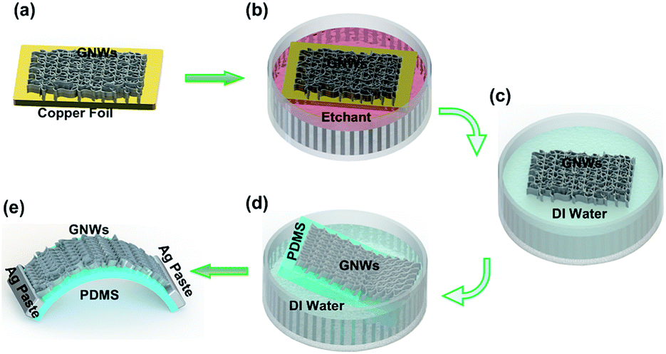 | ||
| Fig. 1 Schematic process for the fabrication of GNWs/PDMS temperature sensors. (a) Synthesizing GNWs on copper foils. (b) Dissolving copper foils in iron nitride solution. (c) Washing out the etchant residue by DI water. (d) Transferring GNWs onto the flexible PDMS film. (e) Brushing electrodes on the wearable sensor by Ag paste. | ||
Fabrication of GNWs/PDMS temperature sensors
Compared with the conventional transfer method, a PMMA (polymethylmethacrylate)-free transfer method was adopted to retain the vertical morphology of GNWs, which is important for high sensitivity temperature detection (Fig. 1b). After the complete dissolution of the underlying copper foils in 0.2 M aqueous Fe(NO3)3 solution overnight, the floating GNWs film was washed several times in deionized (DI) water to remove the remaining etchants (Fig. 1c), and then carefully transferred to the target substrate of a prepared PDMS film (500 μm thick). Afterwards, the GNWs/PDMS sample was dried in air or nitrogen gas and heated at 100 °C for 15 min to form a stable GNWs/PDMS temperature sensor (Fig. 1d). Finally, a simple two-terminal thermal resistor was achieved by brushing Ag paste on both sides of the GNW film to form the wearable temperature sensors (Fig. 1e). In this work, the distance between two silver electrodes was 20 mm and the width of GNWs film was 10 mm for every sample. The thickness of Ag electrodes should be large enough to guarantee good electrical contact.Characterization
Surface morphology of GNWs was analyzed by scanning electron microscopy (JEOL JSM-7800F), operating at 10 kV. Micro/nanostructure characterization is performed by HRTEM (FEI Tecnai G2 F20) operating at 200 kV. The carbon derivatives were verified by Raman spectroscopy measurements performed via confocal Raman microspectroscopy (Renishaw inVia Reflex) with a laser excitation wavelength of 532 nm. The response of GNWs/PDMS film to temperature was investigated by electrochemical workstation (CHI 760E, with a measurement accuracy ±20 pA) over a temperature range from 25 °C to 120 °C. In order to explore the essence of the thermal response, an atomic force microscopy (AFM) with a Thermal Applications Controller (Bruker, Dimension Edge AFM heater/cooler, with a high accuracy of 0.1 °C from −35 °C to 250 °C) was applied to observe the morphological change of GNWs films at different temperatures. A Nikon optical microscopy with video camera was adopted to investigate the in situ morphology evolution of the GNWs/PDMS film under different temperatures. In order to obtain a stable and reliable experimental data, we conducted our electrical characterization under a constant temperature and humidity environment (25 ± 1 °C, 50% ± 5%RH).Results and discussion
Fig. 2a shows the typical top-view SEM image of GNWs, which reveals that the entire surface is fully covered by continuous free-standing graphene nanosheets with typical size of 0.2–2 μm. The corresponding cross-sectional SEM image of GNWs is presented in Fig. 2b. It is clear that these graphene nanosheets are almost vertical on the substrate, forming a wall-like structure with a high aspect ratio. The height of GNWs evaluated from the cross-sectional SEM image was approximately 500 nm. Compared with the as-grown GNWs film on copper foil, this polymer-assisted transfer method retained the interlaced morphology of GNWs on PDMS film (Fig. S1†). The composition of a single nanosheet was further characterized by high-resolution TEM. From Fig. 2c, we can see that a nanosheet is composed of several graphene layers with spacing of about 0.35 nm. In addition, two low magnification TEM images show further evidence of an interlaced GNWs network (Fig. S2†). Raman spectroscopy was also employed to identify the quality of graphene nanosheets and the result is depicted in Fig. 2d, which shows a strong D band peak at 1348 cm−1 and a D′ band peak at 1615 cm−1, indicating that vast edges and defects exist in the graphene nanosheets.33 These graphene nanosheets edges are connected with each other forming a myriad of conductive channels, and hence provide a reliable and recoverable conductive network to adapt thermal expansion.26,27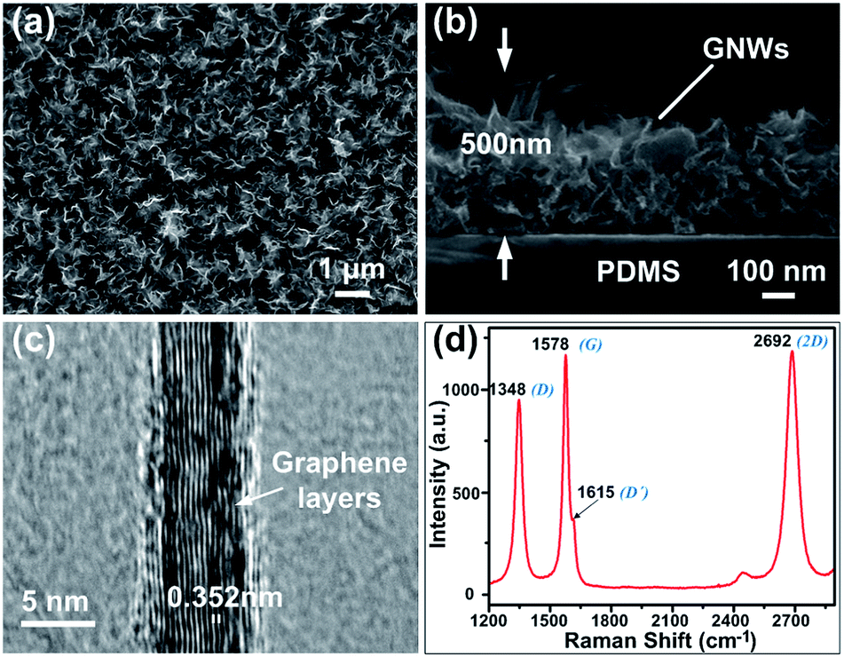 | ||
| Fig. 2 Characterization of GNWs on PDMS. (a) A typical SEM image of sheet-like GNWs film on PDMS. (b) The cross-section SEM image of GNWs on PDMS. (c) HRTEM image of GNWs shows graphene layers clearly. (d) Raman spectrum of GNWs on PDMS film. | ||
We transferred the as-grown GNWs film from copper foils to PDMS substrate, and fabricated a two terminal resistive temperature sensor (RTS), as schematically shown in Fig. 3a. It is worth noting that PDMS was chosen as a substrate because it is a flexible material with very high thermal coefficient of expansion (TCE), and therefore allow us to completely explore the stretchability of GNWs. The inset in Fig. 3a shows the flexibility of our prototype sensor. We investigated the response of the temperature sensor by measuring its resistance variation over a broad temperature range from room temperature (25 °C) to 120 °C. For each measurement, the temperature was first increased to the desired value, and then maintained as a constant for 10 minutes to assure a thermal equilibrium between the testing sample and the hotplate. A typical response curve is plotted on a logarithmic scale in Fig. 3b. In addition, the typical I–V characteristics were conducted and are shown in Fig. S3,† which shows an excellent ohmic contact between the GNWs film and the Ag electrodes. As can be seen from Fig. 3b, the resistance dramatically increases form 706.2 Ω at 25 °C to 98.04 kΩ at 120 °C, representing 138 fold variation. It is believed that such a high thermal response of the detector results from the excellent stretchability of GNWs and the large TCE of the PDMS substrate (the TCE of PDMS is 3.0 × 10⁻⁴ °C−1 from −55 to 150 °C (ref. 34 and 35)).
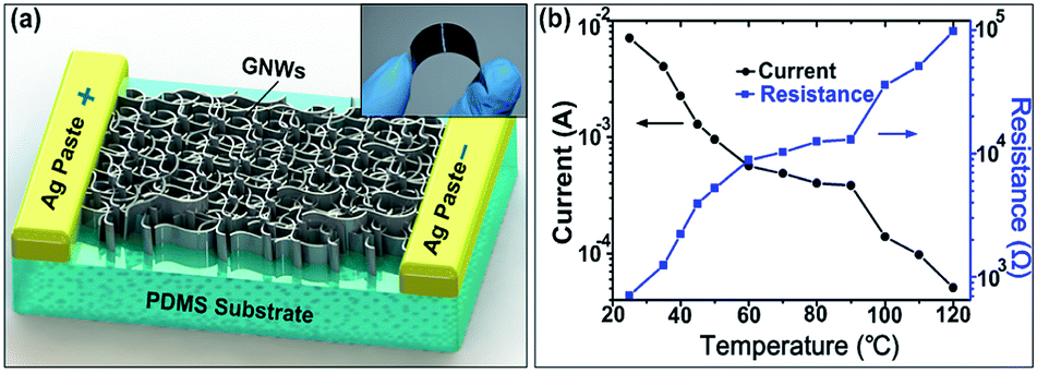 | ||
| Fig. 3 Thermal response of GNWs/PDMS sensor. (a) Schematic of flexible GNWs/PDMS temperature sensor with a simple structure. The inset shows the optical image of our fabricated flexible temperature sensor prototype. (b) Current and resistance versus temperature curves that range from room temperature (25 °C) to 120 °C by applying a constant voltage of 5 V at the two terminals of the sensor. | ||
To verify this idea, we employed optical microscopy to observe the morphology evolution of the GNWs film in situ as the temperature is varied by a thermal controller with a high accuracy of 0.1 °C. In Fig. 4a, the optical microscopy results are presented. As we increase the temperature from 25 °C to 120 °C, small cracks on the GNWs film are observed and the cracks become wider and denser at higher temperatures. Obviously, this phenomenon is caused by the expansion of the PDMS substrate. Interestingly, when we decrease the temperature, the cracks get smaller and eventually disappear and return to the original state, indicating that the morphology evolution process is reversible in our tested temperature range. More details are illustrated in the ESI Movie.† We then used AFM with the Thermal Applications Controller to monitor this process, cracks were observed at high temperatures, but then vanish at room temperature and return to the initial state (Fig. 4b). From the cross-section of the crack region (Fig. S4†), the above-mentioned changes are clear. The cracks become wider and deeper with increase in the temperature, for example, 0.8 μm width and 150 nm depth at 60 °C but 2.5 μm width and 500 nm depth at 120 °C. To view this process in more detail, a small area of 3 × 3 μm is scanned by AFM and the results are illustrated in Fig. 4c. It can be seen that the volume of an individual nanoflake gets larger and the density of the nanoflakes is smaller at higher temperature, signifying that the nanoflakes are also expanding and the distance between neighboring nanoflakes becomes larger (more details are show in Fig. S5†). Similarly, the opposite phenomenon appeared in the cooling process and the GNWs film would return to the initial interlaced network as observed by AFM. In addition, the cracks were becoming more obvious in terms of quantity and physical dimension from 90 °C, which is in accordance with the drastic change of curvature in Fig. 3b.
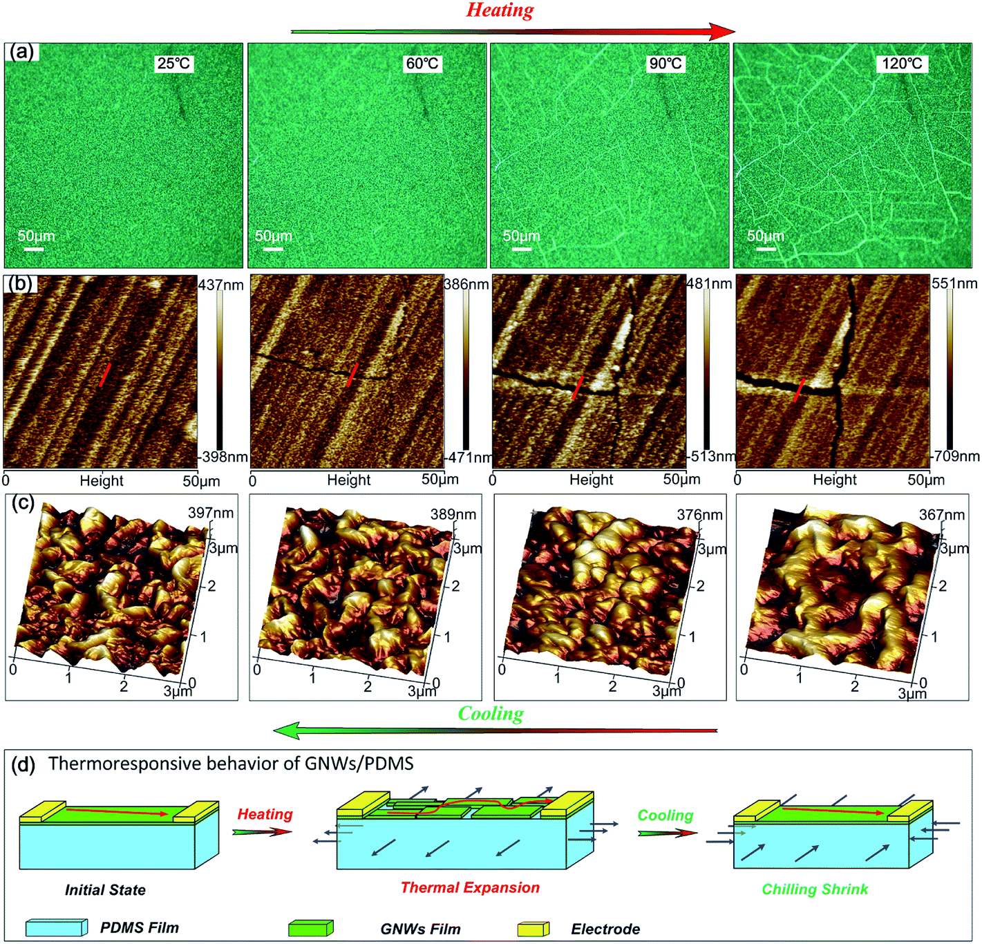 | ||
| Fig. 4 Surface morphological change of GNWs film under different temperatures from 25 to 120 °C. (a) The optical microscopy image of GNWs film on PDMS (600 × 600 μm). (b) The AFM image of cracks evolution on GNWs film (50 × 50 μm). (c) The AFM cross-section of the crack region (3 μm). (d) Schematic of thermal response/recovery of GNWs/PDMS film. | ||
Based on these observations, it becomes clear why our temperature sensor has such a high thermal response. During the temperature increase process, the interlaced GNWs network was stretched into a loosened conductive network by the radial expansion of the PDMS substrate, and cracks appeared due to the large TCE of PDMS. As a consequence, the compact graphene nano-sheets formed considerably longer conductive channels between the two electrodes, as shown in Fig. 4d, resulting in a significant increase in the resistance and extremely high thermal responsiveness. On the other hand, the conductive channels return to their original state after cooling. The high-density, mutual-crisscross graphene nano-flakes form a completely recoverable conductive channel during the process of thermal expansion and contraction of basal polymer (PDMS), resulting in excellent stability.
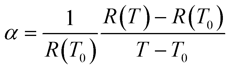
We measured the thermal response of our wearable temperature sensor in the range from 35 to 45 °C to investigate its ability to monitor human temperature with high accuracy. In Fig. 5a, the typical I–V characteristics are plotted, which shows that the current increases linearly with voltage, indicating that the conductive behaviour of the GNWs is ohmic contact. The obtained resistance from theses I–V curves are shown in the inset, it is evident that the resistance has a nearly linear dependence on temperature. The slope of the curve is related to the temperature coefficient of resistance (TCR) α, which is a key characteristic parameter of a temperature sensor and is defined as follows:
 | (1) |
 | ||
| Fig. 5 (a) I–V curves with a small interval of 1 °C range from 35 °C to 45 °C. The inset shows the current and resistance change rate curves as a function of temperature. (b) Characteristics over an extremely small temperature range, 35 to 36 °C, using a temperature interval of 0.1 °C. The inset illustrates the measurement process response to human body temperature. | ||
To further demonstrate the capability of our prototype temperature senor as a wearable device, we utilized it to measure the temperature of the human body. At first, the resistance over a temperature range of 35 to 36 °C with intervals of 0.1 °C (close to the normal body temperature) was measured to calibrate the sensor with a constant voltage of 5 V at the two terminals. The results are represented by blue squares in Fig. 5b. Then, as shown in the inset, the measured data was fitted by a linear curve with a slope of 108.6 Ω °C−1, R(T) = −5090.7 + 108.6T. Finally, we attached the sensor to the back of a hand (inset of Fig. 5b), and measured the resistance of the sensor. From the measured resistance of 1345.8 Ω, the body temperature was estimated to be 35.6 °C according to the fitted linear function indicating that the sensor is sensitive enough to monitor human body temperature.
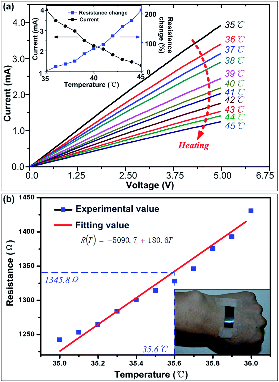
In addition to the temperature coefficient of resistance, the response and recovery time are also important parameters for a temperature sensor. We measured these parameters through the current variation of the sensor induced by its periodic contact and isolation with the hot plate when applied at a constant voltage of 5 V. The hot-zone of the hot plate was in full physical contact with the back side of the PDMS substrate to ensure fast thermal equilibrium between the sample and the hot-zone. In Fig. 6a, the graphs of current against time at temperatures of 60 °C, 90 °C and 120 °C are shown. Once the device touched the hot-zone from room temperature, the current dropped abruptly and saturated almost within one or two seconds. When the sensor was rapidly withdrawn from the hot-zone, the current increased exponentially back to the level at room temperature. Fig. 6c clearly shows that the response time is considerably shorter than the recovery time, and they can be calculated by fitting the curves using the following equation:37
|
I(t) = I0 + Aexp[−(t − B)/τ]
| (2) |
 | ||
| Fig. 6 Rapid response/recovery time of GNWs/PDMS temperature sensor. (a) High sensitivity measurement by rapid withdrawal from the hot-zone (60 °C, 90 °C, 120 °C) to room temperature. (b) Temperature sensing behavior under 60 °C for one period of time. The response/recovery time is calculated using eqn (1). (c) Response/recovery time curves under different temperatures. (d) The reliability of the GNWs/PDMS sensors over two months. | ||
In addition, we also evaluated the reliability of the temperature sensor. As shown in Fig. 6d, the current versus time curve is nearly unchanged after the sensor was exposed to ambient environment for 2 days, 2 weeks and 2 months, which suggests that the sensor, yet to be optimized, already shows excellent stability. The micro-nanoscale transformation of GNWs' morphology was investigated via optical microscopy and SEM images after 10 heating–cooling cycles as shown in Fig. S9.† It was found that there was no obvious change for both microscale and nanoscale morphology, and the stability of GNWs/PDMS temperature sensors was further verified.
Conclusion
In summary, a simple-structural temperature sensor based on GNWs/PDMS was developed by the plasma enhanced chemical vapor deposition technique and polymer-assisted transfer method. The TCR of the sensor reached 0.214 °C−1, which is three fold higher than that of conventional temperature sensors. Based on the optical and atomic force microscopy used to directly observe the morphology change of the GNWs/PDMS, it was demonstrated that such high response of the sensor stems from the excellent stretchability of GNWs and large expansion coefficient of PDMS. It was further shown that the sensor is sensitive enough to monitor the temperature of the human body, and can respond to temperature variation with relatively high speed. This type of temperature could find applications in the fields of flexible electronics, human health monitoring and human–machine interface.Acknowledgements
This work was supported by the National Natural Science Foundation of China (Grant no. NSFC 11404329, NSFC 11374359) and Natural Science Foundation of Chongqing (no. CSTC2012jjjq90001, CSTC 2012ggC50003, CSTC 2012ggC50001, CSTC2014jcyjjq50004), and the Project-sponsored by SRF for ROCS, SEM.Notes and references
- R. C. Webb, A. P. Bonifas, A. Behnaz, Y. Zhang, K. J. Yu, H. Cheng, M. Shi, Z. Bian, Z. Liu, Y.-S. Kim, W.-H. Yeo, J. S. Park, J. Song, Y. Li, Y. Huang, A. M. Gorbach and J. A. Rogers, Nat. Mater., 2013, 12, 938–944 CrossRef CAS PubMed.
- M. L. Hammock, A. Chortos, B. C. K. Tee, J. B. H. Tok and Z. A. Bao, Adv. Mater., 2013, 25, 5997–6037 CrossRef CAS PubMed.
- T. Nguyen Thanh, S. Jeon, D.-I. Kim, T. Tran Quang, M. Jang, B.-U. Hwang, K.-E. Byun, J. Bae, E. Lee, J. B. H. Tok, Z. Bao, N.-E. Lee and J.-J. Park, Adv. Mater., 2014, 26, 796–804 CrossRef PubMed.
- T. Someya, Y. Kato, T. Sekitani, S. Iba, Y. Noguchi, Y. Murase, H. Kawaguchi and T. Sakurai, Proc. Natl. Acad. Sci. U. S. A., 2005, 102, 12321–12325 CrossRef CAS PubMed.
- A. Chen, H.-Y. Chen and C. Chen, Sensors, 2014, 14, 15593–15609 CrossRef PubMed.
- C. D. S. Brites, P. P. Lima, N. J. O. Silva, A. Millan, V. S. Amaral, F. Palacio and L. D. Carlos, Nanoscale, 2012, 4, 4799–4829 RSC.
- J. Jeon, H.-B.-R. Lee and Z. Bao, Adv. Mater., 2013, 25, 850–855 CrossRef CAS PubMed.
- N. T. Tien, S. Jeon, D. I. Kim, T. Q. Trung, M. Jang, B. U. Hwang, K. E. Byun, J. Bae, E. Lee, J. B. H. Tok, Z. N. Bao, N. E. Lee and J. J. Park, Adv. Mater., 2014, 26, 796–804 CrossRef PubMed.
- M. Kaltenbrunner, T. Sekitani, J. Reeder, T. Yokota, K. Kuribara, T. Tokuhara, M. Drack, R. Schwoediauer, I. Graz, S. Bauer-Gogonea, S. Bauer and T. Someya, Nature, 2013, 499, 458–463 CrossRef CAS PubMed.
- J. J. Park and M. Taya, J. Electron. Packag., 2005, 127, 286–289 CrossRef CAS.
- T. H. Kim and S. J. Kim, J. Micromech. Microeng., 2006, 16, 2502–2508 CrossRef.
- Y. Moser and M. A. Gijs, J. Microelectromech. Syst., 2007, 16, 1349–1354 CrossRef CAS.
- J. Jeon, H. B. R. Lee and Z. Bao, Adv. Mater., 2013, 25, 850–855 CrossRef CAS PubMed.
- X. C. Ren, P. K. L. Chan, J. B. Lu, B. L. Huang and D. C. W. Leung, Adv. Mater., 2013, 25, 1291–1295 CrossRef CAS PubMed.
- J. T. W. Kuo, L. Yu and E. Meng, Micromachines, 2012, 3, 550–573 CrossRef PubMed.
- A. K. Geim and K. S. Novoselov, Nat. Mater., 2007, 6, 183–191 CrossRef CAS PubMed.
- A. K. Geim, Science, 2009, 324, 1530–1534 CrossRef CAS PubMed.
- M. Yoonessi, Y. Shi, D. A. Scheiman, M. Lebron-Colon, D. M. Tigelaar, R. A. Weiss and M. A. Meador, ACS Nano, 2012, 6, 7644–7655 CrossRef CAS PubMed.
- H.-B. Yao, J. Ge, C.-F. Wang, X. Wang, W. Hu, Z.-J. Zheng, Y. Ni and S.-H. Yu, Adv. Mater., 2013, 25, 6691 CrossRef.
- S. Bae, H. Kim, Y. Lee, X. F. Xu, J. S. Park, Y. Zheng, J. Balakrishnan, T. Lei, H. R. Kim, Y. I. Song, Y. J. Kim, K. S. Kim, B. Ozyilmaz, J. H. Ahn, B. H. Hong and S. Iijima, Nat. Nanotechnol., 2010, 5, 574–578 CrossRef CAS PubMed.
- H. Al-Mumen, F. Rao, L. Dong and W. Li, Micro Nano Lett., 2013, 8, 681–685 CAS.
- H. Al-Mumen, F. B. Rao, L. X. Dong and W. Li, Ieee, Design, Fabrication, and Characterization of Graphene Thermistor, Ieee, New York, 2013 Search PubMed.
- Y. M. Banadaki, K. M. Mohsin and A. Srivastava, Nanosensors, Biosensors, and Info-Tech Sensors and Systems, 2014, vol. 9060, p. 7 Search PubMed.
- T. Tran Quang, S. Ramasundaram, S. W. Hong and N.-E. Lee, Adv. Funct. Mater., 2014, 24, 3438–3445 CrossRef.
- T. Tran Quang, T. Nguyen Thanh, D. Kim, J. H. Jung, O. J. Yoon and N.-E. Lee, Adv. Mater., 2012, 24, 5254–5260 CrossRef PubMed.
- W. Takeuchi, M. Ura, M. Hiramatsu, Y. Tokuda, H. Kano and M. Hori, Appl. Phys. Lett., 2008, 92, 213103 CrossRef PubMed.
- Y. H. Wu, Nano Lett., 2002, 2, 355–359 CrossRef CAS.
- B. J. Yang, Y. H. Wu, B. Y. Zong and Z. X. Shen, Nano Lett., 2002, 2, 751–754 CrossRef CAS.
- H.-F. Yen, Y.-Y. Horng, M.-S. Hu, W.-H. Yang, J.-R. Wen, A. Ganguly, Y. Tai, K.-H. Chen and L.-C. Chen, Carbon, 2015, 82, 124–134 CrossRef CAS PubMed.
- M. Wang, X. Song, Q. Yang, H. Hua, S. Dai, C. Hu and D. Wei, J. Power Sources, 2014, 624–630 CrossRef PubMed.
- S. Evlashin, S. Svyakhovskiy, N. Suetin, A. Pilevsky, T. Murzina, N. Novikova, A. Stepanov, A. Egorov and A. Rakhimov, Carbon, 2014, 70, 111–118 CrossRef CAS PubMed.
- X. Song, J. Liu, L. Yu, J. Yang, L. Fang, H. Shi, C. Du and D. Wei, Mater. Lett., 2014, 137, 25–28 CrossRef CAS PubMed.
- M. Hiramatsu, K. Shiji, H. Amano and M. Hori, Appl. Phys. Lett., 2004, 84, 4708–4710 CrossRef CAS PubMed.
- N. Bowden, S. Brittain, A. G. Evans, J. W. Hutchinson and G. M. Whitesides, Nature, 1998, 393, 146–149 CrossRef CAS PubMed.
- A. Chiche, C. M. Stafford and J. T. Cabral, Soft Matter, 2008, 4, 2360–2364 RSC.
- A. Di Bartolomeo, M. Sarno, F. Giubileo, C. Altavilla, L. Iemmo, S. Piano, F. Bobba, M. Longobardi, A. Scarfato, D. Sannino, A. M. Cucolo and P. Ciambelli, J. Appl. Phys., 2009, 105, 064518 CrossRef PubMed.
- B. S. K. Sahoo and G. L. Sharma, arXiv preprint arXiv, 2012.
Footnotes |
| † Electronic supplementary information (ESI) available: Additional information can be found describing the SEM images of GNWs on copper foil and the low magnification TEM images of GNWs. Information regarding the AFM cross-section of crack region (red line in Fig. 4b, 6 μm) and GNWs film in Fig. 4c (3 μm) under different temperatures are also included. See DOI: 10.1039/c5ra00871a |
| ‡ The manuscript was written through the contributions of all the authors. All authors have given approval to the final version of the manuscript. |
| This journal is © The Royal Society of Chemistry 2015 |